��������� ��������� ��������� �������
��
����� � �� ����
����� ���
�� �
��
����
��
���� ���
����� �
���
SLVS296 − JUNE 2000
D Evaluation Module Available
features
(TPS60210EVM-167)
D Regulated 3.3-V Output Voltage From a
D
D
D
D
D
D
D
1.8-V to 3.6-V Input Voltage Range
UltraLow Operating Current in Snooze
Mode, Typical 2 µA
Less Than 5-mV(PP) Output Voltage Ripple
Achieved With Push-Pull Topology
Integrated Low-Battery and Power-Good
Detector
Switching Frequency Can Be Synchronized
to External Clock Signal
Extends Battery Usage With up to 90%
Efficiency and 35-µA Quiescent Current
Easy-To-Design, Low Cost, Low EMI Power
Supply Since No Inductors Are Used
Compact Converter Solution in UltraSmall
10-Pin MSOP With Only Four External
Capacitors Required
applications
D Replaces DC/DC Converters With Inductors
in Battery-Powered Applications Like:
− Two Battery Cells to 3.3-V Conversion
− MSP430 Ultralow-Power Microcontroller
and Other Battery Powered
Microprocessor Systems
− Glucose Meters and Other Medical
Instruments
− MP3 Portable Audio Players
− Backup-Battery Boost Converters
− Cordless Phones, PDAs
·
description
The TPS6021x step-up, regulated charge pumps generate a 3.3-V ±4% output voltage from a 1.8-V to 3.6-V
input voltage. These devices are typically powered by two alkaline, NiCd, or NiMH battery cells or by one primary
lithium MnO2 (or similar) coin cell and operate down to a minimum supply voltage of 1.6 V. Continuous output
current is a minimum of 100 mA for the TPS60210 and TPS60211, and 50 mA for the TPS60212 and TPS60213,
all from a 2-V input.
TPS60210
7
IN
OUT
5
R1
Ci
2.2 µ F
1
LBO
R2
4
C1
1 µF
3
9
ON/OFF
Co
2.2 µ F
R3
LBI
C1+
C2+
C1−
C2−
SNOOZE
GND
TPS60210
PEAK OUTPUT CURRENT
vs
INPUT VOLTAGE
OUTPUT
3.3 V
350
10
Low Battery
Warning
6
8
C2
1 µF
2
Figure 1. Typical Application Circuit With
Low-Battery Warning
IO − Output Current − mA
INPUT
1.6 V to 3.6 V
300
250
200
150
100
50
0
1.6
2.0
2.4
2.8
3.2
3.6
VI − Input Voltage − V
Please be aware that an important notice concerning availability, standard warranty,
and use in critical applications of
Texas Instruments semiconductor products and disclaimers thereto appears at the end of this data sheet.
Copyright 2000, Texas Instruments Incorporated
�
��
����� ���� �����!"#��� �$ %&��'�# "$ �� (&)*�%"#��� +"#'�
���+&%#$ %�����! #� $('%���%"#���$ ('� #,' #'�!$ �� �'-"$ ��$#�&!'�#$
$#"�+"�+ ."��"�#/� ���+&%#��� (��%'$$��0 +�'$ ��# �'%'$$"��*/ ��%*&+'
#'$#��0 �� "** ("�"!'#'�$�
POST OFFICE BOX 655303
• DALLAS, TEXAS 75265
1
���������� ��������� ��������� �������
��
����� � �� ����
����� ���
�� �
��
����
��
���� ���
����� �
���
SLVS296 − JUNE 2000
description (continued)
Three operating modes can be programmed using the SNOOZE pin. When SNOOZE is low, the device is put
into snooze mode. In snooze mode, the device operates with a typical quiescent current of 2 µA while the output
voltage is maintained at 3.3 V ±6%. This is lower than the self-discharge current of most batteries. Load current
in snooze mode is limited to 2 mA. When SNOOZE is high, the device is put into normal operating mode. During
normal operating mode, the device operates in the newly developed linskip mode where it switches seamlessly
from the power saving pulse-skip mode at light loads to the low-noise constant-frequency linear-regulation
mode once the output current exceeds the linskip current threshold of about 7 mA. In this mode, the device
operates from the internal oscillator. The device is synchronized to an external clock signal if SNOOZE is
clocked; thus switching harmonics can be controlled and minimized.
Only four external capacitors are needed to build a complete low-ripple dc/dc converter. The push-pull operating
mode of two single-ended charge pumps assures the low output voltage ripple as charge is continuously
transferred to the output. All the devices can start with full load current. The devices include a low-battery
detector that issues a warning if the battery voltage drops below a user-defined threshold voltage or a
power-good detector that goes active when the output voltage reaches about 90% of its nominal value. This
dc/dc converter requires no inductors; therefore, EMI of the system is reduced to a minimum, making it easier
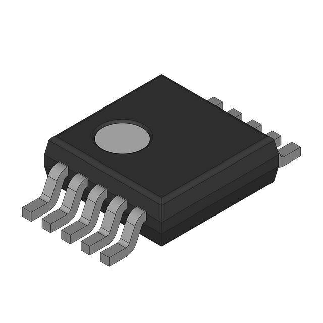
to use in designs. It is available in the small 10-pin MSOP package (DGS).
DGS PACKAGES
TPS60211
TPS60213
TPS60210
TPS60212
LBI
GND
C1−
C1+
OUT
1
10
2
9
3
8
4
7
5
6
GND
GND
C1−
C1+
OUT
LBO
SNOOZE
C2−
IN
C2+
1
10
2
9
3
8
4
7
5
6
PG
SNOOZE
C2−
IN
C2+
AVAILABLE OPTIONS
TA
−40°C to 85°C
PART NUMBER†
MARKING
DGS
PACKAGE
OUTPUT
CURRENT
(mA)
OUTPUT
VOLTAGE
(V)
TPS60210DGS
AFD
100
3.3
Low-battery detector
TPS60211DGS
AFE
100
3.3
Power-good detector
TPS60212DGS
AFF
50
3.3
Low-battery detector
TPS60213DGS
AFG
50
3.3
Power-good detector
DEVICE FEATURES
† The DGS package is available taped and reeled. Add R suffix to device type (e.g., TPS60210DGSR) to order
quantities of 3000 devices per reel.
2
POST OFFICE BOX 655303
• DALLAS, TEXAS 75265
���������� ��������� ��������� �������
��
����� � �� ����
����� ���
�� �
��
����
��
���� ���
����� �
���
SLVS296 − JUNE 2000
functional block diagrams
TPS60210 and TPS60212 with low-battery detector
Charge Pump 1
0°
IN
Oscillator
180°
C1+
C1
C1−
SNOOZE
Charge Pump 2
Control
Circuit
C2+
_
C2−
C2
+
VREF
Shutdown/
Start-Up
Control
+
−
OUT
_
_
+
LBI
+
+
−
0.8 x VIN
VREF
GND
+
−
LBO
TPS60211 and TPS60213 with power-good detector
Charge Pump 1
0°
Oscillator
180°
IN
C1+
C1
C1−
SNOOZE
Charge Pump 2
Control
Circuit
C2+
_
C2−
C2
+
VREF
Shutdown/
Start-Up
Control
+
−
OUT
_
_
+
+
+
−
0.8 x VIN
VREF
GND
POST OFFICE BOX 655303
+
−
PG
• DALLAS, TEXAS 75265
3
���������� ��������� ��������� �������
��
����� � �� ����
����� ���
�� �
��
����
��
���� ���
����� �
���
SLVS296 − JUNE 2000
Terminal Functions
TERMINAL
NAME
NO.
I/O
DESCRIPTION
C1+
4
Positive terminal of the flying capacitor C1
C1−
3
Negative terminal of the flying capacitor C1
C2+
6
Positive terminal of the flying capacitor C2
C2−
8
Negative terminal of the flying capacitor C2
GND
2
IN
7
I
Supply input. Bypass IN to GND with a capacitor of a minimum of 2.2 µF.
LBI/GND
1
I
Low-battery detector input for TPS60210 and TPS60212. A low-battery warning is generated at the LBO pin when
the voltage on LBI drops below the threshold of 1.18 V. Connect LBI to GND or VBAT if the low-battery detector
function is not used. For the devices TPS60211 and TPS60213, this pin is a ground (GND pin).
Ground
LBO/PG
10
O
OUT
5
O
Open-drain low-battery detector output for TPS60210 and TPS60212. This pin is pulled low if the voltage on LBI
drops below the threshold of 1.18 V. A pullup resistor should be connected between LBO and OUT or any other
logic supply rail that is lower than 3.6 V.
Open-drain power-good detector output for TPS60211 and TPS60213. As soon as the voltage on OUT reaches
about 90% of its nominal value, this pin goes active high. A pullup resistor should be connected between PG and
OUT or any other logic supply rail that is lower than 3.6 V.
Regulated 3.3-V power output. Bypass OUT to GND with the output filter capacitor Co.
Three operating modes can be programmed with the SNOOZE pin.
SNOOZE
9
I
− SNOOZE = Low programs the device in the snooze mode, enabling ultralow operating current while still
maintaining the output voltage to within 3.3 V ±6%.
− SNOOZE = High programs the device into normal operation mode where it runs from the internal oscillator.
− If an external clock signal is applied to the SNOOZE pin, the charge pump operates synchronized to the
frequency of the external clock signal.
detailed description
operating principle
The TPS6021x charge pumps provide a regulated 3.3-V output from a 1.8-V to 3.6-V input. They deliver a
minimum 100-mA load current while maintaining the output at 3.3 V ±4%. Designed specifically for space critical
battery-powered applications, the complete converter requires only four external capacitors. The device is using
the push-pull topology to achieve the lowest output voltage ripple. The converter is also optimized for a very
small board space. It makes use of small-sized capacitors, with the highest output current rating per output
capacitance.
The TPS6021x circuits consist of an oscillator, a voltage reference, an internal resistive feedback circuit, an error
amplifier, two charge-pump power stages with high-current MOSFET switches, a shutdown/start-up circuit, and
a control circuit (see functional block diagrams).
push-pull operating mode
The two single-ended charge-pump power stages operate in the push-pull operating mode (i.e., they operate
with a 180°C phase shift). Each single-ended charge pump transfers a charge into its flying capacitor (C1 or
C2) in one-half of the period. During the other half of the period (transfer phase), the flying capacitor is placed
in series with the input to transfer its charge to the load and output capacitor (Co). While one single-ended charge
pump is in the charge phase, the other one is in the transfer phase. This operation ensures that there is a
continuous flow of charge to the load, hence the output capacitor no longer needs to buffer the load current for
half of the switching cycle, avoiding the high, inherent output voltage ripple of conventional charge pumps.
In order to provide a regulated output voltage of 3.3 V, the TPS6021x devices operate either in
constant-frequency linear-regulation control mode or in pulse-skip mode. The mode is automatically selected
based on the output current. If the load current is low, the controller switches into the power-saving pulse-skip
mode to boost efficiency at low output power.
4
POST OFFICE BOX 655303
• DALLAS, TEXAS 75265
���������� ��������� ��������� �������
��
����� � �� ����
����� ���
�� �
��
����
��
���� ���
����� �
���
SLVS296 − JUNE 2000
detailed description (continued)
constant-frequency mode
When the output current is higher than the linskip current threshold, the charge pump runs continuously at the
switching frequency fOSC. The control circuit, fed from the error amplifier, controls the charge on C1 and C2 by
regulating the rDS(on) of the integrated MOSFET switches. When the output voltage decreases, the rDS(on)
decreases as well, resulting in a larger voltage across the flying capacitors C1 and C2. This regulation scheme
minimizes output ripple.
Since the device switches continuously, the output ripple contains well-defined frequency components, and the
circuit requires smaller external capacitors for a given output ripple. However, constant-frequency mode, due
to higher operating current, is less efficient at light loads. For this reason, the device switches seamlessly into
the pulse-skip mode when the output current drops below the linskip current threshold.
pulse-skip mode
The device enters the pulse-skip mode when the load current drops below the linskip current threshold of about
7 mA. In pulse-skip mode, the controller disables switching of the power stages when it detects an output voltage
higher than 3.3 V. It skips switching cycles until the output voltage drops below 3.3 V. Then the controller
reactivates the oscillator and switching of the power stages starts again. A 30-mV output voltage offset is
introduced in this mode.
The pulse-skip regulation mode minimizes operating current because it does not switch continuously and
deactivates all functions except the voltage reference and error amplifier when the output is higher than 3.3 V.
Even in pulse-skip mode the rDS(ON) of the MOSFETs is controlled. This way the energy per switching cycle that
is transferred by the charge pump from the input to the output is limited to the minimum that is necessary to
sustain a regulated output voltage, with the benefit that the output ripple is kept to a minimum. When switching
is disabled in pulse-skip mode, the load is isolated from the input.
start up, snooze mode, short circuit protection
During start-up (i.e., when voltage is applied to the supply pin IN) the input is connected to the output until the
output voltage reaches 0.8 x VI. When the start-up comparator detects this limit, the actual charge pump output
stages are activated to boost the voltage higher than the input voltage. This precharging of the output current
with a limited current ensures a short start-up time and avoids high inrush currents into an empty output
capacitor.
Driving SNOOZE low, programs the device into the snooze mode. In this mode, the converter will still maintain
the output voltage at 3.3 V ±6%. The operating current in snooze mode, is however, drastically reduced to a
typical value of 2 µA, while the output current is limited to a maximum of 2 mA. If the load current increases above
2 mA, the controller recognizes a further drop of the output voltage and the device enters the start-up mode to
bring the voltage up to its nominal value again. However, it does not switch into the normal operating mode. The
device limits short circuit currents to typically 60 mA.
synchronization to an external clock signal
The operating frequency of the charge pump is limited to 400 kHz in order to avoid troublesome interference
problems in the sensitive 455-kHz IF band. The device can either run from the integrated oscillator, or an
external clock signal can be used to drive the charge pump. The maximum frequency of the external clock signal
is 800 kHz. The switching frequency used internally to drive the charge pump power stages is half of the external
clock frequency. The external clock signal is applied to the SNOOZE-pin. The device will switch into the snooze
mode if the signal on SNOOZE is held low for more than 10 µs.
When the load current drops below the linskip current threshold, the device enters the pulse-skip mode but stays
synchronized to the external clock signal.
POST OFFICE BOX 655303
• DALLAS, TEXAS 75265
5
���������� ��������� ��������� �������
��
����� � �� ����
����� ���
�� �
��
����
��
���� ���
����� �
���
SLVS296 − JUNE 2000
detailed description (continued)
low-battery detector (TPS60210 and TPS60212)
The low-battery comparator trips at 1.18 V ±5% when the voltage on pin LBI ramps down. The voltage V(TRIP)
at which the low-battery warning is issued can be adjusted with a resistive divider as shown in Figure 2. The
sum of resistors R1 and R2 is recommended to be in the 100-kΩ to 1-MΩ range.
LBO is an open drain output. An external pullup resistor to OUT, or any other voltage rail in the appropriate range,
in the 100-kΩ to 1-MΩ range is recommended. During start-up, the LBO output signal is invalid for the first
500 µs. LBO is high impedance when the device is programmed into snooze mode.
If the low battery function is not used, connect LBI to ground and leave LBO unconnected. When the device is
programmed into snooze mode (SNOOZE = LOW), the low-battery detector is disabled.
VO
IN
VBAT
R3
R1
LBO
_
+
VREF
ǒ
Ǔ
V (TRIP) + 1.18 V 1 ) R1
R2
LBI
R2
+
−
Figure 2. Programming of the Low-Battery Comparator Trip Voltage
A 100-nF ceramic capacitor should be connected in parallel to R2 if large line transients are expected. These
voltage drops may inadvertently trigger the low-battery comparator and produce a wrong low-battery warning
signal at the LBO pin.
Formulas to calculate the resistive divider for low-battery detection, with VLBI = 1.13 V to 1.23 V and the sum
of resistors R1 and R2 equal 1 MΩ:
V
LBI
(1)
Bat
R1 + 1 MW * R2
(2)
R2 + 1 MW
V
Formulas to calculate the minimum and maximum battery voltage:
R1
Bat(min)
+V
Bat(max)
+V
V
LBI(min)
(min)
R2
R1
V
6
LBI(max)
) R2
(max)
(3)
(max)
(max)
R2
) R2
(min)
(4)
(min)
POST OFFICE BOX 655303
• DALLAS, TEXAS 75265
���������� ��������� ��������� �������
��
����� � �� ����
����� ���
�� �
��
����
��
���� ���
����� �
���
SLVS296 − JUNE 2000
detailed description (continued)
Table 1. Recommended Values for the Resistive Divider From the E96 Series (±1%)
VIN/V
1.6
R1/kΩ
R2/kΩ
750
VTRIP(MIN)/V
1.524
VTRIP(MAX)/V
1.677
267
1.7
301
1.8
340
681
1.620
1.785
649
1.710
1.887
1.9
2.0
374
619
1.799
1.988
402
576
1.903
2.106
power-good detector (TPS60211 and TPS60213)
The power-good output is an open-drain output that pulls low when the output is out of regulation. When the
output rises above 91% of its nominal voltage, the power-good output is released. When the device is
programmed into snooze mode (SNOOZE = LOW), the power-good detector is disabled and PG is high
impedance. In normal operation, an external pullup resistor must be connected between PG and OUT, or any
other voltage rail in the appropriate range. The pullup resistor should be in the 100-kΩ to 1-MΩ range. If the PG
output is not used, it should remain unconnected.
absolute maximum ratings over operating free-air temperature range (unless otherwise noted)†
Voltage range:
IN, OUT, SNOOZE, LBI, LBO, PG to GND . . . . . . . . . . . . . . . . . . . . . . . . . . . . −0.3 V to 3.6 V
C1+, C2+ to GND . . . . . . . . . . . . . . . . . . . . . . . . . . . . . . . . . . . . . . . . . . −0.3 V to (VO + 0.3 V)
C1−, C2− to GND . . . . . . . . . . . . . . . . . . . . . . . . . . . . . . . . . . . . . . . . . . . . −0.3 V to (VI + 0.3 V)
Continuous total power dissipation . . . . . . . . . . . . . . . . . . . . . . . . . . . . . . . . . . . . . . See Dissipation Rating Table
Continuous output current: TPS60210, TPS60211 . . . . . . . . . . . . . . . . . . . . . . . . . . . . . . . . . . . . . . . . . . 150 mA
TPS60212, TPS60213 . . . . . . . . . . . . . . . . . . . . . . . . . . . . . . . . . . . . . . . . . . . 75 mA
Storage temperature range, Tstg . . . . . . . . . . . . . . . . . . . . . . . . . . . . . . . . . . . . . . . . . . . . . . . . . . . . −55°C to 150°C
Maximum junction temperature, TJ . . . . . . . . . . . . . . . . . . . . . . . . . . . . . . . . . . . . . . . . . . . . . . . . . . . . . . . . . 150°C
† Stresses beyond those listed under “absolute maximum ratings” may cause permanent damage to the device. These are stress ratings only, and
functional operation of the device at these or any other conditions beyond those indicated under “recommended operating conditions” is not
implied. Exposure to absolute-maximum-rated conditions for extended periods may affect device reliability.
DISSIPATION RATING TABLE 1 FREE-AIR TEMPERATURE
PACKAGE
TA ≤ 25°C
POWER RATING
DGS
424 mW
DERATING FACTOR
ABOVE TA = 25°C
3.4 mW/_C
TA = 70°C
POWER RATING
TA = 85°C
POWER RATING
178 mW
136 mW
The thermal resistance junction to ambient of the DGS package is RTH−JA = 294°C/W.
recommended operating conditions
MIN
Input voltage range, VI
NOM
1.6
Input capacitor, Ci
Flying capacitors, C1, C2
Output capacitor, Co
MAX
3.6
−40
POST OFFICE BOX 655303
• DALLAS, TEXAS 75265
V
2.2
µF
1
µF
µF
2.2
Operating junction temperature, TJ
UNIT
125
°C
7
���������� ��������� ��������� �������
��
����� � �� ����
����� ���
�� �
��
����
��
���� ���
����� �
���
SLVS296 − JUNE 2000
electrical characteristics at Ci= 2.2 µF, C1 = C2 = 1 µF, Co = 2.2 µF, TA = −40°C to 85°C, VI = 2.4 V,
SNOOZE = VI (unless otherwise noted)
PARAMETER
IO(MAX)
TEST CONDITIONS
Maximum continuous output current
Output voltage
VO
Output voltage in snooze mode
VPP
I(Q)
f(OSC)
f(SYNC)
Output voltage ripple
Quiescent current (no-load input current)
TYP
MAX
UNIT
100
mA
TPS60212 and TPS60213, VI = 2 V
50
mA
1.6 V < VI < 1.8 V, 0 < IO < 0.25 × IO(MAX)
3
1.8 V < VI < 2 V,
0 < IO < 0.5 × IO(MAX)
3.17
3.3
3.43
V
2 V < VI < 3.3 V,
0 < IO < IO(MAX)
3.17
3.3
3.43
V
3.3 V < VI < 3.6 V,
0 < IO < IO(MAX)
3.17
3.3
3.47
V
SNOOZE = GND,
IO < 2 mA
IO = IO(MAX)
1.8 V < VI < 3.6 V,
3.1
3.3
3.47
V
V
5
IO = 0 mA, VI = 1.8 V to 3.6 V
SNOOZE = GND, IO = 0 mA
35
70
mVPP
µA
2
5
µA
200
300
400
kHz
External clock signal frequency
400
600
800
kHz
External clock signal duty cycle
30%
Quiescent current in snooze mode
Internal switching frequency
VIL
VIH
SNOOZE input low voltage
SNOOZE input high voltage
VI = 1.6 V to 3.6 V
VI = 1.6 V to 3.6 V
Ilkg
SNOOZE input leakage current
SNOOZE = GND or VI
LinSkip current threshold
VI = 2 V to 3 V
VI = 2.4 V,
TC = 25°C
VI = 2.4 V,
TC = 25°C
2 V < VI < 3.3 V,
TA = 25°C
Output load regulation
Output line regulation
I(SC)
MIN
TPS60210 and TPS60211, VI = 2 V
Short circuit current
70%
0.3 × VI
V
0.1
µA
0.7 × VI
V
0.01
7
1 mA < IO < IO(MAX),
0.015
10 mA < IO < IO(MAX),
0.008
%/mA
IO = 0.5 x IO(MAX),
VI = 2.4 V,
mA
0.28
%V
60
mA
VO = 0 V
electrical characteristics for low-battery comparator of devices TPS60210 and TPS60212 at
TA = −40°C to 85°C, VI = 2.4 V and SNOOZE = VI (unless otherwise noted)
PARAMETER
V(LBI)
TEST CONDITIONS
LBI trip voltage
VI = 1.6 V to 2.2 V,
Tc = 0°C to 70°C
For rising voltage at LBI
LBI trip voltage hysteresis
II(LBI)
VO(LBO)
MIN
LBI input current
TYP
1.13
1.18
MAX
1.23
10
V(LBI) = 1.3 V
V(LBI) = 0 V,
20
LBO output voltage low
I(LBO) = 1 mA
Ilkg(LBO) LBO leakage current
V(LBI) = 1.3 V,
V(LBO) = 3.3 V
NOTE: During start-up of the converter the LBO output signal is invalid for the first 500 µs.
0.01
UNIT
V
mV
100
nA
0.4
V
0.1
µA
electrical characteristics for power-good comparator of devices TPS60211 and TPS60213 at
TA = −40°C to 85°C, VI = 2.4 V and SNOOZE = VI (unless otherwise noted)
PARAMETER
V(PG)
Vhys(PG)
Power-good trip voltage
VO(PG)
Ilkg(PG)
Power-good output voltage low
TEST CONDITIONS
Power-good trip voltage hysteresis
Tc = 0°C to 70°C
VO decreasing, Tc = 0°C to 70°C
I(PG) = 1 mA
V(PG) = 3.3 V
NOTE: During start-up of the converter the PG output signal is invalid for the first 500 µs.
8
Power-good leakage current
VO = 0 V,
VO = 3.3 V,
POST OFFICE BOX 655303
• DALLAS, TEXAS 75265
MIN
TYP
MAX
UNIT
0.87 × VO
0.91 × VO
0.95 × VO
V
1%
0.01
0.4
V
0.1
µA
���������� ��������� ��������� �������
��
����� � �� ����
����� ���
�� �
��
����
��
���� ���
����� �
���
SLVS296 − JUNE 2000
TYPICAL CHARACTERISTICS
Table of Graphs
FIGURES
vs Output current (TPS60210 and TPS60212)
η
Efficiency
IO
Output current
VO
Output voltage
IQ
Quiescent supply current
VO
Output voltage
VO
Output voltage ripple
3, 4
vs Input voltage
5
vs Input voltage
6
vs Output current (TPS60210 and TPS60212)
7, 8
vs Input voltage (TPS60210 and TPS60212)
9, 10
vs Input voltage
11
vs Output current in snooze mode
12
vs Time (Exit from snooze mode)
13
vs Time
14, 15, 16
vs Time in snooze mode
17, 18
Load transient response
19
Line transient response
20
TPS60210
TPS60212
EFFICIENCY
vs
OUTPUT CURRENT
EFFICIENCY
vs
OUTPUT CURRENT
100
100
90
90
80
80
70
70
Efficiency − %
Efficiency − %
NOTE: All typical characteristics were measured using the typical application circuit of Figure 21 (unless otherwise noted).
60
VI = 1.8 V
50
VI = 2.4 V
40
VI = 2.7 V
30
60
50
20
10
10
1
VI = 2.4 V
30
20
0
0.1
VI = 1.8 V
40
10
100
1000
0
0.1
IO − Output Current − mA
VI = 2.7 V
1
10
100
IO − Output Current − mA
Figure 3
Figure 4
POST OFFICE BOX 655303
• DALLAS, TEXAS 75265
9
���������� ��������� ��������� �������
��
����� � �� ����
����� ���
�� �
��
����
��
���� ���
����� �
���
SLVS296 − JUNE 2000
TYPICAL CHARACTERISTICS
TPS60210
PEAK OUTPUT CURRENT
vs
INPUT VOLTAGE
TPS60210
EFFICIENCY
vs
INPUT VOLTAGE
100
350
90
300
IO − Output Current − mA
80
Efficiency − %
70
60
50
IO = 50 mA
40
30
250
200
150
100
20
50
10
0
1.6
2.0
2.4
2.8
VI − Input Voltage − V
3.2
0
1.6
3.6
2.0
2.4
2.8
Figure 5
TPS60210
TPS60212
OUTPUT VOLTAGE
vs
OUTPUT CURRENT
OUTPUT VOLTAGE
vs
OUTPUT CURRENT
3.35
VI = 2.7 V
VI = 3.6 V
3.30
3.4
VO − Output Voltage − V
VI = 3.6 V
VO − Output Voltage − V
3.6
Figure 6
3.5
3.3
3.2
VI = 1.8 V
VI = 2.7 V
3.1
VI = 2.4 V
3.0
3.25
VI = 1.8 V
VI = 2.4 V
3.20
3.15
3.10
3.05
3
2.9
1
10
100
1000
1
10
IO − Output Current − mA
IO − Output Current − mA
Figure 8
Figure 7
10
3.2
VI − Input Voltage − V
POST OFFICE BOX 655303
• DALLAS, TEXAS 75265
100
���������� ��������� ��������� �������
��
����� � �� ����
����� ���
�� �
��
����
��
���� ���
����� �
���
SLVS296 − JUNE 2000
TYPICAL CHARACTERISTICS
TPS60210
TPS60212
OUTPUT VOLTAGE
vs
INPUT VOLTAGE
OUTPUT VOLTAGE
vs
INPUT VOLTAGE
3.4
3.35
3.30
1 mA
3.2
3.1
VO − Output Voltage − V
VO − Output Voltage − V
3.3
50 mA
100 mA
3.0
2.9
2.8
2.7
1.6
1 mA
3.25
3.20
25 mA
50 mA
3.15
3.10
3.05
2.0
2.4
3.2
2.8
3.00
1.6
3.6
VI − Input Voltage − V
2.0
QUIESCENT SUPPLY CURRENT
vs
INPUT VOLTAGE
70
IO = 0 mA
SNOOZE = VI
VI = 2.4 V
SNOOZE = GND
60
I − Quiescent Current − µ A
Q
I − Quiescent Current − µ A
Q
3.6
QUIESCENT SUPPLY CURRENT
vs
OUTPUT CURRENT IN SNOOZE MODE
40
36
3.2
Figure 10
Figure 9
38
2.4
2.8
VI − Input Voltage − V
34
32
30
28
26
50
40
30
20
24
10
22
20
1.6 1.8 2.0 2.2 2.4 2.6 2.8 3.0 3.2 3.4 3.6
0
0
0.2 0.4
0.6 0.8
1
1.2 1.4
1.6
1.8
2
IO − Output Current − mA
VI − Input Voltage − V
Figure 11
Figure 12
POST OFFICE BOX 655303
• DALLAS, TEXAS 75265
11
���������� ��������� ��������� �������
��
����� � �� ����
����� ���
�� �
��
����
��
���� ���
����� �
���
SLVS296 − JUNE 2000
TYPICAL CHARACTERISTICS
TPS60210
TPS60210
OUTPUT VOLTAGE RIPPLE
vs
TIME
3.6
3.38
3.5
3.36
3.4
3.34
VO− Output Voltage − V
VO − Output Voltage − V
OUTPUT VOLTAGE
vs
TIME
3.3
SNOOZE
3.2
VI = 2.4 V
IO = 1 mA
3.32
3.30
3.28
3.26
High
3.24
Low
3.22
0
50 100 150 200 250 300 350 400 450 500
t − Time − ms
0
5
10
15
40
TPS60210
TPS60210
OUTPUT VOLTAGE RIPPLE
vs
TIME
OUTPUT VOLTAGE RIPPLE
vs
TIME
45
50
9
10
3.38
3.38
VI = 2.4 V
IO = 10 mA
3.36
VI = 2.4 V
IO = 100 mA
3.36
3.34
VO− Output Voltage − V
3.34
VO− Output Voltage − V
35
Figure 14
Figure 13
3.32
3.30
3.28
3.26
3.32
3.30
3.28
3.26
3.24
3.24
3.22
3.22
0
1
2
3
4
5
6
t − Time − µs
7
8
9
10
0
1
Figure 15
12
20 25 30
t − Time − µs
2
3
4
5
6
t − Time − µs
Figure 16
POST OFFICE BOX 655303
• DALLAS, TEXAS 75265
7
8
���������� ��������� ��������� �������
��
����� � �� ����
����� ���
�� �
��
����
��
���� ���
����� �
���
SLVS296 − JUNE 2000
TYPICAL CHARACTERISTICS
TPS60210
TPS60210
OUTPUT VOLTAGE RIPPLE IN SNOOZE MODE
vs
TIME
OUTPUT VOLTAGE RIPPLE IN SNOOZE MODE
vs
TIME
3.7
3.7
VI = 2.4 V
IO = 1 mA
CO = 10 µF (Tantalum)
SNOOZE = Low
3.5
VO − Output Voltage − V
VO − Output Voltage − V
3.6
VI = 2.4 V
IO = 1 mA
CO = 2.2 µF (Ceramic)
SNOOZE = Low
3.6
3.4
3.3
3.2
3.5
3.4
3.3
3.2
3.1
3.1
3
3
2.9
2.9
0
0
100 200 300 400 500 600 700 800 900 1000
100 200 300 400 500 600 700 800 900 1000
t − Time − µs
t − Time − µs
Figure 18
TPS60210
LINE TRANSIENT RESPONSE
VI = 2.4 V
3.30
3.28
3.26
VO − Output Voltage − V
TPS60210
LOAD TRANSIENT RESPONSE
3.24
IO = 50 mA
3.32
3.30
3.28
VI − Input Voltage − V
I O− Output Current − mA
VO − Output Voltage − V
Figure 17
100 mA
10 mA
0
50
100 150 200 250 300 350 400 450 500
3.26
2.8 V
2.2 V
0
1
t − Time − µs
2
3
4
5
6
7
8
9
10
t − Time − ms
Figure 19
Figure 20
POST OFFICE BOX 655303
• DALLAS, TEXAS 75265
13
���������� ��������� ��������� �������
��
����� � �� ����
����� ���
�� �
��
����
��
���� ���
����� �
���
SLVS296 − JUNE 2000
APPLICATION INFORMATION
capacitor selection
The TPS6021x devices require only four external capacitors to achieve a very low output voltage ripple. The
capacitor values are closely linked to the required output current. Low ESR (< 0.1-Ω) capacitors should be used
at the input and output of the charge pump. In general, the transfer capacitors (C1 and C2) will be the smallest.
A 1-µF value is recommended if full load current performance is needed. With smaller capacitor values, the
maximum possible load current is reduced and the linskip threshold is lowered.
The input capacitor improves system efficiency by reducing the input impedance. It also stabilizes the input
current of the power source. The input capacitor should be chosen according to the power supply used, the
distance from the power source to the converter IC. CI is recommended to be about two to four times as large
as the flying capacitors C1 and C2.
The minimum required capacitance is 2.2 µF. Larger values will improve the load transient performance and
will reduce the maximum output ripple voltage. The larger the output capacitor, the better the output voltage
accuracy, and the more output current can be drawn from the converter when programmed into snooze mode.
Only ceramic capacitors are recommended for input, output and flying capacitors. Depending on the material
used to manufacture them, ceramic capacitors might lose their capacitance over temperature and voltage.
Ceramic capacitors of type X7R or X5R material will keep their capacitance over temperature and voltage,
whereas Z5U- or Y5V-type capacitors will decrease in capacitance. Table 1 lists recommended capacitor
values.
14
POST OFFICE BOX 655303
• DALLAS, TEXAS 75265
���������� ��������� ��������� �������
��
����� � �� ����
����� ���
�� �
��
����
��
���� ���
����� �
���
SLVS296 − JUNE 2000
APPLICATION INFORMATION
Table 2. Recommended Capacitor Values (Ceramic X5R and X7R)
LOAD CURRENT,
ILOAD
(mA)
FLYING
CAPACITORS,
C1/C2
(µF)
INPUT
CAPACITOR,
CIN
(µF)
OUTPUT
CAPACITOR,
COUT
(µF)
OUTPUT VOLTAGE
RIPPLE IN LINEAR MODE,
VP-P
(mV)
OUTPUT VOLTAGE
RIPPLE IN SKIP MODE,
VP-P
(mV)
0−100
1
2.2
2.2
3
20
0−100
1
4.7
4.7
3
10
0−100
1
2.2
10
3
7
0−100
2.2
4.7
4.7
3
10
0−50
0.47
2.2
2.2
3
20
0−25
0.22
2.2
2.2
5
15
0−10
0.1
2.2
2.2
5
15
Table 3. Recommended Capacitor Types
MANUFACTURER
Taiyo Yuden
AVX
PART NUMBER
SIZE
CAPACITANCE
TYPE
UMK212BJ104MG
0805
0.1 µF
Ceramic
EMK212BJ224MG
0805
0.22 µF
Ceramic
EMK212BJ474MG
0805
0.47 µF
Ceramic
LMK212BJ105KG
0805
1 µF
Ceramic
LMK212BJ225MG
0805
2.2 µF
Ceramic
EMK316BJ225KL
1206
2.2 µF
Ceramic
LMK316BJ475KL
1206
4.7 µF
Ceramic
JMK316BJ106ML
1206
10 µF
Ceramic
0805ZC105KAT2A
0805
1 µF
Ceramic
1206ZC225KAT2A
1206
2.2 µF
Ceramic
Table 4. Recommended Capacitor Manufacturers
MANUFACTURER
CAPACITOR TYPE
INTERNET SITE
Taiyo Yuden
X7R/X5R ceramic
http://www.t−yuden.com/
AVX
X7R/X5R ceramic
http://www.avxcorp.com/
POST OFFICE BOX 655303
• DALLAS, TEXAS 75265
15
���������� ��������� ��������� �������
��
����� � �� ����
����� ���
�� �
��
����
��
���� ���
����� �
���
SLVS296 − JUNE 2000
APPLICATION INFORMATION
typical operating circuit TPS60210
INPUT
1.8 V to 3.6 V
7
R1
Ci
2.2 µF
1
R3
LBI
LBO
R2
4
OUTPUT
3.3 V, 100 mA
TPS60210
5
IN
OUT
C1+
C2+
Co
2.2 µF
10
Low Battery
Warning
6
C1
1 µF
3
8
C1−
C2−
9
SNOOZE
GND
ON/OFF
2
C2
1 µF
Figure 21. Typical Operating Circuit TPS60210 With Low-Battery Comparator
INPUT
1.6 V to 3.6 V
Ci
2.2 µF
7
R1
1
ON/OFF
R3
LBI
LBO
R2
4
C1
0.47 µF
3
9
OUTPUT
3.3 V, 50 mA
TPS60212
5
IN
OUT
C1+
C2+
C1−
C2−
Co
2.2 µF
10
Low Battery
Warning
6
8
C2
0.47 µF
SNOOZE
GND
2
Figure 22. Typical Operating Circuit TPS60212 With Low-Battery Comparator
The current losses through the resistive divider used to set the low-battery threshold can be avoided if an
additional MOSFET (like BSS138) is used in series to the resistors. This switch is controlled using the SNOOZE
signal. When the SNOOZE-signal is taken high, the device is programmed into normal operating mode, the
switch will turn on and the resistive divider draws current to set the LBI threshold voltage. When SNOOZE is
taken low, the device is programmed into snooze mode during which the low-battery comparator is disabled.
In addition, the resistive divider R1/R2 is disconnected from GND and therefore draws no current from the
battery. A typical schematic for this circuit is shown in Figure 22.
16
POST OFFICE BOX 655303
• DALLAS, TEXAS 75265
���������� ��������� ��������� �������
��
����� � �� ����
����� ���
�� �
��
����
��
���� ���
����� �
���
SLVS296 − JUNE 2000
APPLICATION INFORMATION
typical operating circuit TPS60211
INPUT
1.8 V to 3.6 V
7
OUTPUT
3.3 V, 100 mA
TPS60211
5
IN
OUT
Ci
2.2 µF
R1
PG
4
C1+
C2+
C1
1 µF
Co
2.2 µF
10
6
3
8
C1−
C2−
9
SNOOZE
GND
ON/OFF
1,2
Power-Good Signal
C2
1 µF
Figure 23. Typical Operating Circuit TPS60211 With Power-Good Comparator
power dissipation
The power dissipated in the TPS6021x devices depends mainly on input voltage (VI) and output current (IO)
and is approximated by:
P
(DISS)
+ I
O
ǒ
Ǔ
x 2xV * V
for I
tt I
I
O
(Q)
O
(5)
By observing equation 5, it can be seen that the power dissipation is worse with a higher input voltage and a
higher output current. For an input voltage of 3.6 V and an output current of 100 mA, the calculated power
dissipation (P(DISS)) is 390 mW. This is also the point where the charge pump operates with its lowest efficiency.
With the recommended maximum junction temperature of 125°C and an assumed maximum ambient operating
temperature of 85°C, the maximum allowed thermal resistance junction to ambient of the system can be
calculated.
R QJA(max) +
T J(MAX) * T A
P DISS(max)
+ 125°C * 85°C + 102°CńW
390 mW
(6)
PDISS must be less than that allowed by the package rating. The thermal resistance junction to ambient of the
used 10-pin MSOP is 294°C/W for an unsoldered package. The thermal resistance junction to ambient with the
IC soldered to a printed circuit using a board layout as described in the application information section, the RΘJA
is typically 200°C/W, which is higher than the maximum value calculated previously. However, in a battery
powered application, both the VI and the ambient temperature (TA) will typically be lower than the worst case
ratings used in equation 6, and PDISS should not be a problem in most applications.
layout and board space
Careful board layout is necessary due to the high transient currents and switching frequency of the converter.
All capacitors should be placed in close proximity to the device. A PCB layout proposal for a one-layer board
is given in Figure 24.
An evaluation module for the TPS60210 is available and can be ordered under product code
TPS60210EVM−167. The EVM uses the layout shown in Figure 26. The EVM has the form factor of a 14-pin
dual in-line package and can be mounted accordingly on a socket. All components, including the pins, are
shown in Figure 24. The actual size of the EVM is 17,9 mm x 10,2 mm = 182,6 mm2.
POST OFFICE BOX 655303
• DALLAS, TEXAS 75265
17
���������� ��������� ��������� �������
��
����� � �� ����
����� ���
�� �
��
����
��
���� ���
����� �
���
SLVS296 − JUNE 2000
APPLICATION INFORMATION
layout and board space (continued)
C1
R3
R2
IC1
C5
R1
C4
17,9 mm
10,2 mm
C3
R4
C2
Figure 24. Recommended Component Placement and Board Layout
Table 5. Component Identification
IC1
C1, C2
TPS60210
Flying capacitors
C3
Input capacitor
C4
Output capacitor
C5
Stabilization capacitor for LBI
R1, R2
Resistive divider for LBI
R3
Pullup resistor for LBO
R4
Pullup resistor for EN
Capacitor C5 should be included if large line transients are expected. This capacitor suppresses toggling of the
LBO due to these line changes.
18
POST OFFICE BOX 655303
• DALLAS, TEXAS 75265
���������� ��������� ��������� �������
��
����� � �� ����
����� ���
�� �
��
����
��
���� ���
����� �
���
SLVS296 − JUNE 2000
APPLICATION INFORMATION
device family products
Other charge pump dc-dc converters from Texas Instruments are:
Table 6. Product Identification
PART NUMBER
LITERATURE
NUMBER
DESCRIPTION
TPS60100
SLVS213
2-cell to regulated 3.3-V, 200-mA low-noise charge pump
TPS60101
SLVS214
2-cell to regulated 3.3-V, 100-mA low-noise charge pump
TPS60110
SLVS215
3-cell to regulated 5.0-V, 300-mA low-noise charge pump
TPS60111
SLVS216
3-cell to regulated 5.0-V, 150-mA low-noise charge pump
TPS60120
SLVS257
2-cell to regulated 3.3-V, 200-mA high-efficiency charge pump with low-battery comparator
TPS60121
SLVS257
2-cell to regulated 3.3-V, 200-mA high-efficiency charge pump with power-good comparator
TPS60122
SLVS257
2-cell to regulated 3.3-V, 100-mA high-efficiency charge pump with low-battery comparator
TPS60123
SLVS257
2-cell to regulated 3.3-V, 100-mA high-efficiency charge pump with power-good comparator
TPS60130
SLVS258
3-cell to regulated 5.0-V, 300-mA high-efficiency charge pump with low-battery comparator
TPS60131
SLVS258
3-cell to regulated 5.0-V, 300-mA high-efficiency charge pump with power-good comparator
TPS60132
SLVS258
3-cell to regulated 5.0-V, 150-mA high-efficiency charge pump with low-battery comparator
TPS60133
SLVS258
3-cell to regulated 5.0-V, 150-mA high-efficiency charge pump with power-good comparator
TPS60140
SLVS273
2-cell to regulated 5.0-V, 100-mA charge pump voltage tripler with low-battery comparator
TPS60141
SLVS273
2-cell to regulated 5.0-V, 100-mA charge pump voltage tripler with power-good comparator
TPS60200
SLVS274
2-cell to regulated 3.3-V, 100-mA low-ripple charge pump with low-battery comparator
TPS60201
SLVS274
2-cell to regulated 3.3-V, 100-mA low-ripple charge pump with power-good comparator
TPS60202
SLVS274
2-cell to regulated 3.3-V, 50-mA low-ripple charge pump with low-battery comparator
TPS60203
SLVS274
2-cell to regulated 3.3-V, 50-mA low-ripple charge pump with power-good comparator
POST OFFICE BOX 655303
• DALLAS, TEXAS 75265
19
�PACKAGE OPTION ADDENDUM
www.ti.com
19-Oct-2022
PACKAGING INFORMATION
Orderable Device
Status
(1)
Package Type Package Pins Package
Drawing
Qty
Eco Plan
(2)
Lead finish/
Ball material
MSL Peak Temp
Op Temp (°C)
Device Marking
(3)
Samples
(4/5)
(6)
TPS60210DGS
ACTIVE
VSSOP
DGS
10
80
RoHS & Green NIPDAU | NIPDAUAG
Level-1-260C-UNLIM
-40 to 85
AFD
Samples
TPS60210DGSR
ACTIVE
VSSOP
DGS
10
2500
RoHS & Green
NIPDAU
Level-1-260C-UNLIM
-40 to 85
AFD
Samples
TPS60211DGS
ACTIVE
VSSOP
DGS
10
80
RoHS & Green
NIPDAU
Level-1-260C-UNLIM
-40 to 85
AFE
Samples
TPS60212DGS
ACTIVE
VSSOP
DGS
10
80
RoHS & Green
NIPDAU
Level-1-260C-UNLIM
-40 to 85
AFF
Samples
TPS60212DGSR
ACTIVE
VSSOP
DGS
10
2500
RoHS & Green
NIPDAU
Level-1-260C-UNLIM
-40 to 85
AFF
Samples
TPS60213DGS
ACTIVE
VSSOP
DGS
10
80
RoHS & Green
NIPDAU
Level-1-260C-UNLIM
-40 to 85
AFG
Samples
TPS60213DGSR
ACTIVE
VSSOP
DGS
10
2500
RoHS & Green
NIPDAU
Level-1-260C-UNLIM
-40 to 85
AFG
Samples
(1)
The marketing status values are defined as follows:
ACTIVE: Product device recommended for new designs.
LIFEBUY: TI has announced that the device will be discontinued, and a lifetime-buy period is in effect.
NRND: Not recommended for new designs. Device is in production to support existing customers, but TI does not recommend using this part in a new design.
PREVIEW: Device has been announced but is not in production. Samples may or may not be available.
OBSOLETE: TI has discontinued the production of the device.
(2)
RoHS: TI defines "RoHS" to mean semiconductor products that are compliant with the current EU RoHS requirements for all 10 RoHS substances, including the requirement that RoHS substance
do not exceed 0.1% by weight in homogeneous materials. Where designed to be soldered at high temperatures, "RoHS" products are suitable for use in specified lead-free processes. TI may
reference these types of products as "Pb-Free".
RoHS Exempt: TI defines "RoHS Exempt" to mean products that contain lead but are compliant with EU RoHS pursuant to a specific EU RoHS exemption.
Green: TI defines "Green" to mean the content of Chlorine (Cl) and Bromine (Br) based flame retardants meet JS709B low halogen requirements of