Sample &
Buy
Product
Folder
Support &
Community
Tools &
Software
Technical
Documents
TPS60400, TPS60401
TPS60402, TPS60403
SLVS324B – JULY 2001 – REVISED APRIL 2015
TPS6040x Unregulated 60-mA Charge Pump Voltage Inverter
1 Features
3 Description
•
•
•
The TPS6040x family of devices generates an
unregulated negative output voltage from an input
voltage ranging from 1.6 V to 5.5 V. The devices are
typically supplied by a preregulated supply rail of 5 V
or 3.3 V. Due to its wide input voltage range, two or
three NiCd, NiMH, or alkaline battery cells, as well as
one Li-Ion cell can also power them.
1
•
•
•
•
•
•
Inverts Input Supply Voltage
Up to 60-mA Output Current
Only Three Small 1-µF Ceramic Capacitors
Needed
Input Voltage Range From 1.6 V to 5.5 V
PowerSave-Mode for Improved Efficiency at LowOutput Currents (TPS60400)
Device Quiescent Current Typical 65 µA
Integrated Active Schottky-Diode for Start-up Into
Load
Small 5-Pin SOT-23 Package
Evaluation Module Available TPS60400EVM-178
2 Applications
•
•
•
•
•
•
Only three external 1-µF capacitors are required to
build a complete DC-DC charge pump inverter.
Assembled in a 5-pin SOT-23 package, the complete
converter can be built on a 50-mm2 board area.
Additional board area and component count reduction
is achieved by replacing the Schottky diode that is
typically needed for start-up into load by integrated
circuitry.
The TPS6040x can deliver a maximum output current
of 60 mA with a typical conversion efficiency of
greater than 90% over a wide output current range.
Three device options with 20-kHz, 50-kHz, and 250kHz fixed-frequency operation are available.
TPS60400 comes with a variable switching frequency
to reduce operating current in applications with a
wide load range and enables the design with lowvalue capacitors.
LCD Bias
GaAs Bias for RF Power Amps
Sensor Supply in Portable Instruments
Bipolar Amplifier Supply
Medical Instruments
Battery-Operated Equipment
Device Information(1)
PART NUMBER
TPS6040x
PACKAGE
SOT-23 (5)
BODY SIZE (NOM)
2.90 mm x 1.60 mm
(1) For all available packages, see the orderable addendum at
the end of the datasheet.
Output Voltage vs Input Voltage
Typical Application
CFLY2
CI
1 µF
IO = 60 mA
5
TPS60400
IN
OUT
GND
4
IO = 30 mA
-1
CFLY+
1
CO
1 µF
Output
-1.6 V to -5.5 V,
Max 60 mA
V O - Output Voltage - V
3
Input
1.6 V to 5.5 V
0
1 µF
C(fly)
IO = 1 mA
-2
-3
-4
TA = 25°C
-5
0
1
2
3
4
VI - Input Voltage - V
5
1
An IMPORTANT NOTICE at the end of this data sheet addresses availability, warranty, changes, use in safety-critical applications,
intellectual property matters and other important disclaimers. PRODUCTION DATA.
�TPS60400, TPS60401
TPS60402, TPS60403
SLVS324B – JULY 2001 – REVISED APRIL 2015
www.ti.com
Table of Contents
1
2
3
4
5
6
7
8
Features ..................................................................
Applications ...........................................................
Description .............................................................
Revision History.....................................................
Device Comparison Table.....................................
Pin Configuration and Functions .........................
Specifications.........................................................
1
1
1
2
3
3
3
7.1
7.2
7.3
7.4
7.5
7.6
3
4
4
4
4
5
Absolute Maximum Ratings ......................................
Handling Ratings.......................................................
Recommended Operating Conditions.......................
Thermal Information ..................................................
Electrical Characteristics...........................................
Typical Characteristics ..............................................
Detailed Description ............................................ 10
8.1 Overview ................................................................. 10
8.2 Functional Block Diagram ....................................... 10
8.3 Feature Description................................................. 11
8.4 Device Functional Modes........................................ 12
9
Application and Implementation ........................ 13
9.1 Application Information............................................ 13
9.2 Typical Application ................................................. 13
9.3 System Examples ................................................... 16
10 Power Supply Recommendations ..................... 21
11 Layout................................................................... 21
11.1 Layout Guidelines ................................................. 21
11.2 Layout Example .................................................... 21
12 Device and Documentation Support ................. 22
12.1
12.2
12.3
12.4
12.5
Device Support......................................................
Related Links ........................................................
Trademarks ...........................................................
Electrostatic Discharge Caution ............................
Glossary ................................................................
22
22
22
22
22
13 Mechanical, Packaging, and Orderable
Information ........................................................... 22
4 Revision History
Changes from Revision A (November 2004) to Revision B
•
2
Page
Added Handling Rating table, Feature Description section, Device Functional Modes, Application and
Implementation section, Power Supply Recommendations section, Layout section, Device and Documentation
Support section, and Mechanical, Packaging, and Orderable Information section................................................................ 1
Submit Documentation Feedback
Copyright © 2001–2015, Texas Instruments Incorporated
Product Folder Links: TPS60400 TPS60401 TPS60402 TPS60403
�TPS60400, TPS60401
TPS60402, TPS60403
www.ti.com
SLVS324B – JULY 2001 – REVISED APRIL 2015
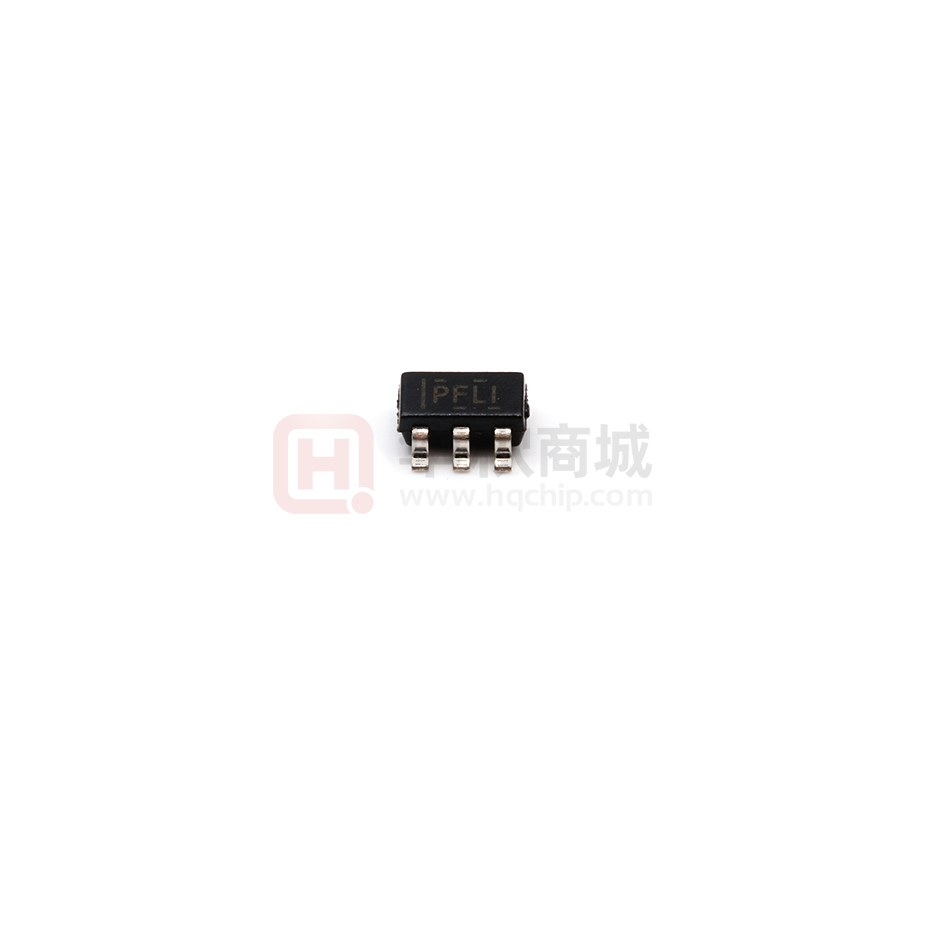
5 Device Comparison Table
PART NUMBER (1)
MARKING DBV
PACKAGE
TYPICAL FLYING CAPACITOR
[µF]
FEATURE
PFKI
1
Variable switching frequency 50 kHz-250 kHz
Fixed frequency 20 kHz
TPS60400DBV
TPS60401DBV
PFLI
10
TPS60402DBV
PFMI
3.3
Fixed frequency 50 kHz
TPS60403DBV
PFNI
1
Fixed frequency 250 kHz
(1)
The DBV package is available taped and reeled. Add R suffix to device type (for example, TPS60400DBVR) to order quantities of 3000
devices per reel. Add T suffix to device type (for example, TPS60400DBVT) to order quantities of 250 devices per reel.
6 Pin Configuration and Functions
DBV Package
5 Pins
Top View
OUT
1
IN
2
CFLY–
3
5
CFLY+
4
GND
Pin Functions
PIN
I/O
DESCRIPTION
NAME
NO.
CFLY+
5
Positive terminal of the flying capacitor C(fly)
CFLY-
3
Negative terminal of the flying capacitor C(fly)
GND
4
Ground
IN
2
I
Supply input. Connect to an input supply in the 1.6-V to 5.5-V range. Bypass IN to GND with a capacitor that
has the same value as the flying capacitor.
OUT
1
O
Power output with VO = -VI Bypass OUT to GND with the output filter capacitor CO.
7 Specifications
7.1 Absolute Maximum Ratings
over operating free-air temperature range (unless otherwise noted) (1)
Voltage
range
MIN
MAX
UNIT
IN to GND
-0.3
5.5
V
OUT to GND
-5.5
0.3
V
CFLY- to GND
0.3
VO - 0.3
V
CFLY+ to GND
-0.3 V
VI + 0.3
V
Continuous power dissipation
See Power Dissipation
Continuous output current
80
mA
Maximum junction temperature, TJ
150
°C
(1)
Stresses beyond those listed under Absolute Maximum Ratings may cause permanent damage to the device. These are stress ratings
only, and functional operation of the device at these or any other conditions beyond those indicated under Recommended Operating
Conditions is not implied. Exposure to absolute-maximum-rated conditions for extended periods may affect device reliability.
Copyright © 2001–2015, Texas Instruments Incorporated
Submit Documentation Feedback
Product Folder Links: TPS60400 TPS60401 TPS60402 TPS60403
3
�TPS60400, TPS60401
TPS60402, TPS60403
SLVS324B – JULY 2001 – REVISED APRIL 2015
www.ti.com
7.2 Handling Ratings
Tstg
V(ESD)
(1)
(2)
MIN
MAX
UNIT
-55°C
150°C
°C
Human body model (HBM), per ANSI/ESDA/JEDEC JS-001, all
pins (1)
-1000
1000
Charged device model (CDM), per JEDEC specification
JESD22-C101, all pins (2)
-500
500
Storage temperature range
Electrostatic discharge
V
JEDEC document JEP155 states that 500-V HBM allows safe manufacturing with a standard ESD control process.
JEDEC document JEP157 states that 250-V CDM allows safe manufacturing with a standard ESD control process.
7.3 Recommended Operating Conditions
MIN
Input voltage range, VI
NOM
1.8
MAX
5.25
Output current range at OUT, IO
60
Input capacitor, CI
0
C(fly)
Flying capacitor, C(fly)
1
Output capacitor, CO
1
Operating junction temperature, TJ
UNIT
-40
V
mA
µF
µF
100
µF
125
°C
7.4 Thermal Information
TPS6040x
THERMAL METRIC (1)
DBV
UNIT
5 PINS
RθJA
Junction-to-ambient thermal resistance
221.2
RθJC(top)
Junction-to-case (top) thermal resistance
81.9
RθJB
Junction-to-board thermal resistance
39.8
ψJT
Junction-to-top characterization parameter
3.3
ψJB
Junction-to-board characterization parameter
38.9
RθJC(bot)
Junction-to-case (bottom) thermal resistance
n/a
(1)
°C/W
For more information about traditional and new thermal metrics, see the IC Package Thermal Metrics application report, SPRA953.
7.5 Electrical Characteristics
CI = C(fly) = CO (according to Table 1), TC = -40°C to 85°C, VI = 5 V over recommended operating free-air temperature range
(unless otherwise noted)
PARAMETER
TEST CONDITIONS
VI
Supply voltage range
IO
Maximum output current at VO
VO
Output voltage
VP-P
1.8
At TC≥ 0°C, RL= 5 kΩ
1.6
TYP
TPS60400
C(fly) = 1 µF, CO = 2.2 µF
35
TPS60401
C(fly) = CO = 10 µF
20
C(fly) = CO = 3.3 µF
20
C(fly) = CO = 1 µF
15
TPS60402
Submit Documentation Feedback
IO = 5 mA
UNIT
V
mA
-VI
Output voltage ripple
MAX
5.25
60
TPS60403
4
MIN
At TC = -40°C to 85°C, RL = 5 kΩ
V
mVP-P
Copyright © 2001–2015, Texas Instruments Incorporated
Product Folder Links: TPS60400 TPS60401 TPS60402 TPS60403
�TPS60400, TPS60401
TPS60402, TPS60403
www.ti.com
SLVS324B – JULY 2001 – REVISED APRIL 2015
Electrical Characteristics (continued)
CI = C(fly) = CO (according to Table 1), TC = -40°C to 85°C, VI = 5 V over recommended operating free-air temperature range
(unless otherwise noted)
PARAMETER
TEST CONDITIONS
MIN
TPS60400
TPS60401
TPS60402
IQ
Quiescent current (no-load input
current)
At VI = 5 V
TPS60403
TYP
MAX
125
270
65
190
120
270
425
700
TPS60400
TPS60401
TPS60402
fOSC
Internal switching frequency
At T ≤ 60°C,
135
VI = 5 V
210
µA
640
30
50-250
350
TPS60401
VCO version
13
20
28
TPS60402
30
50
70
150
TPS60403
Impedance at 25°C, VI = 5 V
µA
210
TPS60403
TPS60400
UNIT
250
300
TPS60400
CI = C(fly) = CO = 1 µF
12
15
TPS60401
CI = C(fly) = CO = 10 µF
12
15
TPS60402
CI = C(fly) = CO = 3.3 µF
12
15
TPS60403
CI = C(fly) = CO = 1 µF
12
15
kHz
Ω
7.6 Typical Characteristics
Table 1. Table of Graphs
FIGURE
η
Efficiency
vs Output current at 3.3 V, 5 V
TPS60400, TPS60401, TPS60402, TPS60403
Figure 1,
Figure 2
II
Input current
vs Output current
TPS60400, TPS60401, TPS60402, TPS60403
Figure 3,
Figure 4
IS
Supply current
vs Input voltage
TPS60400, TPS60401, TPS60402, TPS60403
Figure 5,
Figure 6
Output resistance
vs Input voltage at -40°C, 0°C, 25°C, 85°C
TPS60400, CI = C(fly) = CO = 1 µF
TPS60401, CI = C(fly) = CO = 10 µF
TPS60402 , CI = C(fly) = CO = 3.3 µF
TPS60403, CI = C(fly) = CO = 1 µF
Figure 7,
Figure 8,
Figure 9,
Figure 10
VO
Output voltage
vs Output current at 25°C, VIN=1.8 V, 2.5 V, 3.3 V, 5 V
TPS60400, CI = C(fly) = CO = 1 µF
TPS60401, CI = C(fly) = CO = 10 µF
TPS60402 , CI = C(fly) = CO = 3.3 µF
TPS60403, CI = C(fly) = CO = 1 µF
Figure 11,
Figure 12,
Figure 13,
Figure 14
fOSC
Oscillator frequency
vs Temperature at VI = 1.8 V, 2.5 V, 3.3 V, 5 V
TPS60400, TPS60401, TPS60402, TPS60403
Figure 15,
Figure 16,
Figure 17,
Figure 18
fOSC
Oscillator frequency
vs Output current
TPS60400 at 2 V, 3.3 V, 5.0 V
Figure 19
Copyright © 2001–2015, Texas Instruments Incorporated
Submit Documentation Feedback
Product Folder Links: TPS60400 TPS60401 TPS60402 TPS60403
5
�TPS60400, TPS60401
TPS60402, TPS60403
SLVS324B – JULY 2001 – REVISED APRIL 2015
www.ti.com
100
100
TPS60400
VI = 5 V
95
TPS60402
VI = 5 V
90
85
Efficiency – %
90
Efficiency – %
TPS60403
VI = 5 V
95
TPS60401
VI = 5 V
TPS60401
VI = 3.3 V
80
75
TPS60400
VI = 3.3 V
70
85
80
TPS60403
VI = 3.3 V
75
TPS60402
VI = 3.3 V
70
65
65
TA = 25°C
60
0
10
20
30 40 50 60 70 80
IO – Output Current – mA
TA = 25°C
60
90 100
Figure 1. Efficiency vs Output Current
0
10
20
30 40 50 60 70 80
IO – Output Current – mA
90 100
Figure 2. Efficiency vs Output Current
100
100
TA = 25°C
TA = 25°C
I I – Input Current – mA
I I – Input Current – mA
TPS60400
VI = 5 V
10
TPS60401
VI = 5 V
TPS60401
VI = 2 V
1
TPS60403
VI = 5 V
10
TPS60403
VI = 2 V
1
TPS60402
VI = 5 V
TPS60400
VI = 2 V
0.1
0.1
TPS60402
VI = 2 V
1
10
IO – Output Current – mA
0.1
0.1
100
Figure 3. Input Current vs Output Current
1
10
IO – Output Current – mA
Figure 4. Input Current vs Output Current
0.6
0.6
IO = 0 mA
TA = 25°C
I DD – Supply Current – mA
IO = 0 mA
TA = 25°C
I DD – Supply Current – mA
100
0.4
0.2
0.4
TPS60403
0.2
TPS60400
TPS60402
TPS60401
0
0
1
2
3
VI – Input Voltage – V
4
0
5
Figure 5. Supply Current vs Input Voltage
6
Submit Documentation Feedback
0
1
2
3
VI – Input Voltage – V
4
5
Figure 6. Supply Current vs Input Voltage
Copyright © 2001–2015, Texas Instruments Incorporated
Product Folder Links: TPS60400 TPS60401 TPS60402 TPS60403
�TPS60400, TPS60401
TPS60402, TPS60403
www.ti.com
SLVS324B – JULY 2001 – REVISED APRIL 2015
40
40
IO = 30 mA
CI = C(fly) = CO = 1 µF
IO = 30 mA
CI = C(fly) = CO = 10 µF
35
30
30
ro – Output Resistance – W
ro – Output Resistance – W
35
25
TA = 85°C
20
TA = 25°C
15
10
25
20
TA = 25°C
TA = 85°C
15
10
5
5
TA = –40°C
TA = –40°C
0
1
2
3
4
VI – Input Voltage – V
5
0
6
Figure 7. Output Resistance vs Input Voltage
5
6
ro – Output Resistance – W
30
25
TA = 25°C
20
TA = 85°C
15
TA = –40°C
5
IO = 30 mA
CI = C(fly) = CO = 1 µF
35
10
30
25
20
TA = 25°C
TA = 85°C
15
10
5
0
TA = –40°C
0
1
2
3
4
VI – Input Voltage – V
5
6
Figure 9. Output Resistance vs Input Voltage
1
2
3
4
VI – Input Voltage – V
5
6
Figure 10. Output Resistance vs Input Voltage
0
0
TA = 25°C
–1
TA = 25°C
–1
VI = 1.8 V
VI = 1.8 V
VO – Output Voltage – V
VO – Output Voltage – V
3
4
VI – Input Voltage – V
40
IO = 30 mA
CI = C(fly) = CO = 3.3 µF
35
VI = 2.5 V
–2
–3
VI = 3.3 V
–4
VI = 5 V
–5
–6
2
Figure 8. Output Resistance vs Input Voltage
40
ro – Output Resistance – W
1
VI = 2.5 V
–2
VI = 3.3 V
–3
–4
VI = 5 V
–5
0
10
20
30
40
50
60
–6
0
10
20
30
40
50
60
IO – Output Current – mA
IO – Output Current – mA
Figure 11. Output Voltage vs Output Current
Figure 12. Output Voltage vs Output Current
Copyright © 2001–2015, Texas Instruments Incorporated
Submit Documentation Feedback
Product Folder Links: TPS60400 TPS60401 TPS60402 TPS60403
7
�TPS60400, TPS60401
TPS60402, TPS60403
SLVS324B – JULY 2001 – REVISED APRIL 2015
www.ti.com
0
0
TA = 25°C
TA = 25°C
–1
–1
VI = 1.8 V
VO – Output Voltage – V
VO – Output Voltage – V
VI = 1.8 V
VI = 2.5 V
–2
VI = 3.3 V
–3
–4
VI = 5 V
VI = 3.3 V
–3
–4
VI = 5 V
–5
–5
–6
VI = 2.5 V
–2
0
10
20
30
40
50
–6
60
0
10
20
30
40
50
60
IO – Output Current – mA
IO – Output Current – mA
Figure 13. Output Voltage vs Output Current
Figure 14. Output Voltage vs Output Current
24
250
23.8
VI = 1.8 V
200
150
VI = 2.5 V
VI = 3.3 V
100
VI = 5 V
50
f osc – Oscillator Frequency – kHz
f osc – Oscillator Frequency – kHz
IO = 10 mA
IO = 10 mA
23.6
VI = 3.3 V
23.4
VI = 5 V
23.2
23
VI = 2.5 V
22.8
22.6
VI = 1.8 V
22.4
22.2
0
–40 –30 –20 –10 0
22
–40 –30 –20 –10 0
10 20 30 40 50 60 70 80 90
TA – Free-Air Temperature – °C
Figure 15. Oscillator Frequency vs Free-Air Temperature
Figure 16. Oscillator Frequency vs Free-Air Temperature
250
57
IO = 10 mA
VI = 5 V
VI = 3.3 V
55
54
VI = 2.5 V
53
52
VI = 1.8 V
51
50
f osc – Oscillator Frequency – kHz
f osc – Oscillator Frequency – kHz
VI = 5 V
240
56
VI = 3.3 V
230
VI = 2.5 V
220
210
VI = 1.8 V
200
190
180
170
IO = 10 mA
160
49
–40 –30 –20 –10 0
8
10 20 30 40 50 60 70 80 90
TA – Free-Air Temperature – °C
10 20 30 40 50 60 70 80 90
150
–40 –30 –20 –10 0
10 20 30 40 50 60 70 80 90
TA – Free-Air Temperature – °C
TA – Free-Air Temperature – °C
Figure 17. Oscillator Frequency vs Free-Air Temperature
Figure 18. Oscillator Frequency vs Free-Air Temperature
Submit Documentation Feedback
Copyright © 2001–2015, Texas Instruments Incorporated
Product Folder Links: TPS60400 TPS60401 TPS60402 TPS60403
�TPS60400, TPS60401
TPS60402, TPS60403
www.ti.com
SLVS324B – JULY 2001 – REVISED APRIL 2015
300
f osc – Oscillator Frequency – kHz
TA = 25°C
VI = 3.3 V
250
VI = 1.8 V
200
VI = 5 V
150
100
50
0
0
10
20
30
40
50
60
70
80
90 100
IO – Output Current – mA
Figure 19. Oscillator Frequency vs Output Current
Copyright © 2001–2015, Texas Instruments Incorporated
Submit Documentation Feedback
Product Folder Links: TPS60400 TPS60401 TPS60402 TPS60403
9
�TPS60400, TPS60401
TPS60402, TPS60403
SLVS324B – JULY 2001 – REVISED APRIL 2015
www.ti.com
8 Detailed Description
8.1 Overview
The TPS60400, TPS60401 charge pumps invert the voltage applied to their input. For the highest performance,
use low equivalent series resistance (ESR) capacitors (for example, ceramic). During the first half-cycle, switches
S2 and S4 open, switches S1 and S3 close, and capacitor (C(fly)) charges to the voltage at VI. During the second
half-cycle, S1 and S3 open, S2 and S4 close. This connects the positive terminal of C(fly) to GND and the
negative to VO. By connecting C(fly) in parallel, CO is charged negative. The actual voltage at the output is more
positive than -VI, since switches S1-S4 have resistance and the load drains charge from CO.
VI
S1
C(fly)
S4
VO (–VI)
1 µF
S2
CO
1 µF
S3
GND
GND
Figure 20. Operating Principle
8.2 Functional Block Diagram
VI
VI – VCFLY+ < 0.5 V
VI
MEAS
VI < 1 V
VO > Vbe
R
Start
FF
S
Q
VO
DC_ Startup
VI
Q1
VO
MEAS
Q
OSC
CHG
OSC
50 kHz
Phase
Generator
+
Q
Q2
VO > –1 V
VI
B
Q3
Q5
GND
VO
DC_ Startup
VCO_CONT
VI / VO
MEAS
10
VO
Q4
C(fly)
VO < –VI – Vbe
Submit Documentation Feedback
Copyright © 2001–2015, Texas Instruments Incorporated
Product Folder Links: TPS60400 TPS60401 TPS60402 TPS60403
�TPS60400, TPS60401
TPS60402, TPS60403
www.ti.com
SLVS324B – JULY 2001 – REVISED APRIL 2015
8.3 Feature Description
8.3.1 Charge-Pump Output Resistance
The TPS6040x devices are not voltage regulators. The charge pump's output source resistance is approximately
15 Ω at room temperature (with VI = 5 V), and VO approaches -5 V when lightly loaded. VO droops toward GND
as load current increases.
VO = –(VI – RO × IO)
(1)
R
ǒ
1
Ǔ
) 4 2R
) ESR
) ESR
SWITCH
CFLY
CO
(fly)
RO = output resistance of the converter
O
[
ƒosc
C
(2)
8.3.2 Efficiency Considerations
The power efficiency of a switched-capacitor voltage converter is affected by three factors: the internal losses in
the converter IC, the resistive losses of the capacitors, and the conversion losses during charge transfer between
the capacitors. The internal losses are associated with the internal functions of the IC, such as driving the
switches, oscillator, and so forth. These losses are affected by operating conditions such as input voltage,
temperature, and frequency. The next two losses are associated with the output resistance of the voltage
converter circuit. Switch losses occur because of the on-resistance of the MOSFET switches in the IC. Chargepump capacitor losses occur because of their ESR. The relationship between these losses and the output
resistance is as follows:
PCAPACITOR LOSSES + PCONVERSION LOSSES = IO2 × RO
RSWITCH = resistance of a single MOSFET-switch inside the converter
fOSC = oscillator frequency
(3)
The first term is the effective resistance from an ideal switched-capacitor circuit. Conversion losses occur during
the charge transfer between C(fly) and CO when there is a voltage difference between them. The power loss is:
P CONV.LOSS + 1 C (fly) VI2 * VO2 ) 1 C O VRIPPLE2 * 2VOV RIPPLE
ƒ osc
2
2
(4)
ƪ
ǒ
Ǔ
ǒ
Ǔƫ
The efficiency of the TPS6040x devices is dominated by their quiescent supply current at low output current and
by their output impedance at higher current.
h^
IO
IO ) I Q
ǒ
I
1* O
Ǔ
RO
VI
(5)
Where, IQ = quiescent current.
Copyright © 2001–2015, Texas Instruments Incorporated
Submit Documentation Feedback
Product Folder Links: TPS60400 TPS60401 TPS60402 TPS60403
11
�TPS60400, TPS60401
TPS60402, TPS60403
SLVS324B – JULY 2001 – REVISED APRIL 2015
www.ti.com
8.4 Device Functional Modes
8.4.1 Active-Schottky Diode
For a short period of time, when the input voltage is applied, but the inverter is not yet working, the output
capacitor is charged positive by the load. To prevent the output being pulled above GND, a Schottky diode must
be added in parallel to the output. The function of this diode is integrated into the TPS6040x devices, which gives
a defined startup performance and saves board space.
A current sink and a diode in series can approximate the behavior of a typical, modern operational amplifier.
Figure 21 shows the current into this typical load at a given voltage. The TPS6040x devices are optimized to
start into these loads.
VI
C(fly)
5
1 µF
+V
Typical
Load
3
-V
C1+
C1TPS60400
2
OUT VO (-VI)
1
IO
IN
CI
1 µF
CO
1 µF
GND
4
GND
Figure 21. Typical Load
Load Current
60 mA
0.4 V
25 mA
0.4 V 1.25 V
5V
Voltage at the Load
Figure 22. Maximum Start-Up Current
12
Submit Documentation Feedback
Copyright © 2001–2015, Texas Instruments Incorporated
Product Folder Links: TPS60400 TPS60401 TPS60402 TPS60403
�TPS60400, TPS60401
TPS60402, TPS60403
www.ti.com
SLVS324B – JULY 2001 – REVISED APRIL 2015
9 Application and Implementation
NOTE
Information in the following applications sections is not part of the TI component
specification, and TI does not warrant its accuracy or completeness. TI’s customers are
responsible for determining suitability of components for their purposes. Customers should
validate and test their design implementation to confirm system functionality.
9.1 Application Information
The TPS6040x is a family of devices that generate an unregulated negative output voltage from an input voltage
ranging from 1.6 V to 5.5 V.
9.2 Typical Application
9.2.1 Voltage Inverter
The design guidelines provide a component selection to operate the device within the recommended operating
conditions.
C(fly)
2
Input 5 V
CI
1 µF
1 µF
3
5
C1–
C1+
TPS60400
IN
OUT
GND
4
1
CO
1 µF
–5 V,
Max 60 mA
Figure 23. Typical Operating Circuit
9.2.1.1 Design Requirements
The TPS6040x is connected to generate a negative output voltage from a positive input.
9.2.1.2 Detailed Design Procedure
The most common application for these devices is a charge-pump voltage inverter (see Figure 23). This
application requires only two external components; capacitors C(fly) and CO, plus a bypass capacitor, if
necessary. Refer to the capacitor selection section for suggested capacitor types.
For the maximum output current and best performance, three ceramic capacitors of 1 µF (TPS60400, TPS60403)
are recommended. For lower currents or higher allowed output voltage ripple, other capacitors can also be used.
It is recommended that the output capacitors has a minimum value of 1 µF. With flying capacitors lower than 1
µF, the maximum output power decreases.
9.2.1.2.1 Capacitor Selection
To maintain the lowest output resistance, use capacitors with low ESR (see Table 2). The charge-pump output
resistance is a function of C(fly)'s and CO's ESR. Therefore, minimizing the charge-pump capacitor's ESR
minimizes the total output resistance. The capacitor values are closely linked to the required output current and
the output noise and ripple requirements. It is possible to only use 1-µF capacitors of the same type.
9.2.1.2.2
Input Capacitor (CI)
Bypass the incoming supply to reduce its ac impedance and the impact of the TPS6040x switching noise. The
recommended bypassing depends on the circuit configuration and where the load is connected. When the
inverter is loaded from OUT to GND, current from the supply switches between 2 x IO and zero. Therefore, use a
large bypass capacitor (for example, equal to the value of C(fly)) if the supply has high ac impedance. When the
inverter is loaded from IN to OUT, the circuit draws 2 × IO constantly, except for short switching spikes. A 0.1-µF
bypass capacitor is sufficient.
Copyright © 2001–2015, Texas Instruments Incorporated
Submit Documentation Feedback
Product Folder Links: TPS60400 TPS60401 TPS60402 TPS60403
13
�TPS60400, TPS60401
TPS60402, TPS60403
SLVS324B – JULY 2001 – REVISED APRIL 2015
www.ti.com
Typical Application (continued)
9.2.1.2.3
Flying Capacitor (C(fly))
Increasing the flying capacitor's size reduces the output resistance. Small values increases the output resistance.
Above a certain point, increasing C(fly)'s capacitance has a negligible effect, because the output resistance
becomes dominated by the internal switch resistance and capacitor ESR.
9.2.1.2.4
Output Capacitor (CO)
Increasing the output capacitor's size reduces the output ripple voltage. Decreasing its ESR reduces both output
resistance and ripple. Smaller capacitance values can be used with light loads if higher output ripple can be
tolerated. Use the following equation to calculate the peak-to-peak ripple.
I
O
V
+
)2 I
ESR
O(ripple)
O
CO
f osc Co
(6)
Table 2. Recommended Capacitor Values
DEVICE
VI
[V]
IO
[mA]
CI
[µF]
C(fly)
[µF]
CO
[µF]
TPS60400
1.8…5.5
60
1
1
1
TPS60401
1.8…5.5
60
10
10
10
TPS60402
1.8…5.5
60
3.3
3.3
3.3
TPS60403
1.8…5.5
60
1
1
1
Table 3. Recommended Capacitors
MANUFACTURER
PART NUMBER
SIZE
CAPACITANCE
TYPE
Taiyo Yuden
EMK212BJ474MG
0805
0.47 µF
Ceramic
LMK212BJ105KG
0805
1 µF
Ceramic
LMK212BJ225MG
0805
2.2 µF
Ceramic
EMK316BJ225KL
1206
2.2 µF
Ceramic
LMK316BJ475KL
1206
4.7 µF
Ceramic
TDK
JMK316BJ106KL
1206
10 µF
Ceramic
C2012X5R1C105M
0805
1 µF
Ceramic
C2012X5R1A225M
0805
2.2 µF
Ceramic
C2012X5R1A335M
0805
3.3 µF
Ceramic
Table 4 contains a list of manufacturers of the recommended capacitors. Ceramic capacitors will provide the
lowest output voltage ripple because they typically have the lowest ESR-rating.
Table 4. Recommended Capacitor Manufacturers
14
CAPACITOR TYPE
MANUFACTURER
WEB ADDRESS
X5R / X7R ceramic
Taiyo Yuden
www.t-yuden.com
X5R / X7R ceramic
TDK
www.component.tdk.com
X5R / X7R ceramic
Vishay
www.vishay.com
X5R / X7R ceramic
Kemet
www.kemet.com
Submit Documentation Feedback
Copyright © 2001–2015, Texas Instruments Incorporated
Product Folder Links: TPS60400 TPS60401 TPS60402 TPS60403
�TPS60400, TPS60401
TPS60402, TPS60403
www.ti.com
SLVS324B – JULY 2001 – REVISED APRIL 2015
9.2.1.2.5 Power Dissipation
As given in the Thermal Information, the thermal resistance of TPS6040x is: RΘJA = 221°C/W.
The terminal resistance can be calculated using the following equation:
T *T
A
R
+ J
qJA
P
D
(7)
where:
TJ is the junction temperature. TA is the ambient temperature. PD is the power that is dissipated by the
device.
T *T
A
R
+ J
qJA
P
D
(8)
The maximum power dissipation can be calculated using the following equation:
PD = VI× II - VO× IO = VI(max)× (IO + I(SUPPLY)) - VO× IO
(9)
The maximum power dissipation happens with maximum input voltage and maximum output current.
At maximum load the supply current is 0.7 mA maximum.
PD = 5 V × (60 mA + 0.7 mA) - 4.4 V × 60 mA = 40 mW
(10)
With this maximum rating and the thermal resistance of the device on the EVM, the maximum temperature rise
above ambient temperature can be calculated using the following equation:
ΔTJ = RΘJA× PD = 221°C/W × 40 mW =8.8°C
(11)
This means that the internal dissipation increases TJ by