Product
Folder
Sample &
Buy
Support &
Community
Tools &
Software
Technical
Documents
TPS61097A-33
SLVSCF2A – JANUARY 2014 – REVISED DECEMBER 2014
TPS61097A-33 Low-Input Voltage Synchronous-Boost Converter With Low Quiescent
Current
1 Features
3 Description
•
The TPS61097A-33 provides a power supply solution
for products powered by either a single-cell, two-cell,
or three-cell alkaline, NiCd, or NiMH, or one-cell LiIon or Li-polymer battery. They can also be used in
fuel cell or solar cell powered devices where the
capability of handling low input voltages is essential.
Possible output currents depend on the input-tooutput voltage ratio. The devices provide output
currents up to 100 mA at a 3.3-V output while using a
single-cell Li-Ion or Li-Polymer battery. The boost
converter is based on a current-mode controller using
synchronous rectification to obtain maximum
efficiency. The maximum average input current is
limited to a value of 400 mA. The converter can be
disabled to minimize battery drain. During shutdown,
the battery is connected to the load to enable battery
backup of critical functions on the load. The device is
packaged in a 5-pin SOT-23 package (DBV)
measuring 2.8 mm × 2.9 mm.
1
•
•
•
•
•
•
•
Up to 93% Efficiency at Typical Operating
Conditions
Connection from Battery to Load via Bypass
Switch in Shutdown Mode
Typical Shutdown Current Less Than 5 nA
Typical Quiescent Current Less Than 5 μA
Operating Input Voltage Range
From 0.9 V to 5.5 V
Power-Save Mode for Improved Efficiency at Low
Output Power
Overtemperature Protection
Small 2.8-mm x 2.9-mm 5-Pin SOT-23 Package
2 Applications
•
•
•
•
•
•
•
MSP430 Applications
All Single-Cell, Two-Cell, and Three-Cell Alkaline,
NiCd, NiMH, or Single-Cell Li-Battery Powered
Products
Personal Medical Products
Fuel Cell and Solar Cell Powered Products
PDAs
Mobile Applications
White LEDs
Device Information(1)
PART NUMBER
TPS61097A-33
PACKAGE
BODY SIZE (NOM)
SOT-23 (5)
2.90 mm × 2.90 mm
(1) For all available packages, see the orderable addendum at
the end of the datasheet.
Typical Operating Application
L1
L
TPS61097A
VOUT
VOUT
+3.3V
C2
VIN
0.9 V to 3.3V
VIN
C1
EN
GND
1
An IMPORTANT NOTICE at the end of this data sheet addresses availability, warranty, changes, use in safety-critical applications,
intellectual property matters and other important disclaimers. PRODUCTION DATA.
�TPS61097A-33
SLVSCF2A – JANUARY 2014 – REVISED DECEMBER 2014
www.ti.com
Table of Contents
1
2
3
4
5
6
7
8
Features ..................................................................
Applications ...........................................................
Description .............................................................
Revision History.....................................................
Pin Configuration and Functions .........................
Specifications.........................................................
1
1
1
2
3
3
6.1
6.2
6.3
6.4
6.5
6.6
3
3
3
4
4
5
Absolute Maximum Ratings ......................................
ESD Ratings..............................................................
Recommended Operating Conditions.......................
Thermal Information ..................................................
Electrical Characteristics...........................................
Typical Characteristics ..............................................
Parameter Measurement Information .................. 8
Detailed Description .............................................. 9
8.1 Overview ................................................................... 9
8.2 Functional Block Diagram ......................................... 9
8.3 Feature Description................................................. 10
8.4 Device Functional Modes........................................ 11
9
Application and Implementation ........................ 12
9.1 Application Information............................................ 12
9.2 Typical Application .................................................. 13
10 Power Supply Recommendations ..................... 16
11 Layout................................................................... 16
11.1 Layout Guidelines ................................................. 16
11.2 Layout Example .................................................... 16
12 Device and Documentation Support ................. 17
12.1
12.2
12.3
12.4
Device Support ....................................................
Trademarks ...........................................................
Electrostatic Discharge Caution ............................
Glossary ................................................................
17
17
17
17
13 Mechanical, Packaging, and Orderable
Information ........................................................... 17
4 Revision History
Changes from Original (January 2014) to Revision A
•
2
Page
Added Handling Rating table, Feature Description section, Device Functional Modes, Application and
Implementation section, Power Supply Recommendations section, Layout section, Device and Documentation
Support section, and Mechanical, Packaging, and Orderable Information section ............................................................... 1
Submit Documentation Feedback
Copyright © 2014, Texas Instruments Incorporated
�TPS61097A-33
www.ti.com
SLVSCF2A – JANUARY 2014 – REVISED DECEMBER 2014
5 Pin Configuration and Functions
FIXED OUTPUT VOLTAGE
DBV PACKAGE
(TOP VIEW)
VIN
1
GND
2
EN
3
5
L
4
VOUT
Pin Functions
PIN
NO.
NAME
I/O
DESCRIPTION
1
VIN
I
Boost converter input voltage.
2
GND
–
Control / logic ground.
3
EN
I
Enable input (1 = enabled, 0 = disabled). EN must be actively terminated high or low.
4
VOUT
O
Boost converter output.
5
L
I
Connection for inductor.
6 Specifications
6.1 Absolute Maximum Ratings
Over operating free-air temperature range (unless otherwise noted) (1)
VI
Input voltage range
MIN
MAX
VIN
–0.3
7
L
–0.3
7
VOUT
–0.3
7
EN
–0.3
7
UNIT
V
IMAX
Maximum continuous output current
400
mA
TJ
Junction temperature range
–40
150
°C
Tstg
Storage temperature range
–65
150
°C
(1)
Stresses beyond those listed under Absolute Maximum Ratings may cause permanent damage to the device. These are stress ratings
only, and functional operation of the device at these or any other conditions beyond those indicated under Recommended Operating
Conditions is not implied. Exposure to absolute-maximum-rated conditions for extended periods may affect device reliability.
6.2 ESD Ratings
VALUE
V(ESD)
(1)
(2)
Electrostatic discharge
Human-body model (HBM), per ANSI/ESDA/JEDEC JS-001 (1)
±2000
Charged-device model (CDM), per JEDEC specification JESD22C101 (2)
±1000
UNIT
V
JEDEC document JEP155 states that 500-V HBM allows safe manufacturing with a standard ESD control process.
JEDEC document JEP157 states that 250-V CDM allows safe manufacturing with a standard ESD control process.
6.3 Recommended Operating Conditions
MIN
MAX
UNIT
0.9
5.5
0
5.5
V
VIN
Input voltage range
VEN
Enable voltage range
TA
Operating free air temperature range
–40
85
°C
TJ
Operating junction temperature range
–40
125
°C
Copyright © 2014, Texas Instruments Incorporated
Submit Documentation Feedback
V
3
�TPS61097A-33
SLVSCF2A – JANUARY 2014 – REVISED DECEMBER 2014
www.ti.com
6.4 Thermal Information
TPS61097A-33
THERMAL METRIC (1)
DBV
UNIT
5 PINS
θJA
Junction-to-ambient thermal resistance
208.7
θJCtop
Junction-to-case (top) thermal resistance
124.5
θJB
Junction-to-board thermal resistance
36.9
ψJT
Junction-to-top characterization parameter
14.7
ψJB
Junction-to-board characterization parameter
(1)
°C/W
36
For more information about traditional and new thermal metrics, see the IC Package Thermal Metrics application report, SPRA953.
6.5 Electrical Characteristics
Over recommended free-air temperature range and over recommended input voltage range (typical at an ambient
temperature range of 25°C) (unless otherwise noted)
PARAMETER
TEST CONDITIONS
MIN
TYP
MAX
UNIT
DC/DC STAGE
VIN
Input voltage
VOUT
Output voltage
VIN = 1.2 V , IOUT = 10 mA
3.20
3.30
3.40
ISW
Switch current limit
VOUT = 3.3 V
200
400
475
Rectifying switch on resistance
VOUT = 3.3 V
1.0
Main switch on resistance
VOUT = 3.3 V
1.0
Bypass switch on resistance
VIN = 1.2 IOUT = 100 mA
3.4
Line regulation
VIN < VOUT, VIN = 1.2 V to 1.8 V, IOUT = 10 mA
0.5%
Load regulation
VIN < VOUT, IOUT = 10 mA to 50 mA, VIN = 1.8 V
0.5%
IQ
Quiescent current
ISD
Shutdown current
0.9
VIN
VOUT
VIN
Leakage current into L
5.5
mA
Ω
2
4
5
8
VEN = 0 V, VIN = 1.2 V, IOUT = 0 mA
0.005
0.15
VEN = 0 V, VIN = 3 V, IOUT = 0 mA
0.005
0.15
VEN = 0 V, VIN = 1.2 V, VL = 1.2 V
0.01
1
EN = 0 V or EN = VIN
0.01
IOUT = 0 mA, VEN = VIN = 1.2 V, VOUT = 3.5 V
V
μA
μA
CONTROL STAGE
EN input current
VIL
Logic low level, EN falling edge
VIH
Logic high level, EN rising edge
OTP
Overtemperature protection
150
OTPHYST
Overtemperature hysteresis
20
VUVLO
Undervoltage lock-out threshold
for turn off
4
Submit Documentation Feedback
0.1
μA
0.58
VIN +
1.0 V
0.78
VIN decreasing
0.6
V
°C
0.8
V
Copyright © 2014, Texas Instruments Incorporated
�TPS61097A-33
www.ti.com
SLVSCF2A – JANUARY 2014 – REVISED DECEMBER 2014
6.6 Typical Characteristics
Refer to Figure 19 for reference designators.
0.3
100
90
0.25
80
70
0.2
Efficiency - %
IOUT(MAX) - Maximum Output Current - A
C2 = 10µF, ceramic
L = 10µH
0.15
60
50
40
VIN = 0.9V
0.1
VIN = 1.2V
30
VIN = 1.5V
20
0.05
VIN = 1.8V
VIN = 2.5V
10
VIN = 3.0V
0
C2 = 10µF, ceramic
L = 10µH
0
0.9
1.2
1.5
1.8
2.1
2.4
2.7
3
1
10
VIN - Input Voltage - V
100
IOUT - Output Current - mA
C001
C002
Figure 1. Maximum Output Current vs Input Voltage
Figure 2. Efficiency vs Output current
100
6
Device Enabled
No Output Load
VOUT = 3.3V
90
5
80
IIN - Input Current - µA
Efficiency - %
70
60
50
40
IOUT = 1mA
30
4
3
2
IOUT = 5mA
20
IOUT = 10mA
10
1
IOUT = 50mA
C2 = 10µF, ceramic
L = 10µH
IOUT = 100mA
0
0
0.9
1.2
1.5
1.8
2.1
2.4
2.7
3
0.9
1.2
1.5
1.8
VIN - Input Voltage - V
2.1
2.4
2.7
3
3.3
3.6
3.9
4.2
VIN - Input Voltage -V
C003
C004
Figure 3. Efficiency vs Input Voltage
Figure 4. Input Current vs Input Voltage
120
0.7
Device Disabled
No Output Load
Temperature = 25£C
100
0.696
VIH - Logic High Level - V
IIN - Input Current - nA
VIN = 1.8V
No Output Load
0.698
80
60
40
0.694
0.692
0.69
0.688
0.686
0.684
20
0.682
0.68
0
0.9
1.2
1.5
1.8
2.1
2.4
2.7
3
3.3
3.6
3.9
4.2
-40
-25
-10
5
20
35
50
65
C006
C004
Figure 5. Input Current vs Input Voltage
Copyright © 2014, Texas Instruments Incorporated
80
Temperature - oC
VIN - Input Voltage -V
Figure 6. VIH vs Temperature
Submit Documentation Feedback
5
�TPS61097A-33
SLVSCF2A – JANUARY 2014 – REVISED DECEMBER 2014
www.ti.com
Typical Characteristics (continued)
0.725
3.40
VIN = 1.8V
Temperature = 25£C
0.72
3.36
VOUT - Output Voltage - V
VIH - Logic High Level - V
C2 = 10µF, ceramic
L = 10µH
3.38
0.715
0.71
0.705
3.34
3.32
3.30
3.28
VIN = 0.9V
VIN = 1.2V
3.26
VIN = 1.5V
VIN = 1.8V
3.24
VIN = 2.1V
3.22
0.7
VIN = 2.5V
VIN = 3.0V
3.20
1
10
100
1
IOUT - Output Current - mA
10
100
1000
IOUT - Output Current - mA
C007
Figure 7. VIH vs Output Current
C008
Figure 8. Output Voltage vs Output Current
6
RLOAD = 122
Device Disabled
RLOAD = 1k
VOUT - Output Voltage - V
5
4
3
2
1
0
0
1
2
3
4
5
6
VIN - Input Voltage -V
C009
Figure 9. Output Voltage vs Input Voltage
Figure 10. Output Voltage Ripple
VIN = 1.8 V to 2.4 V
RLOAD = 100Ω
*VIN offset of 1.8V
Figure 11. Load Transient Response
6
Submit Documentation Feedback
Figure 12. Line Transient Response
Copyright © 2014, Texas Instruments Incorporated
�TPS61097A-33
www.ti.com
SLVSCF2A – JANUARY 2014 – REVISED DECEMBER 2014
Typical Characteristics (continued)
Figure 13. Switching Waveform, Continuous Mode
Copyright © 2014, Texas Instruments Incorporated
Figure 14. Switching Waveform, Discontinuous Mode
Submit Documentation Feedback
7
�TPS61097A-33
SLVSCF2A – JANUARY 2014 – REVISED DECEMBER 2014
www.ti.com
7 Parameter Measurement Information
Figure 15. Measurement Test Circuit
Table 1. List of Components
8
REFERENCE
MANUFACTURER
PART NO.
C2
Murata
GRM319R61A106KE19 10μF 10V X5R 1206 20%
C3
Murata
GRM319R61A106KE19 10μF 10V X5R 1206 20%
L1
Coilcraft
DO3314-103MLC
Submit Documentation Feedback
Copyright © 2014, Texas Instruments Incorporated
�TPS61097A-33
www.ti.com
SLVSCF2A – JANUARY 2014 – REVISED DECEMBER 2014
8 Detailed Description
8.1 Overview
The TPS61097A-33 is a high performance, high efficiency switching boost converter. To achieve high efficiency
the power stage is realized as a synchronous boost topology. For the power switching, two actively controlled low
RDSon power MOSFETs are implemented.
8.2 Functional Block Diagram
Bypass
Switch
P
N
L
VOUT
Rectifying
Switch
Thermal Shutdown
Startup Circuit
N
Driver
VIN
Undervoltage
Lockout
Bypass Switch
Control
Main
Switch
Control Logic
Current
Sense
EN
Overvoltage
Protection
GND
1.20 V
Copyright © 2014, Texas Instruments Incorporated
Submit Documentation Feedback
9
�TPS61097A-33
SLVSCF2A – JANUARY 2014 – REVISED DECEMBER 2014
www.ti.com
8.3 Feature Description
8.3.1
Controller Circuit
The device is controlled by a hysteretic current mode controller. This controller regulates the output voltage by
keeping the inductor ripple current constant in the range of 200 mA and adjusting the offset of this inductor
current depending on the output load. If the required average input current is lower than the average inductor
current defined by this constant ripple the inductor current goes discontinuous to keep the efficiency high at low
load conditions.
IL
Continuous Current Operation
Discontinuous Current Operation
200 mA
(typ.)
200 mA
(typ.)
t
Figure 16. Hysteretic Current Operation
The output voltage VOUT is monitored via the feedback network which is connected to the voltage error amplifier.
To regulate the output voltage, the voltage error amplifier compares this feedback voltage to the internal voltage
reference and adjusts the required offset of the inductor current accordingly.
8.3.2 Device Enable and Shutdown Mode
The device is enabled when EN is set high and shut down when EN is low. During shutdown, the converter stops
switching and all internal control circuitry is turned off.
8.3.3 Bypass Switch
The TPS61097A-33 contains a P-channel MOSFET (Bypass Switch) in parallel with the synchronous rectifying
MOSFET. When the IC is enabled (VEN > VIH), the Bypass Switch is turned off to allow the IC to work as a
standard boost converter. When the IC is disabled (VEN < VIL) the Bypass Switch is turned on to provide a direct,
low impedance connection from the input voltage (at the L pin) to the load (VOUT). The Bypass Switch is not
impacted by Undervoltage lockout, Overvoltage or Thermal shutdown.
8.3.4 Startup
After the EN pin is tied high, the device starts to operate. If the input voltage is not high enough to supply the
control circuit properly a startup oscillator starts to operate the switches. During this phase the switching
frequency is controlled by the oscillator and the maximum switch current is limited. As soon as the device has
built up the output voltage to about 1.8 V, high enough for supplying the control circuit, the device switches to its
normal hysteretic current mode operation. The startup time depends on input voltage and load current.
8.3.5 Operation at Output Overload
If in normal boost operation the inductor current reaches the internal switch current limit threshold the main
switch is turned off to stop further increase of the input current. In this case the output voltage will decrease since
the device can not provide sufficient power to maintain the set output voltage.
If the output voltage drops below the input voltage the backgate diode of the rectifying switch gets forward biased
and current starts flow through it. Because this diode cannot be turned off, the load current is only limited by the
remaining DC resistances. As soon as the overload condition is removed, the converter automatically resumes
normal operation and enters the appropriate soft start mode depending on the operating conditions.
8.3.6 Undervoltage Lockout
An undervoltage lockout function stops the operation of the converter if the input voltage drops below the typical
undervoltage lockout threshold. This function is implemented in order to prevent malfunctioning of the converter.
The undervoltage lockout function has no control of the Bypass Switch. If the Bypass Switch is enabled
(VEN < VIL) there is no impact during an undervoltage condition, and the Bypass Switch remains on.
10
Submit Documentation Feedback
Copyright © 2014, Texas Instruments Incorporated
�TPS61097A-33
www.ti.com
SLVSCF2A – JANUARY 2014 – REVISED DECEMBER 2014
Feature Description (continued)
8.3.7 Overtemperature Protection
The device has a built-in temperature sensor which monitors the internal IC temperature. If the temperature
exceeds the programmed threshold (OTP), the device stops operating. As soon as the IC temperature has
decreased below the programmed threshold (OTP - OTP HYST), it starts operating again. There is a built-in
hysteresis to avoid unstable operation at IC temperatures at the overtemperature threshold.
8.4 Device Functional Modes
Copyright © 2014, Texas Instruments Incorporated
EN
DEVICE STATE
H
Boost Converter
L
Bypass Switch
Submit Documentation Feedback
11
�TPS61097A-33
SLVSCF2A – JANUARY 2014 – REVISED DECEMBER 2014
www.ti.com
9 Application and Implementation
NOTE
Information in the following applications sections is not part of the TI component
specification, and TI does not warrant its accuracy or completeness. TI’s customers are
responsible for determining suitability of components for their purposes. Customers should
validate and test their design implementation to confirm system functionality.
9.1 Application Information
9.1.1 Adjustable Bypass Switching
The EN pin can be set up as a low voltage control for the bypass switch. By setting the desired ratio of R1 and
R2, the TPS61097A-33 can be set to switch on the bypass at a defined voltage level on VIN. For example,
setting R1 and R2 to 200 KΩ would set VEN to half of VIN. The voltage level of VIN engaging the bypass switch
is based on the VIL level of EN (0.58 V). If VIN is less than 1.16 V then the bypass switch will be enabled. For
VIN values above 1.56 V (50% of VIH) the bypass switch is disabled.
TPS61097A-33
L1
L
VOUT
+3.3V
VOUT
C2
VIN
0.9 V to 3.3V
VIN
C1
R1
EN
R2
GND
Figure 17. Adjustable Bypass Switching
9.1.2 Managing Inrush Current
Upon startup, the output capacitor of the boost converter can act as a virtual short circuit. The amount of inrush
current is dependent on the rate of increase of the input voltage, the inductance used with the converter, the
output capacitance and the parasitic circuit resistance. One method to reduce the inrush current is to use a load
switch with controlled turn-on. Texas Instruments has a large offering of controlled slew rate load switches which
can be found at www.ti.com/loadswitches. Below is an example circuit that has a load switch with controlled turnon.
TPS61097A VOUT
L
VOUT
+3.3V
L1
TPS22920L
C2
VIN
VIN
VIN
VOUT
0.9V to 3.3V
R1
C1
EN
GND
EN
R2
GND
Figure 18. Example Circuit with Load Switch
12
Submit Documentation Feedback
Copyright © 2014, Texas Instruments Incorporated
�TPS61097A-33
www.ti.com
SLVSCF2A – JANUARY 2014 – REVISED DECEMBER 2014
Application Information (continued)
9.1.3 Thermal Considerations
Implementation of integrated circuits in low-profile and fine-pitch surface-mount packages typically requires
special attention to power dissipation. Many system-dependent issues such as thermal coupling, airflow, added
heat sinks and convection surfaces, and the presence of other heat-generating components affect the powerdissipation limits of a given component.
Three basic approaches for enhancing thermal performance are listed below.
• Improving the power dissipation capability of the PCB design
• Improving the thermal coupling of the component to the PCB
• Introducing airflow in the system
The maximum recommended junction temperature (TJ) of the TPS61097A-33 devices is 125°C. Specified
regulator operation is assured to a maximum ambient temperature TA of 85°C. Therefore, the maximum power
dissipation is about 191.7 mW. More power can be dissipated if the maximum ambient temperature of the
application is lower.
9.2 Typical Application
Figure 19. Typical Application Schematic
9.2.1 Design Requirements
DESIGN PARAMETERS
EXAMPLE VALUE
Input Voltage (VIN)
1.2 V to 1.8 V
Output Voltage (VOUT)
3.3 V
Output Current (IOUT)
10 mA
9.2.2 Detailed Design Procedure
9.2.2.1 Inductor Selection
To make sure that the TPS61097A-33 devices can operate, a suitable inductor must be connected between pin
VIN and pin L. Inductor values of 4.7 μH show good performance over the whole input and output voltage range .
Choosing other inductance values affects the switching frequency f proportional to 1/L as shown in Equation 1.
L=
V ´ (VOUT - VIN )
1
´ IN
f ´ 200 mA
VOUT
Copyright © 2014, Texas Instruments Incorporated
(1)
Submit Documentation Feedback
13
�TPS61097A-33
SLVSCF2A – JANUARY 2014 – REVISED DECEMBER 2014
www.ti.com
Choosing inductor values higher than 4.7 μH can improve efficiency due to reduced switching frequency and
therefore with reduced switching losses. Using inductor values below 2.2 μH is not recommended.
Having selected an inductance value, the peak current for the inductor in steady state operation can be
calculated. Equation 2 gives the peak current estimate.
IL,MAX
ì VOUT ´ IOUT
+ 100 mA; continous current operation
ï
= í 0.8 ´ VIN
ï200 mA;
discontinuous current operation
î
(2)
IL,MAX is the inductor's required minimum current rating. Note that load transient or over current conditions may
require an even higher current rating.
Equation 3 provides an easy way to estimate whether the device is operating in continuous or discontinuous
operation. As long as the equation is true, continuous operation is typically established. If the equation becomes
false, discontinuous operation is typically established.
VOUT ´ IOUT
> 0.8 ´ 100 mA
VIN
(3)
Due to the use of current hysteretic control in the TPS61097A-33, the series resistance of the inductor can
impact the operation of the main switch. There is a simple calculation that can ensure proper operation of the
TPS61097A-33 boost converter. The relationship between the series resistance (RIN), the input voltage (VIN) and
the switch current limit (ISW) is shown in Equation 4.
RIN < VIN / ISW
(4)
Examples:
ISW = 400 mA, VIN = 2.5 V
(5)
In Equation 5, RIN < 2.5 V / 400 mA; therefore, RIN must be less than 6.25 Ω.
ISW = 400 mA, VIN = 1.8 V
(6)
In Equation 6, RIN < 1.8 V / 400 mA; therefore, RIN must be less than 4.5 Ω.
The following inductor series from different suppliers have been used with TPS61097A-33 converters:
Table 2. List of Inductors
VENDOR
INDUCTOR SERIES
Coilcraft
DO3314
TDK
NLC565050T
Taiyo Yuden
CBC2012T
9.2.2.2 Capacitor Selection
9.2.2.2.1
Input Capacitor
The input capacitor should be at least 10-μF to improve transient behavior of the regulator and EMI behavior of
the total power supply circuit. The input capacitor should be a ceramic capacitor and be placed as close as
possible to the VIN and GND pins of the IC.
9.2.2.2.2
Output Capacitor
For the output capacitor C2 , it is recommended to use small ceramic capacitors placed as close as possible to
the VOUT and GND pins of the IC. If, for any reason, the application requires the use of large capacitors which
can not be placed close to the IC, the use of a small ceramic capacitor with a capacitance value of around 2.2 μF
in parallel to the large one is recommended. This small capacitor should be placed as close as possible to the
VOUT and GND pins of the IC.
A minimum capacitance value of 4.7 μF should be used, 10 μF are recommended. If the inductor exceeds 4.7
μH, the value of the output capacitance value needs to be half the inductance value or higher for stability
reasons, see Equation 7.
14
Submit Documentation Feedback
Copyright © 2014, Texas Instruments Incorporated
�TPS61097A-33
www.ti.com
C2 ³
SLVSCF2A – JANUARY 2014 – REVISED DECEMBER 2014
L
´
2
(7)
Using low ESR capacitors, such as ceramic capacitors, is recommended to minimize output voltage ripple. If
heavy load changes are expected, the output capacitor value should be increased to avoid output voltage drops
during fast load transients.
Table 3. Recommended Output Capacitors
VENDOR
CAPACITOR SERIES
Murata
GRM188R60J106M47D 10μF 6.3V X5R 0603
Murata
GRM319R61A106KE19 10μF 10V X5R 1206
9.2.3 Application Curves
VIN = 1.2 V
IOUT = 10 mA
VIN = 1.8 V
IOUT = 1.8 mA
Figure 20. Startup After Enable
Figure 21. Startup After Enable
Copyright © 2014, Texas Instruments Incorporated
Submit Documentation Feedback
15
�TPS61097A-33
SLVSCF2A – JANUARY 2014 – REVISED DECEMBER 2014
www.ti.com
10 Power Supply Recommendations
The TPS61097A-33 DC-DC converters are intended for systems powered by a single up to triple cell Alkaline,
NiCd, NiMH battery with a typical terminal voltage between 0.9 V and 5.5 V. They can also be used in systems
powered by one-cell Li-Ion or Li-Polymer with a typical voltage between 2.5 V and 4.2 V. Additionally, any other
voltage source like solar cells or fuel cells with a typical output voltage between 0.9 V and 5.5 V can power
systems where the TPS61097A-33 is used. The TPS61097A-33 does not down-regulate VIN; therefore, if VIN is
greater than VOUT, VOUT tracks VIN.
11 Layout
11.1 Layout Guidelines
As for all switching power supplies, the layout is an important step in the design, especially at high peak currents
and high switching frequencies. If the layout is not carefully done, the regulator could show stability problems as
well as EMI problems. Therefore, use wide and short traces for the main current path and for the power ground
tracks. The input and output capacitor, as well as the inductor should be placed as close as possible to the IC.
Use a common ground node for power ground and a different one for control ground to minimize the effects of
ground noise. Connect these ground nodes at any place close to one of the ground pins of the IC.
The feedback divider should be placed as close as possible to the control ground pin of the IC. To lay out the
control ground, it is recommended to use short traces as well, separated from the power ground traces. This
avoids ground shift problems, which can occur due to superimposition of power ground current and control
ground current.
11.2 Layout Example
Figure 22. Layout Example
16
Submit Documentation Feedback
Copyright © 2014, Texas Instruments Incorporated
�TPS61097A-33
www.ti.com
SLVSCF2A – JANUARY 2014 – REVISED DECEMBER 2014
12 Device and Documentation Support
12.1 Device Support
12.1.1 Third-Party Products Disclaimer
TI'S PUBLICATION OF INFORMATION REGARDING THIRD-PARTY PRODUCTS OR SERVICES DOES NOT
CONSTITUTE AN ENDORSEMENT REGARDING THE SUITABILITY OF SUCH PRODUCTS OR SERVICES
OR A WARRANTY, REPRESENTATION OR ENDORSEMENT OF SUCH PRODUCTS OR SERVICES, EITHER
ALONE OR IN COMBINATION WITH ANY TI PRODUCT OR SERVICE.
12.2 Trademarks
All trademarks are the property of their respective owners.
12.3 Electrostatic Discharge Caution
These devices have limited built-in ESD protection. The leads should be shorted together or the device placed in conductive foam
during storage or handling to prevent electrostatic damage to the MOS gates.
12.4 Glossary
SLYZ022 — TI Glossary.
This glossary lists and explains terms, acronyms, and definitions.
13 Mechanical, Packaging, and Orderable Information
The following pages include mechanical, packaging, and orderable information. This information is the most
current data available for the designated devices. This data is subject to change without notice and revision of
this document. For browser-based versions of this data sheet, refer to the left-hand navigation.
Copyright © 2014, Texas Instruments Incorporated
Submit Documentation Feedback
17
�PACKAGE OPTION ADDENDUM
www.ti.com
10-Dec-2020
PACKAGING INFORMATION
Orderable Device
Status
(1)
Package Type Package Pins Package
Drawing
Qty
Eco Plan
(2)
Lead finish/
Ball material
MSL Peak Temp
Op Temp (°C)
Device Marking
(3)
(4/5)
(6)
TPS61097A-33DBVR
ACTIVE
SOT-23
DBV
5
3000
RoHS & Green
NIPDAU | SN
Level-1-260C-UNLIM
-40 to 85
(NG5F, NG5K)
TPS61097A-33DBVT
ACTIVE
SOT-23
DBV
5
250
RoHS & Green
NIPDAU
Level-1-260C-UNLIM
-40 to 85
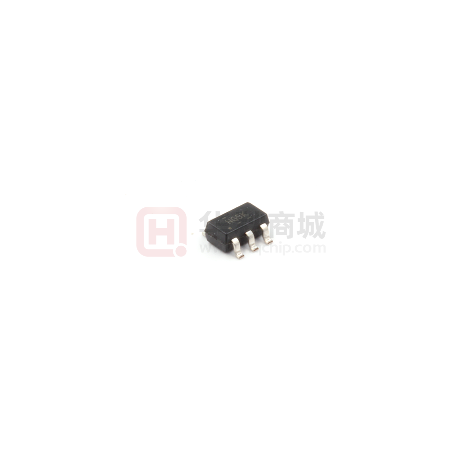
NG5K
(1)
The marketing status values are defined as follows:
ACTIVE: Product device recommended for new designs.
LIFEBUY: TI has announced that the device will be discontinued, and a lifetime-buy period is in effect.
NRND: Not recommended for new designs. Device is in production to support existing customers, but TI does not recommend using this part in a new design.
PREVIEW: Device has been announced but is not in production. Samples may or may not be available.
OBSOLETE: TI has discontinued the production of the device.
(2)
RoHS: TI defines "RoHS" to mean semiconductor products that are compliant with the current EU RoHS requirements for all 10 RoHS substances, including the requirement that RoHS substance
do not exceed 0.1% by weight in homogeneous materials. Where designed to be soldered at high temperatures, "RoHS" products are suitable for use in specified lead-free processes. TI may
reference these types of products as "Pb-Free".
RoHS Exempt: TI defines "RoHS Exempt" to mean products that contain lead but are compliant with EU RoHS pursuant to a specific EU RoHS exemption.
Green: TI defines "Green" to mean the content of Chlorine (Cl) and Bromine (Br) based flame retardants meet JS709B low halogen requirements of


 工商网监
湘ICP备2023018690号
工商网监
湘ICP备2023018690号

