Sample &
Buy
Product
Folder
Support &
Community
Tools &
Software
Technical
Documents
TPS61158
SLVSBR3A – MAY 2013 – REVISED JUNE 2015
TPS61158 30-V WLED Driver with Integrated Power Diode
1 Features
3 Description
•
•
•
With a 30V-rated integrated switch FET and power
diode, the TPS61158 is a boost converter that drives
LEDs in series. The boost converter runs at 750-kHz
fixed switching frequency to reduce output ripple,
improve conversion efficiency, and allows for the use
of small external components.
1
•
•
•
•
•
•
•
2.7-V to 5.5-V Input Voltage Range
28-V Open LED Protection (up to 8 LEDs)
Integrated 0.6-A, 30-V Internal Switch FET and
Power Diode
750-kHz Switching Frequency
Flexible Digital and PWM Brightness Control
– 1-Wire Control Interface (EasyScale™)
– PWM Dimming Control Interface
Up to 100:1 PWM Dimming Ratio
Integrated Loop Compensation
Built-in Soft Start
Built-in WLED Open protection
Thermal Shutdown
The default white LED current is set with the external
sensor resistor RFB, and the feedback voltage is
regulated to 200 mV, as shown in Typical Application.
During the operation, the LED current can be
controlled using the 1-wire digital interface
(EasyScale™ protocol) through the CTRL pin.
Alternatively, a pulse width modulation (PWM) signal
can be applied to the CTRL pin through which the
duty cycle determines the feedback reference
voltage. In either digital or PWM mode, the
TPS61158 does not burst the LED current; therefore,
it does not generate audible noises on the output
capacitor. For maximum protection, the device
features integrated open LED protection that disables
the TPS61158 to prevent the output voltage from
exceeding the device absolute maximum voltage
ratings during open LED conditions.
2 Applications
•
•
•
•
•
•
Feature Phones
Smart Phones
Portable Media Players
Ultra Mobile Devices
GPS Receivers
Backlight for Small and Media Form Factor LCD
Displays
Device Information(1)
PART NUMBER
TPS61158
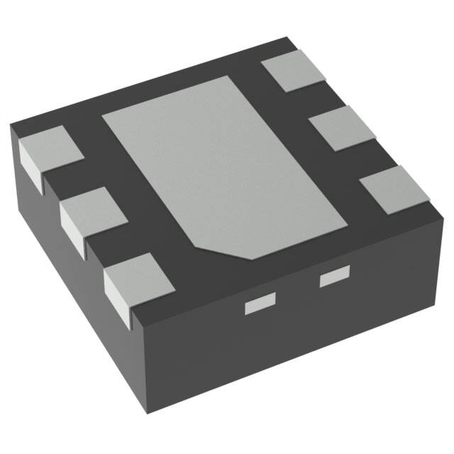
PACKAGE
WSON (6)
BODY SIZE (NOM)
2.00 mm x 2.00 mm
(1) For all available packages, see the orderable addendum at
the end of the data sheet.
space
Typical Application
L
10 to 22µH
2.7V ~ 5.5V
Up to 8 LEDs
VBAT
Cin
2.2µF
VIN
PWM or 1-wire
dimming control
Cout
1µF
TPS61158
LX
CTRL
VOUT
GND
FB
RFB
10
1
An IMPORTANT NOTICE at the end of this data sheet addresses availability, warranty, changes, use in safety-critical applications,
intellectual property matters and other important disclaimers. PRODUCTION DATA.
�TPS61158
SLVSBR3A – MAY 2013 – REVISED JUNE 2015
www.ti.com
Table of Contents
1
2
3
4
5
6
7
Features ..................................................................
Applications ...........................................................
Description .............................................................
Revision History.....................................................
Pin Configuration and Functions .........................
Specifications.........................................................
1
1
1
2
3
4
6.1
6.2
6.3
6.4
6.5
6.6
6.7
4
4
4
4
5
6
6
Absolute Maximum Ratings ......................................
ESD Ratings..............................................................
Recommended Operating Conditions.......................
Thermal Information ..................................................
Electrical Characteristics...........................................
EasyScale Timing Requirements..............................
Typical Characteristics ..............................................
Detailed Description .............................................. 8
7.1 Overview ................................................................... 8
7.2 Functional Block Diagram ......................................... 8
7.3 Feature Description................................................... 8
7.4 Device Functional Modes.......................................... 9
8
Application and Implementation ........................ 15
8.1 Application Information............................................ 15
8.2 Typical Application ................................................. 15
9 Power Supply Recommendations...................... 20
10 Layout................................................................... 21
10.1 Layout Guidelines ................................................. 21
10.2 Layout Example .................................................... 21
11 Device and Documentation Support ................. 22
11.1
11.2
11.3
11.4
11.5
Device Support......................................................
Community Resources..........................................
Trademarks ...........................................................
Electrostatic Discharge Caution ............................
Glossary ................................................................
22
22
22
22
22
12 Mechanical, Packaging, and Orderable
Information ........................................................... 22
4 Revision History
Changes from Original (May 2013) to Revision A
•
2
Page
Added Pin Configuration and Functions section, ESD Rating table, Feature Description, Device Functional Modes,
Application and Implementation, Power Supply Recommendations, Layout, Device and Documentation Support ,
and Mechanical, Packaging, and Orderable Information sections ......................................................................................... 1
Submit Documentation Feedback
Copyright © 2013–2015, Texas Instruments Incorporated
Product Folder Links: TPS61158
�TPS61158
www.ti.com
SLVSBR3A – MAY 2013 – REVISED JUNE 2015
5 Pin Configuration and Functions
DRV Package
6-Pin WSON
Top View
CTRL
1
VIN
2
VOUT
3
Thermal
pad
6
LX
5
GND
4
FB
Pin Functions
PIN
NO.
NAME
1
CTRL
I/O
DESCRIPTION
I
Control pin of the boost converter. It is a multi-functional pin which can be used for enable control,
PWM and digital dimming.
2
VIN
I
The input supply pin for the device. Connect VIN to a supply voltage between 2.7 V and 5.5 V.
3
VOUT
O
Output of the boost converter.
4
FB
I
Feedback pin for current. Connect the sense resistor from FB to GND.
5
GND
O
Ground
6
LX
I
This is the switching node of the device. Connect the inductor between the VIN and LX pin.
7
Thermal Pad
The thermal pad should be soldered to the analog ground plane. If possible, use thermal via to connect
to ground plane for ideal power dissipation.
Submit Documentation Feedback
Copyright © 2013–2015, Texas Instruments Incorporated
Product Folder Links: TPS61158
3
�TPS61158
SLVSBR3A – MAY 2013 – REVISED JUNE 2015
www.ti.com
6 Specifications
6.1 Absolute Maximum Ratings
over operating free-air temperature range (unless otherwise noted) (1)
MIN
MAX
UNIT
VIN
–0.3
6
V
VOUT, LX
–0.3
30
V
FB, CTRL
–0.3
7
V
Operating junction temperature
–40
150
°C
Storage temperature, Tstg
–65
150
°C
Voltage range
(2)
Continuous power dissipation
(1)
(2)
Stresses beyond those listed under Absolute Maximum Ratings may cause permanent damage to the device. These are stress ratings
only, which do not imply functional operation of the device at these or any other conditions beyond those indicated under Recommended
Operating Conditions. Exposure to absolute-maximum-rated conditions for extended periods may affect device reliability.
All voltage values are with respect to network ground terminal.
6.2 ESD Ratings
VALUE
V(ESD)
(1)
(2)
Electrostatic discharge
Human-body model (HBM), per ANSI/ESDA/JEDEC JS-001 (1)
±2000
Charged-device model (CDM), per JEDEC specification JESD22-C101 (2)
±500
UNIT
V
JEDEC document JEP155 states that 500-V HBM allows safe manufacturing with a standard ESD control process.
JEDEC document JEP157 states that 250-V CDM allows safe manufacturing with a standard ESD control process.
6.3 Recommended Operating Conditions
over operating free-air temperature range (unless otherwise noted)
MIN
NOM
MAX
UNIT
VIN
Input voltage
2.7
5.5
VOUT
Output voltage
VIN
29
V
V
IOUT
Output load current
30
mA
L
Inductor
10
22
µH
CI
Input capacitor
1
10
µF
CO
Output capacitor
0.47
2.2
µF
FPWM
Input PWM signal frequency
20
100
kHz
TA
Operating ambient temperature
–40
85
°C
TJ
Operating junction temperature
–40
125
°C
6.4 Thermal Information
TPS61158
THERMAL METRIC
(1)
DRV (WSON)
UNIT
6 PINS
RθJA
Junction-to-ambient thermal resistance
70.4
°C/W
RθJC(top)
Junction-to-case (top) thermal resistance
94.8
°C/W
RθJB
Junction-to-board thermal resistance
39.8
°C/W
ψJT
Junction-to-top characterization parameter
2.5
°C/W
ψJB
Junction-to-board characterization parameter
40.2
°C/W
RθJC(bot)
Junction-to-case (bottom) thermal resistance
10.2
°C/W
(1)
4
For more information about traditional and new thermal metrics, see the Semiconductor and IC Package Thermal Metrics application
report, SPRA953.
Submit Documentation Feedback
Copyright © 2013–2015, Texas Instruments Incorporated
Product Folder Links: TPS61158
�TPS61158
www.ti.com
SLVSBR3A – MAY 2013 – REVISED JUNE 2015
6.5 Electrical Characteristics
VIN = 3.6 V, CTRL = High, IFB current = 20 mA, IFB voltage = 200 mV, TA = –40°C to 85°C, typical values are at TA = 25°C
(unless otherwise noted).
PARAMETER
TEST CONDITIONS
MIN
TYP
MAX
VIN ramp down
2.2
2.35
VIN ramp up
2.5
2.65
UNIT
POWER SUPPLY
VIN
Input voltage range
VIN_UVLO
VIN undervoltage lockout threshold
VIN_HYS
VIN undervoltage lockout
hysteresis
IQ
Operating quiescent current into
VIN
ISD
Shutdown current
2.7
5.5
275
V
V
mV
Device enable, no switching and
no load (VFB = 0.4 V)
0.3
0.5
Device enable, switching 750 kHz
and no load (VFB = 0 V)
0.5
1.65
CTRL = GND
0.1
1
mA
µA
CONTROL LOGIC AND TIMING
VH
CTRL logic high voltage
VL
CTRL logic Low voltage
1.2
RPD
CTRL pin internal pull-down
resistor
VCTRL = 1.8 V
tSD
CTRL pulse width to shutdown
CTRL from high to low
3.5
194
V
0.4
300
V
kΩ
ms
VOLTAGE AND CURRENT REGULATION
VREF
Voltage feedback regulation
voltage
Duty = 100%
IFB
FB pin bias current
VFB = 200 mV
tREF
VREF filter time constant
200
206
mV
2
µA
230
µs
POWER SWITCH AND DIODE
RDS(ON)
N-channel MOSFET on-resistance
VIN = 3.6 V, TA = 25°C,
IOUT = 100 mA
VF
Power diode forward voltage
IDIODE = 0.2 A
ILEAK_LX
LX pin leakage current
VLX = 28 V
Ω
0.6
1
0.75
1
V
0.1
2
µA
600
750
900
kHz
88%
94%
0.5
0.6
0.7
A
OSCILLATOR
ƒSW
Oscillator frequency
Dmax
Maximum duty cycle of boost
switching
VFB = 0 V, measured on the drive
signal of the switch MOSFET
PROTECTION AND SOFT START
VIN = 3.6 V, D = DMAX
TA = 0°C to 85°C
ILIM
NMOS current limit
ILIM_Start
Start up current limit
tILIM_Start
Time step for start up current limit
VOVP
Open LED protection threshold
Tested at VOUT pin
VACKNL
Acknowledge output voltage low
Open drain, Rpullup = 15 kΩ to VIN
360
mA
8
27.5
28.2
ms
29
V
0.4
V
THERMAL SHUTDOWN
Tshutdown
Thermal shutdown threshold
160
°C
Thys
Thermal shutdown hysteresis
15
°C
Submit Documentation Feedback
Copyright © 2013–2015, Texas Instruments Incorporated
Product Folder Links: TPS61158
5
�TPS61158
SLVSBR3A – MAY 2013 – REVISED JUNE 2015
www.ti.com
6.6 EasyScale Timing Requirements
MIN
NOM
MAX
UNIT
tes_detect
EasyScale detection time (1), CTRL low
450
tes_delay
EasyScale detection delay
100
µs
tes_win
EasyScale detection window time, measured from CTRL high
3.5
ms
tstart
Start time of program stream
3.5
tEOS
End time of program stream
3.5
600
µs
tH_LB
High time of low bit, Logic 0
3.5
300
µs
tL_LB
Low time of low bit, Logic 0
2 × tH_LB
600
µs
tH_HB
High time of high bit, Logic 1
2 × tL_HB
600
µs
tL_HB
Low time of high bit, Logic 1
3.5
300
µs
3.5
µs
900
µs
µs
(2)
tvalACK
Acknowledge valid time (see
tACKN
Duration of acknowledge condition (see (2))
(1)
(2)
µs
)
To select EasyScale mode, the CTRL pin has to be low for more than tes_detect during tes_win
Acknowledge condition active 0, this condition will only be applied in case the RFA bit is set. Open drain output, line needs to be pulled
high by the host with resistor load.
6.7 Typical Characteristics
100
100
VIN = 3.6V
RFB = 10
90
Efficiency (%)
Efficiency (%)
90
80
70
60
6 LEDs
8 LEDs
50
20
70
60
6 LEDs (VOUT = 18.3V)
8 LEDs (VOUT = 24.4V
0
80
40
60
Dimming Duty Cycle (%)
80
50
0
100
Figure 1. Efficiency vs Dimming Duty Cycle
40
60
80
100
Figure 2. Efficiency vs Dimming Duty Cycle
0.7
80
70
60
VIN
= 3V
V
IN = 3 V
VIN
3.6V
V
V
IN ==3.6
V
V
VIN
4.2V
IN ==4.2
V
V
VIN
IN ==55V
8 LEDs (VOUT = 24.4V)
RFB = 10
50
0
20
40
60
80
100
Ilim - SwitchCurrent Limit (A)
90
Efficiency (%)
20
Dimming Duty Cycle (%)
100
0.65
0.6
0.55
VIN = 3.6V
0.5
-60
-40
-20
0
20
40
60
80
100
120
140
Temperature (oC)
Dimming Duty Cycle (%)
Figure 3. Efficiency vs Dimming Duty Cycle
6
VIN
V
V
IN ==33V
V
V
VIN
3.6V
IN ==3.6
V
V
VIN
4.2V
IN ==4.2
V
V
VIN
IN ==55V
6 LEDs (VOUT = 18.3V)
RFB = 10
Figure 4. Switch Current Limit vs Duty Cycle
Submit Documentation Feedback
Copyright © 2013–2015, Texas Instruments Incorporated
Product Folder Links: TPS61158
�TPS61158
www.ti.com
SLVSBR3A – MAY 2013 – REVISED JUNE 2015
1
200
0.9
180
0.8
160
VFB - FB Voltage (mV)
Ilim - Switch Current Limit (A)
Typical Characteristics (continued)
0.7
0.6
0.5
0.4
0.3
0.2
Temperature = 25oC
0.1
140
120
100
80
60
40
20
0
VFB (mV)
0
2.5
3
3.5
4
4.5
5
5.5
6
0
2
VIN - Input Voltage (V)
4
6
8 10 12 14 16 18 20 22 24 26 28 30 32
EasyScale Step
Figure 5. Switch Current Limit vs Temperature
Figure 6. FB Voltage vs EasyScale Step
VFB 200mV/div
VOUT 10V/div
ILED20mA/div
IL200mA/div
Figure 7. Open LED Protection
Submit Documentation Feedback
Copyright © 2013–2015, Texas Instruments Incorporated
Product Folder Links: TPS61158
7
�TPS61158
SLVSBR3A – MAY 2013 – REVISED JUNE 2015
www.ti.com
7 Detailed Description
7.1 Overview
The TPS61158 is a high efficiency boost converter with integrated power diode in a small package size. The
device is ideal for driving white LED in series. The serial LED connection provides even illumination by sourcing
the same output current through all LEDs, eliminating the need for expensive factory calibration. The device
integrates a 30-V, 0.6-A low-side switch MOSFET and a 30-V power diode, and operates in pulse width
modulation (PWM) with 750-kHz fixed switching frequency. For operation see the block diagram. The duty cycle
of the converter is set by the error amplifier output and the current signal applied to the PWM control comparator.
The control architecture is based on traditional current-mode control; therefore, slope compensation is added to
the current signal to allow stable operation for duty cycles larger than 50%. The feedback loop regulates the FB
pin to a low reference voltage (200 mV typical), reducing the power dissipation in the current sense resistor.
7.2 Functional Block Diagram
L
VBAT
Cin 10 to 22µH
2.2µF
LX
VIN
VOUT
UVLO
Cout
1µF
Gate driver
control
OVP
detection
VOVP
Ramp
Generator
OSC
+
Current
Sensor
Rsense
Comp
Soft
start-up
FB
Error
Amp
CTRL
VREF
RFB
10
PWM & EasyScale
Reference Control
GND
7.3 Feature Description
7.3.1 Soft Start-Up
Soft-start circuitry is integrated into the device to avoid a high inrush current during start-up. After the device is
enabled, the voltage at FB pin ramps up to the reference voltage in 32 steps with each step taking 341 μs. This
ensures that the output voltage rises slowly to reduce the input current. Additionally, during the start up process,
the current limit of the switch is set to half of the normal current limit specification. During this period, the input
current is kept below 360 mA (typical). See the start-up waveform of a typical example.
8
Submit Documentation Feedback
Copyright © 2013–2015, Texas Instruments Incorporated
Product Folder Links: TPS61158
�TPS61158
www.ti.com
SLVSBR3A – MAY 2013 – REVISED JUNE 2015
Feature Description (continued)
7.3.2 Shutdown
The TPS61158 enters shutdown mode when the CTRL voltage is logic low for more than 3.5 ms. During
shutdown, the input supply current for the device is less than 1 μA (maximum). Although the internal FET does
not switch in shutdown mode, there is still a DC current path between the input and the LEDs through the
inductor and the power diode. The minimum forward voltage of the LED array must exceed the maximum input
voltage to ensure that the LEDs remain off in shutdown. In the typical application with two or more LEDs, the
forward voltage is large enough to reverse bias the diode and keep leakage current low.
7.3.3 Current Program
The FB voltage is regulated by a low 0.2-V reference voltage. The LED current is programmed externally using a
current-sense resistor RFB in series with the LED string. The value of the RFB is calculated using Equation 1:
V
RFB = FB
ILED
where
•
•
•
•
RFB = current sense resistor at FB pin
VFB = 200 mV (regulated voltage of FB pin)
ILED = full-scale output current of LEDs
The output current tolerance depends on the FB voltage accuracy and the current sensor resistor accuracy. (1)
7.3.4 Undervoltage Lockout
An undervoltage lockout prevents operation of the device at input voltages below typical 2.2 V. When the input
voltage is below the undervoltage threshold, the device is shut down, and the internal switch FET is turned off. If
the input voltage rises by undervoltage lockout hysteresis, the device restarts.
7.3.5 Open LED Protection
Open LED protection circuitry prevents device damage as the result of white LED disconnection. The TPS61158
monitors the voltages at the VOUT pin and FB pin. The circuitry turns off the switch FET and shuts down the
device completely if both of the following two conditions are met: 1) the VOUT voltage reaches OVP threshold
(28.2 V typical); and 2) FB voltage is lower than half of its regulation voltage. This means the LED string is open
or the FB pin is short to ground. As a result, the output voltage falls to the level of the input supply. The device
remains in shutdown mode until it is enabled by pulling down the CTRL pin logic low for at least 3.5 ms and then
pulling it high.
7.3.6 Thermal Shutdown
An internal thermal shutdown turns off the device when the typical junction temperature of 160°C is exceeded.
The device is released from shutdown automatically when the junction temperature decreases by 15°C.
7.4 Device Functional Modes
7.4.1 LED Brightness Dimming Mode Selection
The CTRL pin is used for the control input for both dimming modes, PWM dimming and 1 wire dimming. The
dimming mode for the TPS61158 is selected each time the device is enabled. The default dimming mode is
PWM dimming. To enter the 1 wire mode, the following digital pattern on the CTRL pin must be recognized by
the device every time the device starts from the shutdown mode.
1. Pull CTRL pin high to enable the TPS61158 and to start the 1-wire detection window.
2. After the EasyScale detection delay (tes_delay, 100 μs) expires, drive CTRL low for more than the EasyScale
detection time (tes_detect, 450 μs).
3. The CTRL pin has to be low for more than EasyScale detection time before the EasyScale detection window
(tes_win, 3.5 ms) expires. EasyScale detection window starts from the first CTRL pin low-to-high transition.
Submit Documentation Feedback
Copyright © 2013–2015, Texas Instruments Incorporated
Product Folder Links: TPS61158
9
�TPS61158
SLVSBR3A – MAY 2013 – REVISED JUNE 2015
www.ti.com
Device Functional Modes (continued)
The device immediately enters the 1 wire mode once the above 3 conditions are met. The EasyScale
communication can start before the detection window expires. Once the dimming mode is programmed, it can
not be changed without another start up. This means the device needs to be shutdown by pulling the CTRL low
for 3.5 ms and restarts. See Figure 8 for a graphical explanation.
Insert battery
PWM signal
high
CTRL
low
PWM
mode
xxxxxxx
xxxxxxx
xxxxxxx
Startup
delay
FB ramp
Shutdown delay
200mV x duty cycle
FB
t
Insert battery
Enter ES mode
Programming
code
Enter ES mode
Timing window
Programming code
high
CTRL
low
ES detect time
ES
mode
Shutdown
xxxxxxx
xxxxxxxxx
FB ramp
delay
ES detect delay
FB ramp
Programmed value
(if not programmed, 200mV default )
Startup delay
FB
IC
Shutdown
50mV
Startup delay
xxx
50mV
Figure 8. Dimming Mode Detection and Soft Start
7.4.1.1 PWM Brightness Dimming
When the CTRL pin is constantly high, the FB voltage is regulated to 200 mV typically. However, the CTRL pin
allows a PWM signal to reduce this regulation voltage; therefore, it achieves LED brightness dimming. The
relationship between the duty cycle and FB voltage is given by Equation 2.
VFB = Duty × 200 mV
where
•
•
Duty = duty cycle of the PWM signal
200 mV = internal reference voltage
(2)
As shown in Figure 9, the device chops up the internal 200-mV reference voltage at the duty cycle of the PWM
signal. The pulse signal is then filtered by an internal low pass filter. The output of the filter is connected to the
error amplifier as the reference voltage for the FB pin regulation. Therefore, although a PWM signal is used for
brightness dimming, only the WLED DC current is modulated, which is often referred as analog dimming. This
eliminates the audible noise which often occurs when the LED current is pulsed in replica of the frequency and
duty cycle of PWM control. Unlike other scheme which filters the PWM signal for analog dimming, the TPS61158
regulation voltage is independent of the PWM logic voltage level which often has large variations.
For optimum performance, use the PWM dimming frequency in the range of 20 kHz to 100 kHz. Since the CTRL
pin is logic only pin, adding an external RC filter applied to the pin does not work.
10
Submit Documentation Feedback
Copyright © 2013–2015, Texas Instruments Incorporated
Product Folder Links: TPS61158
�TPS61158
www.ti.com
SLVSBR3A – MAY 2013 – REVISED JUNE 2015
Device Functional Modes (continued)
The minimum dimming duty cycle the device can support is 1% within the PWM dimming frequency range 20
kHz to 100 kHz.
VBG
200mV
CTRL
Error
Amplifer
EA output
FB
Figure 9. Block Diagram of Programmable FB Voltage Using PWM Signal
7.4.1.1.1 Digital 1-Wire Brightness Dimming
The CTRL pin features a simple digital interface to allow digital brightness control. The digital dimming can save
the processor power and battery life as it does not require a PWM signal all the time, and the processor can
enter idle mode if available.
The TPS61158 adopts the EasyScale™ protocol for the digital dimming, which can program the FB voltage to
any of the 32 steps with single command. The step increment increases with the voltage to produce pseudo
logarithmic curve for the brightness step. See the Table 1 for the FB pin voltage steps. The default step is full
scale when the device is first enabled (VFB = 200 mV). The programmed reference voltage is stored in an internal
register. A power reset clears the register value and reset it to default.
7.4.1.1.2 Easyscale: 1-Wire Digital Dimming
EasyScale is a simple but flexible one-pin interface to configure the FB voltage. The interface is based on a
master-slave structure, where the master is typically a microcontroller or application processor. Figure 10 and
Table 2 give an overview of the protocol. The protocol consists of a device specific address byte and a data byte.
The device specific address byte is fixed to 58 hex. The data byte consists of five bits for information, two
address bits ("00"), and the RFA bit. The RFA bit set to high indicates the Request for Acknowledge condition.
The Acknowledge condition is only applied if the protocol was received correctly. The advantage of EasyScale
compared with other one pin interfaces is that its bit detection is in a large extent independent from the bit
transmission rate. It can automatically detect bit rates between 1.1 kBit/sec and up to 100 kBit/sec.
Submit Documentation Feedback
Copyright © 2013–2015, Texas Instruments Incorporated
Product Folder Links: TPS61158
11
�TPS61158
SLVSBR3A – MAY 2013 – REVISED JUNE 2015
www.ti.com
Table 1. Selectable FB Voltage
FB
VOLTAGE
(mV)
D4
D3
D2
D1
D0
0
0
0
0
0
0
0
1
5
0
0
0
0
1
2
8
0
0
0
1
0
3
11
0
0
0
1
1
4
14
0
0
1
0
0
5
17
0
0
1
0
1
6
20
0
0
1
1
0
7
23
0
0
1
1
1
8
26
0
1
0
0
0
9
29
0
1
0
0
1
10
32
0
1
0
1
0
11
35
0
1
0
1
1
12
38
0
1
1
0
0
13
44
0
1
1
0
1
14
50
0
1
1
1
0
15
56
0
1
1
1
1
16
62
1
0
0
0
0
17
68
1
0
0
0
1
18
74
1
0
0
1
0
19
80
1
0
0
1
1
20
86
1
0
1
0
0
21
92
1
0
1
0
1
22
98
1
0
1
1
0
23
104
1
0
1
1
1
24
116
1
1
0
0
0
25
128
1
1
0
0
1
26
140
1
1
0
1
0
27
152
1
1
0
1
1
28
164
1
1
1
0
0
29
176
1
1
1
0
1
30
188
1
1
1
1
0
31
200
1
1
1
1
1
DATA IN
DATABYTE
Device Address
Start
Start DA7 DA6 DA5 DA4 DA3 DA2 DA1
0
1
0
1
1
0
0
DA0 EOS Start RFA
0
A1
A0
D4
D3
D2
D1
D0
EOS
DATA OUT ACK
Figure 10. EasyScale Protocol Overview
12
Submit Documentation Feedback
Copyright © 2013–2015, Texas Instruments Incorporated
Product Folder Links: TPS61158
�TPS61158
www.ti.com
SLVSBR3A – MAY 2013 – REVISED JUNE 2015
Table 2. EasyScale Bit Description
BYTE
BIT
NUMBER
NAME
7
DA7
0 (MSB device address)
6
DA6
1
5
DA5
0
4
DA4
3
DA3
2
DA2
0
1
DA1
0
0
DA0
0 (LSB device address)
7 (MSB)
RFA
Request for acknowledge. If high, acknowledge is applied by device.
6
A1
0 (Address bit A1)
5
A0
0 (Address bit A0)
4
D4
3
D3
2
D2
Data bit D2
1
D1
Data bit D1
0 (LSB)
D0
Data bit D0
Device
Address
Byte 72 hex
Data byte
TRANSMISSION
DIRECTION
1
IN
1
Data bit D4
IN
ACK
Data bit D3
Acknowledge condition active 0, this condition will only be applied to
case RFA bit is set. Open drain output, line needs to be pulled high
by the host with a pullup resistor. This feature can only be used if the
master has an open drain output stage. In case of a push pull output
stage Acknowledge condition may not be requested!
OUT
t Start
DATA IN
DESCRIPTION
t Start
Address Byte
DATA Byte
Static High
Static High
DA7
0
DA0
0
D0
1
RFA
0
TEOS
TEOS
Figure 11. EasyScale Timing, Without Acknowledge (RFA = 0)
t Start
DATA IN
t
Address Byte
Start
DATA Byte
Static High
Static High
DA7
0
DA0
0
TEOS
RFA
1
D0
1
Controller needs to
Pullup Data Line via a
resistor to detect ACKN
DATA OUT
t valACK
ACKN
t ACKN
Acknowledge
true, Data Line
pulled down by
device
Acknowledge
false, no pull
down
Figure 12. EasyScale Timing, With Acknowledge (RFA = 1)
Submit Documentation Feedback
Copyright © 2013–2015, Texas Instruments Incorporated
Product Folder Links: TPS61158
13
�TPS61158
SLVSBR3A – MAY 2013 – REVISED JUNE 2015
www.ti.com
tLow
Low Bit
(Logic 0)
tHigh
tLOW
tHigh
High Bit
(Logic 1)
Figure 13. EasyScale— Bit Coding
All bits are transmitted MSB first and LSB last. Figure 11 shows the protocol without acknowledge request (Bit
RFA = 0), Figure 12 with acknowledge (Bit RFA = 1) request. Prior to both bytes, device address byte and data
byte, a start condition must be applied. For this, the CTRL pin must be pulled high for at least tstart (3.5μs) before
the bit transmission starts with the falling edge. If the CTRL pin is already at high level, no start condition is
needed prior to the device address byte. The transmission of each byte is closed with an End of Stream
condition for at least tEOS (3.5μs).
The bit detection is based on a Logic Detection scheme, where the criterion is the relation between tLOW and
tHIGH (refer to Figure 13). It can be simplified to:
• Low Bit (Logic 0): tLOW ≥ 2 x tHIGH
• High Bit (Logic 1): tHIGH ≥ 2 x tLOW
The bit detection starts with a falling edge on the CTRL pin and ends with the next falling edge. Depending on
the relation between tHIGH and tLOW, the logic 0 or 1 is detected.
The acknowledge condition is only applied if:
• Acknowledge is requested by setting RFA bit to 1.
• The transmitted device address matches with the device address of the device.
• Device address byte and data byte are received correctly.
If above conditions are met, after tvalACK (3.5 μs) delay from the moment when the last falling edge of the protocol
is detected, an internal ACKN-MOSFET is turned on to pull the CTRL pin low for the time tACKN (900 μs
maximum), then the Acknowledge condition is valid. During the tvalACK delay, the master controller keeps the line
low; after the delay, it should release the line by outputting high impedance and then detect the acknowledge
condition. If it reads back a logic 0, it means the device has received the command correctly. The CTRL pin can
be used again by the master when the acknowledge condition ends after tACKN time.
Note that the acknowledge condition can only be requested in case the master device has an open drain output.
For a push-pull output stage, the use a series resistor in the CTRL line to limit the current to 500 μA is
recommended to for such cases as:
• an accidentally requested acknowledge, or
• to protect the internal ACKN-MOSFET.
14
Submit Documentation Feedback
Copyright © 2013–2015, Texas Instruments Incorporated
Product Folder Links: TPS61158
�TPS61158
www.ti.com
SLVSBR3A – MAY 2013 – REVISED JUNE 2015
8 Application and Implementation
NOTE
Information in the following applications sections is not part of the TI component
specification, and TI does not warrant its accuracy or completeness. TI’s customers are
responsible for determining suitability of components for their purposes. Customers should
validate and test their design implementation to confirm system functionality.
8.1 Application Information
The TPS61158 provides a high-performance LED lighting solution for mobile handsets and other low power LCD
backlit displays. The device can drive from 2 to 8 series LEDs in a compact and high efficient solution. An
internal rectifying diode eliminates the need for an external Schottky. The LED current is controlled via a logic
level PWM input with an internal low pass filter. This low pass filtered (analog) dimming, reduces the output
capacitor requirement and provides noise free current control.
8.2 Typical Application
L
10 to 22µH
2.7V ~ 5.5V
Up to 8 LEDs
VBAT
Cin
2.2µF
VIN
PWM or 1-wire
dimming control
Cout
1µF
TPS61158
LX
CTRL
VOUT
GND
FB
RFB
10
Figure 14. Typical Application for TPS61158
8.2.1 Design Requirements
For TPS61158 typical applications, use the parameters listed in Table 3 as the input parameters.
Table 3. Design Parameters
DESIGN PARAMETER
EXAMPLE VALUE
Minimum input voltage
2.7 V
Number of series LED
up to 8
Switching frequency
750 MHz
Submit Documentation Feedback
Copyright © 2013–2015, Texas Instruments Incorporated
Product Folder Links: TPS61158
15
�TPS61158
SLVSBR3A – MAY 2013 – REVISED JUNE 2015
www.ti.com
8.2.2 Detailed Design Procedure
8.2.2.1 Inductor Selection
The selection of the inductor affects steady state operation as well as transient behavior, loop stability and the
power conversion efficiency. These factors make it the most important component in power regulator design.
There are three important inductor specifications, inductor value, DC resistance, and saturation current.
Considering inductor value alone is not enough. The inductor value determines the inductor ripple current.
Choose an inductor that can handle the necessary peak current without saturating, according to half of the peakto-peak ripple current given by Equation 4, plus the inductor DC current given by:
V
´I
Iin _ DC = OUT OUT
VIN ´ h
(3)
Inductor values can have ±20% or even ±30% tolerance with no current bias. When the inductor current
approaches saturation level, its inductance can decrease 20% to 35% from the 0A value depending on how the
inductor vendor defines saturation. When selecting an inductor, please make sure its rated current, especially the
saturation current, is larger than its peak current during the operation. Using an inductor with a smaller
inductance value causes larger current ripple. This reduces the boost converter’s maximum output current,
causes large input voltage ripple and reduces efficiency. Large inductance value provides much more output
current and higher conversion efficiency. For these reasons, a 10-μH to 22-μH inductor value range is
recommended. A 22-μH inductor optimizes the efficiency for most application while maintaining low inductor
peak-to-peak ripple. Table 4 lists the recommended inductors for TPS61158. TPS61158 has built-in slope
compensation to avoid sub-harmonic oscillation associated with current mode control. If the inductor value is
lower than 10 μH, the slope compensation may not be adequate, and the loop can be unstable. Therefore,
customers need to verify the inductor in their application if it is different from the recommended values.
Table 4. Recommended Inductors
PART NUMBER
L (μH)
DCR MAX (mΩ)
SATURATION CURRENT
(A)
Size (L x W x H mm)
VENDOR
LPS3015-103ML
10
440
0.73
3.0 x 3.0 x 1.5
Coilcraft
LPS3015-223ML
22
825
0.5
3.0 x 3.0 x 1.5
Coilcraft
1229AS-H-100M
10
288
0.75
3.5 x 3.7 x 1.2
TOKO
1229AS-H-220M
22
672
0.5
3.5 x 3.7 x 1.2
TOKO
VLS3012ET-100M
10
336
0.64
3.0 x 3.0 x 1.2
TDK
VLS3012ET-220M
22
756
0.44
3.0 x 3.0 x 1.2
TDK
8.2.2.2 Maximum Output Current
The overcurrent limit in a boost converter limits the maximum input current and thus maximum input power for a
given input voltage. Maximum output power is less than maximum input power due to power conversion losses.
Therefore, the current limit setting, input voltage, output voltage and efficiency can all change maximum current
output. The current limit clamps the peak inductor current; therefore, the ripple has to be subtracted to derive
maximum DC current. The ripple current is a function of switching frequency, inductor value and duty cycle. The
following equations take into account of all the above factors for maximum output current calculation.
1
IP =
1
1
L ´ FS ´ (
)
+
VOUT + VF - VIN VIN
where
•
•
•
•
•
16
IP = inductor peak to peak ripple
L = inductor value
FS = switching frequency
VOUT = output voltage of the boost converter. It is equal to the sum of VFB and the voltage drop across LEDs.
VF = forward voltage of internal power diode. 0.75 V, typical
(4)
Submit Documentation Feedback
Copyright © 2013–2015, Texas Instruments Incorporated
Product Folder Links: TPS61158
�TPS61158
www.ti.com
SLVSBR3A – MAY 2013 – REVISED JUNE 2015
I OUT _ max =
VIN ´ (ILIM - IP / 2) ´ h
VOUT
where
•
•
•
IOUT_max = maximum output current of the boost converter
ILIM = overcurrent limit
η = boost efficiency (85%, typical)
(5)
To calculate the maximum output current in the worst case, use the minimum input voltage, maximum output
voltage and maximum forward voltage of internal power diode (1 V). In order to leave enough design margin, the
minimum current limit value 0.5 A, the minimum switching frequency 600 kHz, the inductor value with –30%
tolerance, and a low power conversion efficiency, such as 80% or lower are recommended for the calculation.
For instance, when minimum VIN is 3 V, 8 LEDs output equivalent to VOUT is 26 V, and the inductor is 22 µH,
then the maximum output current is 33 mA in the worst case.
8.2.2.3 Input and Output Capacitor Selection
The output capacitor is mainly selected to meet the requirements for the output ripple and loop stability. This
ripple voltage is related to the capacitor’s capacitance and its equivalent series resistance (ESR). Assuming a
capacitor with zero ESR, the minimum capacitance needed for a given ripple can be calculated by
- VIN ) ´ IOUT
(V
COUT = OUT
VOUT ´ FS ´ Vripple
where
•
Vripple = peak-to-peak output ripple.
(6)
The additional output ripple component caused by ESR is calculated using Equation 7:
Vripple_ESR = IOUT × RESR
(7)
Due to its low ESR, Vripple_ESR can be neglected for ceramic capacitors, but must be considered if tantalum or
electrolytic capacitors are used.
Care must be taken when evaluating a ceramic capacitor’s derating under DC bias, aging and AC signal. The DC
bias can significantly reduce capacitance. Ceramic capacitors can lose as much as 50% of its capacitance at its
rated voltage. Therefore, leave the margin on the voltage rating to ensure adequate capacitance at the required
output voltage.
The capacitor in the range of 1 μF to 10 μF is recommended for input side. The output requires a capacitor in the
range of 0.47 μF to 2.2 μF. The output capacitor affects the loop stability of the boost regulator. If the output
capacitor is below the range, the boost regulator can potentially become unstable.
The popular vendors for high value ceramic capacitors are:
TDK (http://www.component.tdk.com/components.php)
Murata (http://www.murata.com/cap/index.html)
Submit Documentation Feedback
Copyright © 2013–2015, Texas Instruments Incorporated
Product Folder Links: TPS61158
17
�TPS61158
SLVSBR3A – MAY 2013 – REVISED JUNE 2015
www.ti.com
8.2.3 Application Curves
250
DimmingDuty = 50% @ 20kHz
VFB - FB Voltage (mV)
CTRL 2V/div
200
150
VOUT (AC) 100mV/div
100
50
20kHz
ILED10mA/div
40kHz
0
0
20
40
60
80
100
Dimming Duty Cycle (%)
Figure 15. FB Voltage vs Dimming Duty Cycle
SW 20V/div
Figure 16. Output Ripple at PWM Dimming
SW 20V/div
VOUT (AC) 200mV/div
VOUT (AC) 50mV/div
IL100mA/div
IL100mA/div
Dimming Duty = 100%
Figure 17. Switching Waveform - Dimming Duty = 100%
Dimming Duty = 25%
Figure 18. Switching Waveform - Dimming Duty = 25%
CTRL 2V/div
CTRL 2V/div
VOUT 20V/div
VOUT 20V/div
ILED20mA/div
ILED5mA/div
IL200mA/div
IL100mA/div
Dimming Duty = 100%
Figure 19. Start-Up Dimming Duty = 100%
18
Submit Documentation Feedback
Dimming Duty = 25%
Figure 20. Start-Up Dimming Duty = 25%
Copyright © 2013–2015, Texas Instruments Incorporated
Product Folder Links: TPS61158
�TPS61158
www.ti.com
SLVSBR3A – MAY 2013 – REVISED JUNE 2015
CTRL 2V/div
CTRL 2V/div
VOUT 20V/div
VOUT 20V/div
ILED20mA/div
ILED5mA/div
IL200mA/div
IL100mA/div
Dimming Duty = 25%
Dimming Duty = 100%
Figure 21. Shutdown Dimming Duty = 100%
Figure 22. Shutdown Dimming Duty = 25%
8.2.4 Additional Application Circuits
8.2.4.1 TPS61158 To Drive Up To 8 LEDs
Figure 23 shows a typical application for the TPS61158. This can drive from 2 to 8 series WLEDs.
L
10 to 22µH
2.7V ~ 5.5V
Up to 8 LEDs
VBAT
Cin
2.2µF
VIN
PWM or 1-wire
dimming control
Cout
1µF
TPS61158
LX
CTRL
VOUT
GND
FB
RFB
10
Figure 23. TPS61158 to Drive up to 8 LEDs
8.2.4.2 TPS61158 to Drive up to 8 LEDs with RC Filter at VIN Pin
Figure 24 is typical application circuit with RC filter at IN.
Submit Documentation Feedback
Copyright © 2013–2015, Texas Instruments Incorporated
Product Folder Links: TPS61158
19
�TPS61158
SLVSBR3A – MAY 2013 – REVISED JUNE 2015
www.ti.com
L
10 to 22µH
2.7V ~ 5.5V
Up to 8 LEDs
VBAT
R1
10
Cin
2.2µF
VIN
C1
1µF
PWM or 1-wire
dimming control
Cout
1µF
TPS61158
LX
CTRL
VOUT
GND
FB
RFB
10
Figure 24. TPS61158 to Drive up to 8 LEDs With RC Filter at VIN Pin
9 Power Supply Recommendations
The TPS61158 requires a single supply input voltage. This voltage can range between 2.7 V to 5.5 V and must
be able to supply enough current for a given application.
20
Submit Documentation Feedback
Copyright © 2013–2015, Texas Instruments Incorporated
Product Folder Links: TPS61158
�TPS61158
www.ti.com
SLVSBR3A – MAY 2013 – REVISED JUNE 2015
10 Layout
10.1 Layout Guidelines
As for all switching power supplies, especially those high frequency and high current ones, layout is an important
design step. If layout is not carefully done, the regulator could suffer from instability as well as noise problems.
Therefore, use wide and short traces for high current paths. The input capacitor CIN needs to be close to the VIN
pin and GND pin in order to reduce the input ripple seen by the device. If possible, choose higher capacitance
value for it. If the ripple seen at VIN pin is so large that it affects the boost loop stability or internal circuits
operation, R1 and C1 is recommended to compose a filter to decouple the noise (refer to Figure 24). The SW pin
carries high current with fast rising and falling edges. Therefore, the connection between the SW pin to the
inductor should be kept as short and wide as possible. The output capacitor COUT should be put close to VOUT
pin. It is also beneficial to have the ground of COUT close to the GND pin since there is large ground return
current flowing between them. FB resistor should be put close to FB pin. When laying out signal grounds, it is
recommended to use short traces separated from power ground traces, and connect them together at a single
point close to the GND pin.
10.2 Layout Example
4.8 mm
LX
CTRL
IN
OUT
GND
6.5 mm
GND
FB
Figure 25. TPS61158 Example Layout
Submit Documentation Feedback
Copyright © 2013–2015, Texas Instruments Incorporated
Product Folder Links: TPS61158
21
�TPS61158
SLVSBR3A – MAY 2013 – REVISED JUNE 2015
www.ti.com
11 Device and Documentation Support
11.1 Device Support
11.1.1 Third-Party Products Disclaimer
TI'S PUBLICATION OF INFORMATION REGARDING THIRD-PARTY PRODUCTS OR SERVICES DOES NOT
CONSTITUTE AN ENDORSEMENT REGARDING THE SUITABILITY OF SUCH PRODUCTS OR SERVICES
OR A WARRANTY, REPRESENTATION OR ENDORSEMENT OF SUCH PRODUCTS OR SERVICES, EITHER
ALONE OR IN COMBINATION WITH ANY TI PRODUCT OR SERVICE.
11.2 Community Resources
The following links connect to TI community resources. Linked contents are provided "AS IS" by the respective
contributors. They do not constitute TI specifications and do not necessarily reflect TI's views; see TI's Terms of
Use.
TI E2E™ Online Community TI's Engineer-to-Engineer (E2E) Community. Created to foster collaboration
among engineers. At e2e.ti.com, you can ask questions, share knowledge, explore ideas and help
solve problems with fellow engineers.
Design Support TI's Design Support Quickly find helpful E2E forums along with design support tools and
contact information for technical support.
11.3 Trademarks
EasyScale, E2E are trademarks of Texas Instruments.
All other trademarks are the property of their respective owners.
11.4 Electrostatic Discharge Caution
These devices have limited built-in ESD protection. The leads should be shorted together or the device placed in conductive foam
during storage or handling to prevent electrostatic damage to the MOS gates.
11.5 Glossary
SLYZ022 — TI Glossary.
This glossary lists and explains terms, acronyms, and definitions.
12 Mechanical, Packaging, and Orderable Information
The following pages include mechanical, packaging, and orderable information. This information is the most
current data available for the designated devices. This data is subject to change without notice and revision of
this document. For browser-based versions of this data sheet, refer to the left-hand navigation.
22
Submit Documentation Feedback
Copyright © 2013–2015, Texas Instruments Incorporated
Product Folder Links: TPS61158
�PACKAGE OPTION ADDENDUM
www.ti.com
10-Dec-2020
PACKAGING INFORMATION
Orderable Device
Status
(1)
Package Type Package Pins Package
Drawing
Qty
Eco Plan
(2)
Lead finish/
Ball material
MSL Peak Temp
Op Temp (°C)
Device Marking
(3)
(4/5)
(6)
TPS61158DRVR
ACTIVE
WSON
DRV
6
3000
RoHS & Green
NIPDAU
Level-2-260C-1 YEAR
-40 to 85
SIW
(1)
The marketing status values are defined as follows:
ACTIVE: Product device recommended for new designs.
LIFEBUY: TI has announced that the device will be discontinued, and a lifetime-buy period is in effect.
NRND: Not recommended for new designs. Device is in production to support existing customers, but TI does not recommend using this part in a new design.
PREVIEW: Device has been announced but is not in production. Samples may or may not be available.
OBSOLETE: TI has discontinued the production of the device.
(2)
RoHS: TI defines "RoHS" to mean semiconductor products that are compliant with the current EU RoHS requirements for all 10 RoHS substances, including the requirement that RoHS substance
do not exceed 0.1% by weight in homogeneous materials. Where designed to be soldered at high temperatures, "RoHS" products are suitable for use in specified lead-free processes. TI may
reference these types of products as "Pb-Free".
RoHS Exempt: TI defines "RoHS Exempt" to mean products that contain lead but are compliant with EU RoHS pursuant to a specific EU RoHS exemption.
Green: TI defines "Green" to mean the content of Chlorine (Cl) and Bromine (Br) based flame retardants meet JS709B low halogen requirements of


 工商网监
湘ICP备2023018690号
工商网监
湘ICP备2023018690号


