TPS61185
www.ti.com
SLVSAA1A – APRIL 2010 – REVISED MAY 2010
WLED Driver for Notebooks with PWM Control Interface
Check for Samples: TPS61185
FEATURES
1
•
•
•
•
•
•
•
•
•
•
•
•
•
•
•
•
•
•
•
4.2 V to 24 V Input Voltage
Integrated 2 A/40 V MOSFET
600 kHz to 2 MHz Programmable Switching
Frequency
Adaptive Boost Output for Best Efficiency
Design to Use Small L-C Components
Integrated Loop Compensation
Eight 25 mA Current Sinks
Up to 10 WLED in Series
1% Current Matching and Accuracy
PWM Brightness Interface Control
200 mV Ripple Under PWM Dimming
Driver for Input/Output Isolation PFET
Programmable Over Voltage Threshold
100 Hz to 5 kHz Programmable PWM Dimming
Frequency
Up to 20 kHz Direct PWM Dimming Frequency
Enhanced Electrostatic Discharge Immunity
Level
Built-in WLED Open/Short Protection
Over Temperature Protection
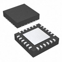
24 Pin 4 mm × 4 mm QFN Package
APPLICATIONS
•
The TPS61185 supports the PWM method for
brightness dimming. Simply tie the unused current
sinks to ground if fewer than eight are needed. During
PWM dimming, each of the eight current regulators is
turned on/off at the duty cycle determined by an
external pulse width modulation (PWM) signal input to
the PWM pin. The frequency at which each current
regulator turns on/off follows the input PWM signal on
the PWMIN pin if the MODE pin is grounded. If the
MODE pin is left floating or tied high, the regulators
turn on/off at the frequency programmed by an
external resistor on the FPWMO pin.
The TPS61185 IC supports boost switch frequency
programming from 600kHz to 2MHz by an external
resistor on the FSW pin. The device also provides a
driver output for an optional external PFET connected
between the input and inductor for truly disconnecting
the battery from LED during the shutdown or fault
protection.
The
device
integrates
resistor
programmable over-voltage protection, soft-start, and
thermal shutdown.
The TPS61185 IC has a built-in linear regulator to
power the internal circuits of the IC. The device is in a
4 mm × 4 mm QFN package.
Typical Application Circuit
L1
10 mH
4.2V~24V
C2
4.7 mF
C1
4.7 mF
FAULT
Notebook LCD Display Backlight
SW1
VIN
C4
1 mF
DESCRIPTION
The TPS61185 IC provides highly integrated
solutions for large-size LCD backlighting. This device
has a built-in high efficiency boost regulator with
integrated 2 A/40 V power MOSFET. The eight
current sink regulators provide high precision current
regulation and matching. In total, the device can
support up to 80 LEDs. In addition, the boost output
automatically adjusts its voltage to the WLED forward
voltage to improve efficiency.
D1
C3
1 mF
VDD
TPS61185
GND
R4
54.9 KW
OVP
FPWMO
EN
PWMIN
Open Freq Pro
SW2
PGND1
PGND2
R3
1 MW
R5
715 KW
MODE
Direct
R1
62 KW
IFB1
IFB2
IFB3
IFB4
IFB5
IFB6
IFB7
IFB8
ISET
FSW
AGND
R2
604 KW
1
Please be aware that an important notice concerning availability, standard warranty, and use in critical applications of Texas
Instruments semiconductor products and disclaimers thereto appears at the end of this data sheet.
PRODUCTION DATA information is current as of publication date.
Products conform to specifications per the terms of the Texas
Instruments standard warranty. Production processing does not
necessarily include testing of all parameters.
Copyright © 2010, Texas Instruments Incorporated
�TPS61185
SLVSAA1A – APRIL 2010 – REVISED MAY 2010
www.ti.com
PACKAGE INFORMATION (1)
(1)
PACKAGE
PACKAGE MARKING
TPS61185RGE
TPS61185
For the most current package and ordering information, see the
Package Option Addendum at the end of this document, or visit the
device product folder on ti.com.
ABSOLUTE MAXIMUM RATINGS (1)
over operating free-air temperature range (unless otherwise noted)
VALUE
Voltage range (2)
MAX
VIN and FAULT
–0.3
24
V
MODE
–0.3
7
V
SW
–0.3
40
V
EN, PWM, IFB1 to IFB8
–0.3
20
V
On all other pins
–0.3
3.6
V
See Thermal
Information Table
Continuous power dissipation
Temperature range
Operating junction, Tj
–40
150
°C
Storage, Tstg
–65
150
°C
Human Body Model (HBM)
ESD rating (3)
IFB1 to IFB8
5
On all other pins
2
Machine Model (MM)
Charge Device Model (CDM)
(1)
(2)
(3)
UNIT
MIN
kV
200
V
1
kV
Stresses beyond those listed under absolute maximum ratings may cause permanent damage to the device. These are stress ratings
only, and functional operation of the device at these or any other conditions beyond those indicated under recommended operating
conditions is not implied. Exposure to absolute-maximum-rated conditions for extended periods may affect device reliability.
All voltage values are with respect to network ground terminal.
ESD testing is performed according to the respective JESD22 JEDEC standard.
THERMAL INFORMATION
TPS61185
THERMAL METRIC (1)
RGE
UNITS
24
qJA
Junction-to-ambient thermal resistance (2)
qJC(top)
Junction-to-case(top) thermal resistance
qJB
Junction-to-board thermal resistance
yJT
Junction-to-top characterization parameter
yJB
Junction-to-board characterization parameter
qJC(bottom)
(1)
(2)
(3)
(4)
(5)
(6)
(7)
2
33.7
(3)
16.9
(4)
7.4
(5)
Junction-to-case(bottom) thermal resistance
0.5
(6)
(7)
°C/W
7.1
1.7
For more information about traditional and new thermal metrics, see the IC Package Thermal Metrics application report, SPRA953.
The junction-to-ambient thermal resistance under natural convection is obtained in a simulation on a JEDEC-standard, high-K board, as
specified in JESD51-7, in an environment described in JESD51-2a.
The junction-to-case (top) thermal resistance is obtained by simulating a cold plate test on the package top. No specific
JEDEC-standard test exists, but a close description can be found in the ANSI SEMI standard G30-88.
The junction-to-board thermal resistance is obtained by simulating in an environment with a ring cold plate fixture to control the PCB
temperature, as described in JESD51-8.
The junction-to-top characterization parameter, yJT, estimates the junction temperature of a device in a real system and is extracted
from the simulation data for obtaining qJA, using a procedure described in JESD51-2a (sections 6 and 7).
The junction-to-board characterization parameter, yJB, estimates the junction temperature of a device in a real system and is extracted
from the simulation data for obtaining qJA , using a procedure described in JESD51-2a (sections 6 and 7).
The junction-to-case (bottom) thermal resistance is obtained by simulating a cold plate test on the exposed (power) pad. No specific
JEDEC standard test exists, but a close description can be found in the ANSI SEMI standard G30-88.
Submit Documentation Feedback
Copyright © 2010, Texas Instruments Incorporated
Product Folder Link(s): TPS61185
�TPS61185
www.ti.com
SLVSAA1A – APRIL 2010 – REVISED MAY 2010
RECOMMENDED OPERATING CONDITIONS
MIN
NOM
MAX
UNIT
VBAT
Battery input voltage range
4.2
24
V
VOUT
Output voltage range
VIN
38
V
L
Inductor
4.7
10
µH
CI
Input capacitor
1.0
CO
Output capacitor
2.2
FPWMO
Internal, programmable PWM dimming frequency
FPWMIN
Input PWM Frequency
TON
Minimum on time in one dimming cycle
TA
Operating ambient temperature
–40
85
°C
TJ
Operating junction temperature
–40
125
°C
µF
10
µF
0.1
5
kHz
0.1
20
kHz
5
µs
ELECTRICAL CHARACTERISTICS
VIN = 10.8 V, EN = Logic High, IFB Current = 20 mA, IFB Voltage = 500 mV, TA = –40°C to 85°C, Typical Values are at TA =
25°C (unless otherwise noted)
PARAMETER
TEST CONDITIONS
MIN
TYP
MAX
UNIT
SUPPLY CURRENT
VIN
Battery input voltage range
Iq_VIN
Operating quiescent current into VIN
Device enable, VIN = 24 V,
No load, No switch
VDD
VDD pin output voltage
VIN > 5.5 V, ILoad = 3 mA
ISD
Shutdown current
Vin_UVLO
VIN under-voltage lockout threshold
Vin_hys
VIN under-voltage lockout hysterisis
4.2
24
V
0.5
3
mA
2.7
3.15
3.6
VIN = 10.8 V, EN = low
2
10
VIN = 21 V, EN = Low
4
15
VIN ramp down
3.7
VIN ramp up
3.8
100
3.9
4.1
4.2
150
V
µA
V
200
mV
EN, PWM and MODE
VH
EN logic high threshold
2.1
20
V
VL
EN logic Low threshold
0
0.8
V
VH
PWM logic high threshold
2.1
20
V
VL
PWM logic low threshold
VH
MODE logic high threshold
VL
MODE logic low threshold
RPD_EN
Pull down resistor on EN
VEN = 2.5 V
400
RPD_PWM
Pull down resistor on PWM
VPWM = 2.5 V
400
1.204
0
0.8
V
2.1
7
V
0
0.8
V
800
1600
kΩ
800
1600
kΩ
1.229
1.253
V
1.4%
mA
CURRENT REGULATION
VISET
ISET pin voltage
ISET current = 20 µA
KISET
Current multiple Iout/ISET
ISET current = 20 µA, D = 100%
IFB_AVG
Average current accuracy
ISET current = 20 µA, D = 100%
–1.4%
Km
(Imax-Imin)/IAVG
ISET current = 20 µA, D = 100%
0%
Ileak
IFB pin leakage current
IFB voltage = 20 V on all pins
IIFB_MAX
Current sink max output current
IFB = 500 mV
fdim
PWM dimming frequency
RFPWM = 715 kΩ
980
1%
0
3%
3
25
190
µA
mA
210
230
Hz
BOOST OUTPUT REGULATION
VIFB_L
VO dial up threshold
Measure on IFB
400
mV
VIFB_H
VO dial down threshold
Measure on IFB
900
mV
Vreg_L
0.72 ×
(1+R3/R4)
Min Vout regulation voltage
Submit Documentation Feedback
Copyright © 2010, Texas Instruments Incorporated
Product Folder Link(s): TPS61185
V
3
�TPS61185
SLVSAA1A – APRIL 2010 – REVISED MAY 2010
www.ti.com
ELECTRICAL CHARACTERISTICS (continued)
VIN = 10.8 V, EN = Logic High, IFB Current = 20 mA, IFB Voltage = 500 mV, TA = –40°C to 85°C, Typical Values are at TA =
25°C (unless otherwise noted)
PARAMETER
TEST CONDITIONS
MIN
TYP
MAX
UNIT
0.1
0.15
0.38
Ω
2
µA
POWER SWITCH
RPWM_SW
PWM FET on-resistance
ILN_NFET
PWM FET leakage current
VSW = 35 V, TA = 25°C
fS
Oscillator frequency
RFSW = 604 kΩ
Dmax
Maximum duty cycle
Dmin
Minimum duty cycle
0
OSCILLATOR
0.8
1.0
IFBx = 0 V, FSW = 600 kHz
89%
94%
FSW = 600 kHz
0.1%
1.2
MHz
7%
OC, SC, OVP AND SS
ILIM
N-channel MOSFET current limit
D = Dmax
3.1
A
VCLAMP_TH
VO clamp threshold
Measured on OVP pin
1.90
2
1.95
2.00
V
VOVP_TH
VO overvoltage threshold
Measured on OVP pin (rise)
1.97
2.03
2.09
V
Vovp_IFB
IFB overvoltage threshold
Measured on the IFBx pin, IFB on
4.4
4.8
5.2
V
Vovp2_IFB
2nd level IFB overvoltage threshold
Measured on the IFBx pin, IFB on and off
18
VIFB_nouse
IFB no use detection threshold during
start up
IFB voltage rising
IIFB_low
Low current detection threshold
As percentage of normal current
50%
VOL
OVP pin overload detection
Output voltage drop
60%
0.6
V
FAULT OUTPUT
Vfault_high
FAULT high voltage
Measured as VIN-VFAULT
Vfault_low
FAULT low voltage
Measured as VIN-VFAULT, Sink 10 µA,
VIN = 12 V
Ifault
FAULT pull-down current
VIN = 12 V
0.03
0.07
0.13
V
6
8
10
V
10
20
30
µA
THERMAL SHUTDOWN
Tshutdown
4
Thermal shutdown threshold
170
Submit Documentation Feedback
°C
Copyright © 2010, Texas Instruments Incorporated
Product Folder Link(s): TPS61185
�TPS61185
www.ti.com
SLVSAA1A – APRIL 2010 – REVISED MAY 2010
DEVICE INFORMATION
VDD
VIN
MODE
FAULT
SW1
SW2
24 PIN RGE PACKAGE
TOP VIEW
24
23
22
21
20
19
EN 1
18 PGND 1
FSW 2
17 PGND 2
16 OVP
FPWMO 3
TPS61185
13 IFB3
IFB8
7
8
9
10
11
12
IFB4
PWMIN 6
ISET
14 IFB2
IFB5
GND 5
IFB6
15 IFB1
IFB7
NC 4
PIN FUNCTIONS
PIN
NAME
NO.
I/O
DESCRIPTION
EN
1
I
Device enable pin.
FSW
2
I
Switching frequency program pin. Use a resistor from this pin to GND to set the boost switch frequency
from 600 kHz to 2 MHz.
FPWMO
3
O
Dimming frequency program pin. When the mode pin is open or pulled high, the resistor on this pin to GND
programs the PWM dimming frequency between 100 Hz to 5 kHz.
NC
4
I
No connection pin.
GND
5
I
Signal ground of the IC. Tie the ground of noise sensitive components to GND.
PWMIN
6
I
Dimming control logic input. The dimming frequency range is 100 Hz to 20 kHz.
7–10
12–15
O
Current sink regulation inputs. They are connected to the cathode of the WLEDs. Connect any unused IFB
pins to GND or leave open. The PWM loop regulates the lowest VIFB to 400 mV. Each channel is limited to
25 mA current.
ISET
11
O
The resistor on this pin programs WLED output current. Tie resistor ground to GND.
OVP
16
I
Over voltage programming pin. The OVP voltage threshold is set through an external resistor divider
combination according to equation 4.
PGND2
17
I
PGND1
18
I
Power grounds of the IC. Internally connect to the source of the PWM switch. Tie the ground of power
stage components to these grounds.
SW2
19
I
SW1
20
I
FAULT
21
O
Gate driver output for an external PFET used for fault protection. It can also be used as signal output for
system fault report.
MODE
22
I
Dimming mode select pin. When MODE is high or open, the internal dimming frequency is programmable
by a resistor on pin 3 (FPWMO pin); when MODE is low, the internal dimming frequency is the same as the
PWM input signal on pin 6 (PWMIN pin).
VIN
23
I
This pin is connected to the battery supply. It also provides the pull-up voltage for the FAULT pin.
VDD
24
O
The supply rail of internal logic. Connect a 1-µF capacitor from VDD to GND.
IFB8-IFB5
IFB4-IFB1
Drain connections of the internal PWM switch MOSFET and external Schottky diode.
Submit Documentation Feedback
Copyright © 2010, Texas Instruments Incorporated
Product Folder Link(s): TPS61185
5
�TPS61185
SLVSAA1A – APRIL 2010 – REVISED MAY 2010
www.ti.com
TYPICAL CHARACTERISTICS
TABLE OF GRAPHS
FIGURES
Load efficiency of TPS61185
VIN = 10.8 V; VO = 29 V, 31 V, 33 V and 36 V; L = 10 µH
Figure 1
Load efficiency of TPS61185
VIN = 7 V, 10.8 V and 24 V; VO = 31 V; L = 10 µH
Figure 2
PWM dimming efficiency
VIN = 7 V, 10.8 V and 24 V; VO = 36 V; L = 10 µH; RISET = 62 kΩ
Figure 3
PWM dimming efficiency
VIN = 7 V, 10.8 V and 24 V; VO = 30 V; L = 10 µH; RISET = 62 kΩ
Figure 4
Dimming linearity
VIN = 10.8 V; VO = 36 V; FPWMO = 210 Hz; RISET = 62 kΩ; MODE = OPEN
Figure 5
Dimming linearity
VIN = 10.8 V; VO = 36 V; FPWMO = 1 kHz; RISET = 62 kΩ; MODE = OPEN
Figure 6
Dimming linearity
VIN = 10.8 V; VO = 36 V; FPWMO = 210 Hz; RISET = 62 kΩ; MODE = GND
Figure 7
Dimming linearity
VIN = 10.8 V; VO = 36 V; FPWMO = 20 kHz; RISET = 62 kΩ; MODE = GND
Figure 8
Boost switching frequency
VIN = 10.8 V; VO = 36 V; RISET = 62 kΩ; MODE = OPEN
Figure 9
Programmable PWM dimming frequency
VIN = 10.8 V; VO = 36 V; RISET = 62 kΩ; MODE = OPEN
Figure 10
Switching waveform
VIN = 5 V; VO = 36 V; L = 10 µH; RISET = 62 kΩ
Figure 11
Switching waveform
VIN = 21 V; VO = 36 V; L = 10 µH; RISET = 62kΩ
Figure 12
Startup waveform
VIN = 10.8 V; VO = 36 V; RISET = 62 kΩ
Figure 13
Shutdown waveform
VIN = 10.8 V; VO = 36 V; RISET = 62kΩ
Figure 13
PWM dimming
VIN = 10.8 V; VO = 36 V; ISET = 20 µA; FPWMO = 210 Hz; D = 1%
Figure 15
PWM dimming
VIN = 10.8 V; VO = 36 V; ISET = 20 µA; FPWMO = 20 kHz; D = 10%
Figure 16
100
100
VI = 10.8 V
98
98
VO = 31 V
VO = 29 V
VO = 31 V
96
96
94
Efficiency - %
Efficiency - %
94
92
VO = 36 V
90
VO = 33 V
92
90
VI = 7 V
88
88
86
86
84
84
82
0
50
100
150
200
IO - Output Current - mA
250
300
82
0
Figure 1. Efficiency vs. Output Current
6
VI = 24 V
VI = 10.8 V
Submit Documentation Feedback
50
100
150
200
IO - Output Current - mA
250
300
Figure 2. Efficiency vs. Output Current
Copyright © 2010, Texas Instruments Incorporated
Product Folder Link(s): TPS61185
�TPS61185
www.ti.com
100
SLVSAA1A – APRIL 2010 – REVISED MAY 2010
100
VO = 36 V
VO = 30 V
90
90
80
80
VI = 7 V
70
Efficiency - %
Efficiency - %
VI = 7 V
VI = 24 V
VI = 10.8 V
60
50
70
60
50
40
40
30
30
20
0
20
40
60
PWM - %
80
20
0
100
VI = 24 V
VI = 10.8 V
Figure 3. Efficiency vs. PWM Dimming %
20
40
60
PWM - %
80
100
Figure 4. Efficiency vs. PWM Dimming %
160
160
FPWMO = 210 Hz
140
FPWMO = 1 KHz
VI = 7 V
140
VI = 7 V
VI = 10.8 V
IO - Output Current - mA
IO - Output Current - mA
VI = 10.8 V
120
100
80
VI = 24 V
60
40
100
VI = 24 V
80
60
40
20
20
0
0
120
20
40
60
PWM Duty Cycle - %
80
Figure 5. Output Current vs. PWM Duty Cycle
100
0
0
20
40
60
PWM Duty Cycle - %
80
100
Figure 6. Output Current vs. PWM Duty Cycle
Submit Documentation Feedback
Copyright © 2010, Texas Instruments Incorporated
Product Folder Link(s): TPS61185
7
�TPS61185
SLVSAA1A – APRIL 2010 – REVISED MAY 2010
www.ti.com
160
160
FPWMO = 210 Hz
VI = 7 V
FPWMO = 20 KHz
VI = 10.8 V
120
100
80
VI = 24 V
60
40
20
0
0
VI = 10.8 V
120
100
VI = 24 V
80
60
40
20
20
40
60
PWM Duty Cycle - %
80
0
0
100
Figure 7. Output Current vs. PWM Duty Cycle
20
40
60
PWM Duty Cycle - %
80
100
Figure 8. Output Current vs. PWM Duty Cycle
2000
5000
VI = 10.8 V
1900
VI = 10.8 V
4500
Brightness Dimming Frequency - Hz
1800
Boost Switch Frequency - KHz
VI = 7 V
140
IO - Output Current - mA
IO - Output Current - mA
140
1700
1600
1500
1400
1300
1200
1100
1000
900
800
4000
3500
3000
2500
2000
1500
1000
500
700
600
300
400
500
600
700
800
900
1000
0
0
RFSW - kW
Figure 9. Boost Switch Frequency vs. RFSW
8
200
400
600
RFPWMO - kW
800
1000
Figure 10. Brightness Dimming Frequency vs. RFPWMO
Submit Documentation Feedback
Copyright © 2010, Texas Instruments Incorporated
Product Folder Link(s): TPS61185
�TPS61185
www.ti.com
SLVSAA1A – APRIL 2010 – REVISED MAY 2010
VO
100 mV/div
AC
VO
100 mV/div
AC
SW
20 V/div
DC
SW
20 V/div
DC
Inductor
Current
1 A/div
DC
Inductor
Current
500 mA/div
DC
t - Time - 1 ms/div
t - Time - 1 ms/div
Figure 11. Switching Waveform
Figure 12. Switching Waveform
VO
10 mV/div
DC
VO
10 mV/div
DC
EN
2 V/div
DC
EN
2 V/div
DC
IFB1
5 V/div
DC
IFB1
5 V/div
DC
Inductor
Current
1 A/div
DC
Inductor
Current
1 A/div
DC
t - Time - 40 ms/div
t - Time - 40 ms/div
Figure 13. Startup Waveform
Figure 14. Shutdown Waveform
Submit Documentation Feedback
Copyright © 2010, Texas Instruments Incorporated
Product Folder Link(s): TPS61185
9
�TPS61185
SLVSAA1A – APRIL 2010 – REVISED MAY 2010
www.ti.com
VO
200 mV/div
DC
VO
200 mV/div
DC
IFB1
10 V/div
DC
IFB1
10 V/div
DC
Inductor
Current
1 A/div
DC
Inductor
Current
1 A/div
DC
t - Time - 2 ms/div
t - Time - 20 ms/div
Figure 15. Dimming Waveform
10
Submit Documentation Feedback
Figure 16. Dimming Waveform
Copyright © 2010, Texas Instruments Incorporated
Product Folder Link(s): TPS61185
�TPS61185
www.ti.com
SLVSAA1A – APRIL 2010 – REVISED MAY 2010
FUNCTIONAL BLOCK DIAGRAM
L
Diode
VIN
FAULT
C2
4.7 mF
SW1,2
C1
4.7 mF
OUTPUT
R3
OVP Protection
R
Q
OVP
S
VIN
VDD
Slope
Compensation
PGND
1,2
S
R4
Linear
Regulator
C3
1 mF
Ref
Comp
Error
Amp
IFB detect
circuit
FSW
Oscillator
R2
IFB1
ISET
Current Mirror
Current REF
EA
R1
EN
FPWMO
PWM Signal
Generator
Duty cycle
counter
M
U
X
Dimming
Control
R5
PWMIN
MODE
EN
Shutdown
Current Sink
AGND
Current Sink
IFB2
Current Sink
IFB3
Current Sink
IFB4
Current Sink
IFB5
Current Sink
IFB6
Current Sink
IFB7
Current Sink
IFB8
Submit Documentation Feedback
Copyright © 2010, Texas Instruments Incorporated
Product Folder Link(s): TPS61185
11
�TPS61185
SLVSAA1A – APRIL 2010 – REVISED MAY 2010
www.ti.com
DETAILED DESCRIPTION
NORMAL OPERATION
The TPS61185 is a high efficiency, high output voltage white LED driver for notebook panel backlighting
applications. The advantages of white LEDs compared to CCFL backlights are higher power efficiency and lower
profile design. Due to the large number of white LEDs required to provide backlighting for medium to large
display panels, the LEDs must be arranged in parallel strings of several LEDs in series. Therefore, the backlight
driver for battery powered systems is almost always a boost regulator with multiple current sink regulators.
Having more white LEDs in series reduces the number of parallel strings and therefore improves overall current
matching. However, the efficiency of the boost regulator declines due to the need for high output voltage. Also,
there must be enough white LEDs in series to ensure the output voltage stays above the input voltage range.
The TPS61185 IC has integrated all of the key functional blocks to power and control up to 80 white LEDs. The
device includes a 2 A/40 V boost regulator, eight 25 mA current sink regulators, and protection circuitry for
over-current, over-voltage, and short circuit failures.
The TPS61185 provides a PMW interface to control the current of each regulator to realize the LED brightness
dimming.
SUPPLY VOLTAGE
The TPS61185 IC has a built-in LDO linear regulator to supply the IC analog and logic circuit. The LDO is
powered up when the EN pin is high. The output of the LDO is connected to the VDD pin. A 1 µF bypass
capacitor on the VDD pin is required for the LDO control loop to be stable. While possible to enable the IC by
tying EN to the VDD for evaluation purposes, it is recommended to use a separate digital signal to enable and
disable the IC in a real system.
The voltage on the VIN pin is the input of the internal LDO and powers the IC. There is an under-voltage lockout
on the VIN pin which disables the IC when its voltage falls to 4.0 V (maximum). The IC restarts when the VIN pin
voltage recovers by 200 mV.
BOOST REGULATOR AND PROGRAMMABLE SWITCH FREQUENCY (FSW)
The fixed-frequency PWM boost converter uses current-mode control and has integrated loop compensation.
The internal compensation ensures stable output over the full input and output voltage ranges assuming the
recommended values of inductor and output capacitor on page 3 are used. The output voltage of the boost
regulator is automatically set by the IC to minimize the voltage drop across the IFB pins. The IC regulates the
lowest IFB pin to 400 mV and consistently adjusts the boost output voltage to account for any changes in LED
forward voltages. If the input voltage is higher than the sum of the white LED forward voltage drops (e.g., at low
duty cycles), the boost converter is not able to regulate the output due to its minimum duty cycle limitation. In this
case, increase the number of LEDs in series or include series ballast resistors in order to provide enough
headroom for the converter to boost the output voltage. Since the TPS61185 integrates a 2 A/40 V power
MOSFET, the boost converter can provide up to a 38 V output voltage.
The TPS61185 switch frequency is programmable between 600 kHz to 2.0MHz by the resistor value on the FSW
pin and approximately follows Equation 1:
FSW »
6 ´ 1011
RFSW
(1)
Where: RFSW = FSW pin resistor
See Figure 9 for boost converter switching frequency adjustment resistor RFSW selection.
The adjustable switching frequency feature provides the user with the flexibility of choosing a faster switching
frequency, and therefore, an inductor with smaller inductance and footprint, or a slower switching frequency, and
therefore, potentially higher efficiency due to lower switching losses.
12
Submit Documentation Feedback
Copyright © 2010, Texas Instruments Incorporated
Product Folder Link(s): TPS61185
�TPS61185
www.ti.com
SLVSAA1A – APRIL 2010 – REVISED MAY 2010
LED CURRENT SINKS
The eight current sink regulators embedded in the TPS61185 can be collectively configured to provide up to a
maximum of 25 mA. These eight specialized current sinks are accurate to within ±1% typical maximum for
currents above 5 mA, with a string-to-string difference of ±1% . The IFB current must be programmed to the
highest LED current expected using the ISET pin resistor and Equation 2.
V
IFB = ISET ´ K ISET
RISET
(2)
Where:
KISET = Current multiple (980 typical)
VISET = ISET pin voltage (1.229 V typical)
RISET = ISET pin resistor
ENABLE AND SOFT STARTUP
A logic high signal on the EN pin turns on the internal LDO linear regulator which provides VDD to activate the
IC. After the device is enabled, the TPS61185 checks the status of all current feedback channels and shuts down
any unused feedback channels.
After the device is enabled, if the PWMIN pin is left floating or logic low input, the output voltage of the
TPS61185 regulates to the minimum output voltage. Once the IC detects a voltage on the PWMIN pin, the
TPS61185 begins to regulate the IFB pin current, as pre-set per the ISET pin resistor, times the duty cycle of the
signal on the PWMIN pin. The boost converter’s output voltage rises to the appropriate level to accommodate the
sum of the white LED string with the highest forward voltage drop plus 400 mV typical at that current.
The TPS61185 has integrated soft-start circuitry to avoid any inrush current during startup. During the startup
period, the TPS61185 output voltage rises step by step from the minimum output voltage in 100 mV increments,
over a 1 ms interval. After startup, the output voltage continues to rise until all of the IFB pin voltages exceed 400
mV and all IFB current is regulated under the pre-set value.
Pulling the EN pin low immediately shuts down the IC, resulting in the IC consuming less than 50 µA in shutdown
mode.
IFB PIN UNUSED
If the application requires less than 8 WLED strings, those IFB pins not required can be easily disabled. The
TPS61185 simply requires leaving the unused IFB pin open or shorting it to ground. If the IFB pin is open, the
boost output voltage ramps up to the pre-set over-voltage threshold on the VOVP pin during start up. The IC then
detects the zero current string and removes it from the feedback loop. If the IFB pin is shorted to ground, the IC
detects the voltage less than the VIFB_nouse threshold typically 0.6V and immediately disables the string after the
IC is enabled. Thus, the boost output voltage ramps to the regulation voltage immediately following soft start and
does not go up to the over-voltage threshold.
BRIGHTNESS DIMMING (MODE)
The TPS61185 adopts PWM dimming technology for output LED brightness control. All output current strings are
turned on and off together at the duty cycle which is determined by the PWM signal input to the PWMIN pin.
However, the TPS61185 has two PWM dimming methods to control LED brightness. The voltage level of the
MODE pin determines the PWM dimming method. Direct PWM dimming mode is selected with the MODE pin
tied to GND. The frequency programmable dimming mode is selected by either leaving the MODE pin open or
pulling it high to VDD. In direct PWM dimming mode, the dimming frequency is synchronized to the PWM signal
input on the PWMIN pin, while in frequency programmable dimming mode, the internal PWM dimming frequency
is set by the resistor on the FPWMO pin.
DIRECT PWM DIMMING
In direct PWM dimming mode, all used IFB channels turn on and off together at the same frequency and duty
cycle as the input PWM on the PWMIN pin. Figure 17 shows the timing diagram for direct PWM dimming.
Submit Documentation Feedback
Copyright © 2010, Texas Instruments Incorporated
Product Folder Link(s): TPS61185
13
�TPS61185
SLVSAA1A – APRIL 2010 – REVISED MAY 2010
www.ti.com
D = 35%
D = 50%
PWM
D = 10%
TON
TPWM
I LED
IFB 1
IFB 2
IFB 3
IFB 8
Figure 17. Direct PWM Dimming Timing Diagram
FREQUENCY PROGRAM PWM DIMMING
In this mode, all used IFB channels are turned on and off together at the internal oscillator frequency as set by
the resistor on the FPWMO pin. Figure 18 shows the timing diagram for each channel when running in frequency
program PWM dimming mode.
PWM
D = 35%
TON
TPWM
I LED
TDIM
IFB 1
D = 35%
IFB 2
IFB 3
IFB 8
Figure 18. Frequency Program PWM Dimming Timing Diagram
The built-in oscillator is adjustable by an external resistor RFPWMO on the FPWMO pin and is in the range of 100
Hz to 5 kHz approximately following Equation 3:
FPW MO »
1.5 ´ 108
RFPWMO
(3)
Where: RFPWMO = FPWMO pin resistor
14
Submit Documentation Feedback
Copyright © 2010, Texas Instruments Incorporated
Product Folder Link(s): TPS61185
�TPS61185
www.ti.com
SLVSAA1A – APRIL 2010 – REVISED MAY 2010
The adjustable range of the RFPWMO resistor is from 27 kΩ to 1.5 MΩ, corresponding to the dimming frequency,
FPWMO, of 100 Hz to 5 kHz. See Figure 10 for PWM dimming frequency adjustment resistor RFPWMO selection and
Table 1 for the resistor value recommendation list.
Table 1. Resistor Value Recommendation List
RFPWMO
FPWMO
715 kΩ
210 Hz
309 kΩ
500 Hz
150 kΩ
1000 Hz
72.3 kΩ
2000 Hz
During PWM dimming, minimum on time in each dimming cycle is 5 µs typical. This means the minimum duty
cycle of PWM dimming can be down to 1% when the dimming frequency is less than 2 kHz.
OVER VOLTAGE PROTECTION (OVP)
The TPS61185 has two levels of protection to prevent the output, and therefore the SW pins, from exceeding a
certain voltage. The output voltage clamp circuit limits the output voltage to the user selected value by limiting
the internal feedback loop reference level. The clamp circuit response time is not fast enough to protect against
output voltage transients or high-voltage noise spikes that couple from external circuits. So, if the over voltage
(OV) circuit detects the output going 80 mV higher than the clamp voltage, it turns off the boost switch until the
output voltage drops below the clamp voltage. Resistors R3 and R4 in Typical Application Circuit set the output
voltage clamp threshold and OV threshold as computed by Equation 4 and Equation 5.
R3 ö
æ
VO UT_CLAMP = VCLAMP_TH ´ ç 1 +
÷
R4 ø
è
(4)
R3 ö
æ
VOUT_OV = VOV_TH ´ ç 1 +
÷
R4 ø
è
(5)
Where:
VCLAMP_TH = 1.95 V typically
VOV_TH = 2.03 V typically
In the Typical Application Circuit, the output OVP voltage is set to:
1M ö
æ
VOUT_CLAMP = 1.95 ´ ç 1 +
÷ = 37.5 V
54.9 K ø
è
(6)
1M ö
æ
VO UT_OV = 2.03 ´ ç 1 +
÷ = 39.0 V
54.9K ø
è
(7)
CURRENT SINK OPEN AND SHORT PROTECTION
For the TPS61185, if one of the WLED strings is open, the boost output rises to the output voltage clamp
threshold. The IC detects the open WLED string by sensing no current on the corresponding IFB pin. As a result,
the IC deactivates the open IFB pin and removes it from the voltage feedback loop. Subsequently, the output
voltage returns to the minimum voltage required for the connected WLED strings. The IFB pin currents of the
connected WLED strings remain in regulation during this process.
If any IFB pin voltage exceeds the IFB over voltage threshold (5 V typical), the IC turns off the corresponding
current sink and removes this IFB pin from the output voltage regulation loop. Current regulation of the remaining
IFB pins is not affected. This condition often occurs when there are several shorted WLEDs in one string. WLED
mismatch typically does not create such a large voltage difference among WLED strings.
The IC only shuts down if it detects that all of the WLED strings are open. If any open WLED string is
reconnected, it is reactivated automatically.
Submit Documentation Feedback
Copyright © 2010, Texas Instruments Incorporated
Product Folder Link(s): TPS61185
15
�TPS61185
SLVSAA1A – APRIL 2010 – REVISED MAY 2010
www.ti.com
OVER CURRENT AND SHORT CIRCUIT PROTECTION
The TPS61185 pulse by pulse over-current limit is 2.0 A (min). The PWM switch turns off when the inductor
current reaches this current threshold. The PWM switch remains off until the beginning of the next switching
cycle. This protects the IC and external components under over-load conditions. When there is a sustained
over-current condition, the IC turns off and requires a POR or EN pin toggling to restart.
Under severe over-load and/or short circuit conditions, the boost output voltage can be pulled below the required
regulated voltage to keep all of the white LEDs operating with all IFB voltage higher than 400 mV. Under this
condition, the current flows directly from input to output through the inductor and schottky diode. To protect the
TPS61185, the device shuts down immediately. The IC restarts after input POR or EN pin logic toggling.
SKIP PULSE OPERATION
When the input voltage on the VIN pin is less than 1 V higher than the total LED forward voltage, the TPS61185
boost regulator operates in skip pulse mode. In pulse skip mode, the main switch turns on/off for several cycles
to charge the inductor and output capacitor and continues to regulate the output voltage and current sinks
continue to regulate the IFB pin current.
If the input voltage is more than 1 V higher than the output total LED forward voltage, the boost regulator shuts
down. The output voltage follows the VIN voltage with a diode forward voltage drop and the current sinks continue
to regulate the IFB pin current.
Once the input voltage is approximately 5 V higher than the total LED forward voltage, the IFB voltage exceeds
the 5 V IFB over-voltage threshold and the LED current sinks are disabled.
THERMAL PROTECTION
When the junction temperature of the TPS61185 is over 170°C (typ), the thermal protection circuit is triggered
and shuts down the device immediately. The device automatically restarts when the junction temperature is back
to less than 170°C with about 15°C hysteresis.
16
Submit Documentation Feedback
Copyright © 2010, Texas Instruments Incorporated
Product Folder Link(s): TPS61185
�TPS61185
www.ti.com
SLVSAA1A – APRIL 2010 – REVISED MAY 2010
APPLICATION INFORMATION
INDUCTOR SELECTION
Because the selection of an inductor affects power supply steady state operation, transient behavior, and loop
stability, the inductor is the most important component in switching power regulator design. There are three
specifications most important to the performance of the inductor: inductor value, dc resistance, and saturation
current. The TPS61185 is designed to work with inductor values between 4.7 µH and 10 µH. A 4.7 µH inductor is
typically available in a smaller or lower profile package, while a 10 µH inductor may produce higher efficiency
due to slower switching frequency and/or lower inductor ripple. If boost output current is limited by the
over-current protection of the IC, using a 10 µH inductor and the highest switching frequency maximizes the
controller’s output current capability.
Internal loop compensation for PWM control is optimized for the external component values, including typical
tolerances, recommended on page 3. Inductor values can have ±20% tolerance with no current bias. When the
inductor current approaches saturation level, its inductance can decrease 20% to 35% from the 0 A value
depending on how the inductor vendor defines saturation.
In a boost regulator, the inductor dc current can be calculated as:
V
´ Iout
Idc = out
Vin ´ h
(8)
Where:
Vout = Boost output voltage
Iout = Boost output current
Vin = Boost input voltage
h = Power conversion efficiency, use 90% for TPS61185 applications
Inductor current peak-to-peak ripple can be calculated as:
1
Ipp =
æ
1
1 ö
L ´ ç
+
÷ ´ Fsw
Vin ø
è Vout - Vin
(9)
Where:
Ipp = Inductor peak-to-peak ripple
L = Inductor value
FSW = Switching frequency
Vout = Boost output voltage
Vin= Boost input voltage
Therefore, the peak current seen by the inductor is:
Ipp
Ip = Idc +
2
(10)
Select an inductor with a saturation current at least 30% higher the calculated peak current to account for the
load transient steps that occur during startup and dimming. To calculate the worse case inductor peak current,
use minimum input voltage, maximum output voltage, and maximum load current.
Regulator efficiency is dependent on the resistance of its high current path and the switching losses associated
with the PWM switch and power diode. Although the TPS61185 IC has optimized internal switch resistances,
overall efficiency is affected by the inductor’s dc resistance (DCR); lower DCR improves efficiency. However,
there is a trade off between DCR and inductor footprint; furthermore, shielded inductors typically have higher
DCR than unshielded ones. Table 2 lists recommended inductor models.
Table 2. Recommended Inductors for the TPS61185
L (µH)
DCR (mΩ)
Isat (A)
Size (L×W×H mm)
4.7
38
1.87
5.2×5.2×3.0
TOKO
A915AY-4R7M
Submit Documentation Feedback
Copyright © 2010, Texas Instruments Incorporated
Product Folder Link(s): TPS61185
17
�TPS61185
SLVSAA1A – APRIL 2010 – REVISED MAY 2010
www.ti.com
Table 2. Recommended Inductors for the TPS61185 (continued)
L (µH)
DCR (mΩ)
Isat (A)
Size (L×W×H mm)
10
75
1.24
5.2×5.2×3.0
VLF5014ST-4R7M1R7
4.7
98
1.7
4.6×4.8×1.4
VLF5014ST-100M1R2
10
210
1.2
4.6×4.8×1.4
A915AY-100M
TDK
OUTPUT CAPACITOR SELECTION
The output capacitor is mainly selected to meet the requirements for output ripple and loop stability. This ripple
voltage is related to the capacitance of the capacitor and its equivalent series resistance (ESR). Assuming a
capacitor with zero ESR, the minimum capacitance needed for a given ripple can be calculated by:
(Vout - Vin ) ´ Iout
Cout =
Vout ´ Fboost ´ Vripple
(11)
Where,
Vripple = Peak-to-peak output ripple. The additional part of ripple caused by the ESR is calculated using:
Vripple_ESR = Iout × RESR
Due to its low ESR, Vripple_ESR can be neglected for a ceramic capacitor, but must be considered if a tantalum or
electrolytic capacitor is used.
The output voltage of the controller also ripples due to the load transient that occurs during PWM dimming. The
TPS61185 adopts a patented technology to limit this type of output ripple even with the minimum recommended
output capacitance. In a typical application, the output ripple is less than 250 mV during PWM dimming with a 4.7
µF output capacitor. However, the output ripple decreases with higher output capacitances. An output
capacitance value in the range of 4.7 µF to 10 µF is required for loop stability.
The popular vendors for high value ceramic capacitors are:
• TDK (http://www.component.tdk.com/components.php)
• Murata (http://www.murata.com/products/capacitor/index.html)
ISOLATION MOSFET SELECTION
The TPS61185 IC provides a gate drive to an external P channel MOSFET which is turned off during a device
shutdown or fault condition. This MOSFET provides a true shutdown function and also protects the battery from
output short circuit conditions. The source of the PMOS should be connected to the input, and a pull up resistor
is required between the source and the gate of the FET to keep the FET off during IC shutdown. To turn on the
isolation FET, the FAULT pin is pulled low and clamped to 8 V below the Vbat pin voltage.
During a device shutdown or fault condition, the isolation FET is turned off and input voltage is applied on the
isolation MOSFET. During a short circuit condition, the catch diode (D2 in the Typical Application Circuit) is
forward biased when the isolation FET is turned off. Drain of the isolation FET swings below ground. Voltage
across the isolation FET can be momentarily greater than the input voltage. Therefore, select a 30 V PMOS for a
24 V maximum input. The FETs on resistance, RDS(on), has a large impact on power conversion efficiency since
the input current flows through the FET. Select a MOSFET with RDS(on) less than 100 mΩ to limit power losses.
LAYOUT CONSIDERATION
As for all switching power supplies, especially those providing high current and using high switching frequencies,
layout is an important design step. If layout is not carefully done, the regulator could show instability as well as
EMI problems. Therefore, use wide and short traces for high current paths. The input capacitor, C4 in the Typical
Application Circuit, needs not only to be close to the VIN pin, but also to the GND pin in order to reduce the input
ripple seen by the IC. The input capacitor, C1 in the Typical Application Circuit, should be also placed close to
the inductor. C3 is the filter and noise decoupling capacitor for the internal linear regulator powering the internal
digital circuits. It should be placed as close as possible between the VDDIO and AGND pins to prevent any noise
insertion to digital circuits. The SW pin carries high current with fast rising and falling edges. Therefore, the
18
Submit Documentation Feedback
Copyright © 2010, Texas Instruments Incorporated
Product Folder Link(s): TPS61185
�TPS61185
www.ti.com
SLVSAA1A – APRIL 2010 – REVISED MAY 2010
connection between the pin to the inductor and the schottky diode should be kept as short and wide as possible.
It is also beneficial to have the ground of the output capacitor C2 close to the PGND pin since there is large
ground return current flowing between them. When laying out signal grounds, it is recommended to use short
traces separate from power ground traces and connect them together at a single point, for example on the
thermal pad.
Resistors R1, R2, and R5 in the Typical Application Circuits are current setting and frequency programming
resistors. To avoid unexpected noise coupling into the pins and affecting current or frequency accuracy, these
resistors need to be close to the pins with short and wide traces to GND.
The thermal pad needs to be soldered on to the PCB and connected to the GND pin of the IC. Additional thermal
via can significantly improve power dissipation of the IC.
ADDITIONAL APPLICATION CIRCUITS
Option for true shutdown
4.2V~24V
Q1
C1
4.7 mF
R6
VIN
C3
1 mF
D1
C2
4.7 mF
D2
FAULT
C4
1 mF
L1
10 mH
VDD
SW1 SW2
PGND1
PGND2
TPS61185
R3
1 MW
R4
54.9 KW
OVP
R8 2 KW
FPWMO
EN
R7 2 KW
R5
715 KW
PWMIN
200 Hz~
20 KHz
MODE
R1
62 KW
IFB1
IFB2
IFB3
IFB4
IFB5
IFB6
IFB7
IFB8
ISET
FSW
AGND
R2
604 KW
Figure 19. Typical Application Circuit with True Shutdown ISO-FET
Submit Documentation Feedback
Copyright © 2010, Texas Instruments Incorporated
Product Folder Link(s): TPS61185
19
�TPS61185
SLVSAA1A – APRIL 2010 – REVISED MAY 2010
www.ti.com
L1
10 mH
4.2V~24V
D1
C2
4.7 mF
C1
4.7 mF
VIN
C4
1 mF
R4
54.9 KW
SW1 SW2
PGND1
PGND2
FAULT
VDD
C3
1 mF
TPS61185
R3
1 MW
OVP
R8 2 KW
FPWMO
EN
R7 2 KW
R5
715 KW
PWMIN
200 Hz~
20 KHz
MODE
IFB1
IFB2
IFB3
IFB4
IFB5
IFB6
IFB7
IFB8
ISET
R1
62 KW
FSW
AGND
R2
604 KW
Figure 20. Typical Application Circuit for Direct PWM Dimming
L1
10 mH
4.2V~24V
D1
C2
4.7 mF
C1
4.7 mF
FAULT
VIN
C4
1 mF
VDD
SW1 SW2
PGND1
PGND2
C3
1 mF
TPS61185
R3
1 MW
R4
54.9 KW
OVP
R8 2 KW
FPWMO
EN
R7 2 KW
R5
715 KW
PWMIN
200 Hz~
20 KHz
MODE
IFB1
IFB2
IFB3
IFB4
IFB5
IFB6
IFB7
IFB8
ISET
R1
62 KW
FSW
AGND
R2
604 KW
Figure 21. Typical Application Circuit for Programmable Frequency Dimming
20
Submit Documentation Feedback
Copyright © 2010, Texas Instruments Incorporated
Product Folder Link(s): TPS61185
�TPS61185
www.ti.com
SLVSAA1A – APRIL 2010 – REVISED MAY 2010
L1
10 mH
4.2V~24V
D1
C2
4.7uF
C1
4.7 mF
R4
54.9 KW
SW1 SW2
PGND1
PGND2
FAULT
VIN
C4
1 mF
R3
1 MW
VDD
C3
1 mF
OVP
TPS61185
R8 2 KW
FPWMO
EN
R7 2 KW
R5
715 KW
PWMIN
200 Hz~
20 KHz
MODE
IFB1
IFB2
IFB3
IFB4
IFB5
IFB6
IFB7
IFB8
ISET
R1
62 KW
FSW
AGND
R2
604 KW
Figure 22. Typical Application Circuit for Six Strings of LEDs
L1
10mH
4.2V~24V
D1
C2
4.7mF
C1
4.7mF
FAULT
VIN
C4
1mF
VDD
SW1 SW2
PGND1
PGND2
C3
1mF
TPS61185
R3
1MW
R4
54.9KW
OVP
R8 2KW
FPWMO
EN
R7 2KW
R5
715KW
PWMIN
200Hz~
20KHz
MODE
IFB1
IFB2
IFB3
IFB4
IFB5
IFB6
IFB7
IFB8
ISET
R1
62KW
FSW
AGND
R2
604KW
Figure 23. Typical Application Circuit for Four Strings of 40 mA LEDs
Submit Documentation Feedback
Copyright © 2010, Texas Instruments Incorporated
Product Folder Link(s): TPS61185
21
�PACKAGE OPTION ADDENDUM
www.ti.com
10-Dec-2020
PACKAGING INFORMATION
Orderable Device
Status
(1)
Package Type Package Pins Package
Drawing
Qty
Eco Plan
(2)
Lead finish/
Ball material
MSL Peak Temp
Op Temp (°C)
Device Marking
(3)
(4/5)
(6)
TPS61185RGER
ACTIVE
VQFN
RGE
24
3000
RoHS & Green
NIPDAU
Level-2-260C-1 YEAR
-40 to 85
TPS
61185
TPS61185RGET
ACTIVE
VQFN
RGE
24
250
RoHS & Green
NIPDAU
Level-2-260C-1 YEAR
-40 to 85
TPS
61185
(1)
The marketing status values are defined as follows:
ACTIVE: Product device recommended for new designs.
LIFEBUY: TI has announced that the device will be discontinued, and a lifetime-buy period is in effect.
NRND: Not recommended for new designs. Device is in production to support existing customers, but TI does not recommend using this part in a new design.
PREVIEW: Device has been announced but is not in production. Samples may or may not be available.
OBSOLETE: TI has discontinued the production of the device.
(2)
RoHS: TI defines "RoHS" to mean semiconductor products that are compliant with the current EU RoHS requirements for all 10 RoHS substances, including the requirement that RoHS substance
do not exceed 0.1% by weight in homogeneous materials. Where designed to be soldered at high temperatures, "RoHS" products are suitable for use in specified lead-free processes. TI may
reference these types of products as "Pb-Free".
RoHS Exempt: TI defines "RoHS Exempt" to mean products that contain lead but are compliant with EU RoHS pursuant to a specific EU RoHS exemption.
Green: TI defines "Green" to mean the content of Chlorine (Cl) and Bromine (Br) based flame retardants meet JS709B low halogen requirements of