Product
Folder
Sample &
Buy
Support &
Community
Tools &
Software
Technical
Documents
TPS61291
SLVSBX9A – SEPTEMBER 2014 – REVISED SEPTEMBER 2014
TPS61291 Low Iq Boost Converter with Bypass Operation
1 Features
•
•
•
•
•
•
•
•
1
•
•
•
•
•
In bypass mode the integrated feedback divider
network for boost mode operation is disconnected
from the output and the quiescent current
consumption drops down to only 15nA (typical).
Input Voltage Range 0.9V to 5V
Startup Voltage 1.5V at 20mA Load
Pin Selectable Output Voltages: 3.3V, 3V, 2.5V
15nA typical Quiescent Current in Bypass Mode
5.7μA typical Quiescent Current in Boost Mode
Bypass Switch from VIN to VOUT
IOUT > 200mA at 3.3V VOUT, VIN = 1.8V
Internal Feedback Divider Disconnect (Bypass
Mode)
Controlled Bypass Transition Prevents Reverse
Current into Battery
Power-Save Mode at Light Loads
Overtemperature Protection
Redundant Overvoltage Protection
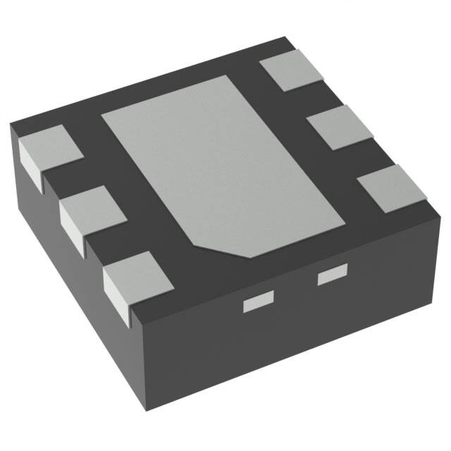
Small 2mm x 2mm SON 6-pin package
In boost mode the device provides a minimum output
current of 200mA at 3.3V VOUT from 1.8V VIN. The
boost mode is used for system components which
require a regulated supply voltage and cannot directly
operate from the input source. The boost converter is
based on a current-mode controller using
synchronous rectification to obtain maximum
efficiency and consumes typically 5.7uA from the
output. During startup of the boost converter, the
VSEL pin is read out and the integrated feedback
network sets the output voltage to 2.5V, 3V or 3.3V.
Bypass mode or boost mode operation is controlled
by the system via the EN/BYP pin.
The device integrates an enhanced bypass mode
control to prevent charge, stored in the output
capacitor during boost mode operation, from flowing
back to the input and charging the battery.
2 Applications
•
•
•
•
Metering (Gas, Water, Smart Meters)
Remote Controls
Home Security / Home Automation
Single 3V Li-MnO2 or 2 x 1.5V Alkaline Cell
Powered Applications
The device is packaged in a small 6-pin SON
package (DRV) measuring 2.0mm × 2.0mm x
0.75mm.
Device Information(1)
PART NUMBER
PACKAGE
BODY SIZE (NOM)
3 Description
TPS61291
SON (6)
2.00 mm x 2.00 mm
The TPS61291 is a boost converter with pin
selectable output voltages and an integrated bypass
mode. In bypass operation, the device provides a
direct path from the input to the system and allows a
low power micro controller (MCU) such as the
MSP430 to operate directly from a single 3V Li-MnO2
battery or dual alkaline battery cells.
(1) For all available packages, see the orderable addendum at
the end of the datasheet.
Simplified Schematic and Efficiency Curves
100
TPS61291
2 x 1.5V Alkaline /
1 x 3V Li-MnO2
+
+
-
+
-
VBAT
CIN
10mF
SW
VOUT =
Step up
converter VOUT VBAT / 3.3V
VIN
COUT
22mF
Bypass
VSEL
GND
95
Subsystem
90
VCC = 3.3V
MCU
(VCC = VBAT or 3.3V)
85
Efficiency [%]
L = 3.3mH
80
75
VIN = 1.2V
70
VIN = 1.8V
EN/BYP
65
VIN = 2.5V
60
VIN = 3.0V
55
50
0.01
0.1
1
10
100
Output Current IOUT [mA]
1
An IMPORTANT NOTICE at the end of this data sheet addresses availability, warranty, changes, use in safety-critical applications,
intellectual property matters and other important disclaimers. PRODUCTION DATA.
�TPS61291
SLVSBX9A – SEPTEMBER 2014 – REVISED SEPTEMBER 2014
www.ti.com
Table of Contents
1
2
3
4
5
6
7
Features ..................................................................
Applications ...........................................................
Description .............................................................
Revision History.....................................................
Pin Configuration and Functions .........................
Specifications.........................................................
1
1
1
2
3
4
6.1
6.2
6.3
6.4
6.5
6.6
4
4
4
4
5
6
Absolute Maximum Ratings ......................................
Handling Ratings.......................................................
Recommended Operating Conditions.......................
Thermal Information .................................................
Electrical Characteristics...........................................
Typical Characteristics ..............................................
Detailed Description .............................................. 7
7.1 Overview ................................................................... 7
7.2 Functional Block Diagram ......................................... 7
7.3 Feature Description................................................... 7
7.4 Device Functional Modes.......................................... 8
8
Applications and Implementation ...................... 10
8.1 Application Information............................................ 10
8.2 Typical Application .................................................. 10
9 Power Supply Recommendations...................... 16
10 Layout................................................................... 16
10.1 Layout Guidelines ................................................. 16
10.2 Layout Example .................................................... 16
11 Device and Documentation Support ................. 17
11.1
11.2
11.3
11.4
11.5
Device Support ....................................................
Documentation Support ........................................
Trademarks ...........................................................
Electrostatic Discharge Caution ............................
Glossary ................................................................
17
17
17
17
17
12 Mechanical, Packaging, and Orderable
Information ........................................................... 17
4 Revision History
NOTE: Page numbers for previous revisions may differ from page numbers in the current version.
Changes from Original (September 2014) to Revision A
Page
•
Changed "Bypass Mode Operation" description ................................................................................................................... 9
•
Added sub-section "Controlled Transition into Bypass Mode" .............................................................................................. 9
•
Added NOTE to the "Application and Implementation" section. .......................................................................................... 10
•
Changed "List of Inductors" table ........................................................................................................................................ 11
2
Submit Documentation Feedback
Copyright © 2014, Texas Instruments Incorporated
Product Folder Links: TPS61291
�TPS61291
www.ti.com
SLVSBX9A – SEPTEMBER 2014 – REVISED SEPTEMBER 2014
5 Pin Configuration and Functions
SW
VOUT
VIN
1
2
3
TH E
ER XP
M OS
A ED
L
PA
D
DRV Package
6 Pin
Top View
6
5
4
GND
VSEL
EN/BYP
Pin Functions
PIN
NAME
NO.
I/O
DESCRIPTION
SW
1
I
Switch node of the converter. Connect the inductor between this pin and the input capacitor
CIN.
VOUT
2
O
Boost converter output. Connect the output capacitor COUT between this pin and GND close
to the device.
VIN
3
PWR
EN/BYP
4
I
Control pin of the device. A high level enables the boost mode operation. A low level
disables the boost converter and enables bypass mode operation. EN/BYP must be actively
terminated high or low. Usually, this pin is controlled by the MCU in the system.
VSEL
5
I
Output voltage selection pin. The logic level of this pin is read out during startup and
internally latched. Connect this pin only to GND, VOUT, or leave it floating.
GND
6
PWR
EXPOSED
THERMAL
PAD
Input voltage supply pin for the boost converter. Connect the input capacitor CIN between
this pin and GND as close as possible to the device.
Ground pin of the device.
Not electrically connected to the IC, but must be soldered to achieve specified thermal
performance. Connect this pad to the GND pin and use it as a central GND plane.
NC
Output Voltage Setting
EN/BYP Pin
VSEL Pin at Startup
VOUT
Mode
high
GND
3.3V
Boost Mode Operation
high
VOUT
3.0V
high
floating
2.5V
low
GND / VOUT / floating
VOUT = VIN (Bypass Mode)
Bypass Mode Operation
Submit Documentation Feedback
Copyright © 2014, Texas Instruments Incorporated
Product Folder Links: TPS61291
3
�TPS61291
SLVSBX9A – SEPTEMBER 2014 – REVISED SEPTEMBER 2014
www.ti.com
6 Specifications
6.1 Absolute Maximum Ratings
over operating free-air temperature range (unless otherwise noted)
Pin Voltage Range
(1)
(2)
(2)
(1)
MIN
MAX
VIN
-0.3
5.5
UNIT
SW
-0.3
7
EN/BYP, VOUT
-0.3
5.5
VSEL
-0.3
VOUT +
0.3V
Output Current
In Bypass Operation (EN/BYP = GND)
TJ
Maximum Junction Temperature
-40
V
250
mA
150
°C
Stresses beyond those listed under Absolute Maximum Ratings may cause permanent damage to the device. These are stress ratings
only, which do not imply functional operation of the device at these or any other conditions beyond those indicated under Recommended
Operating Conditions. Exposure to absolute-maximum-rated conditions for extended periods may affect device reliability.
All voltage values are with respect to network ground terminal GND.
6.2 Handling Ratings
Tstg
Storage temperature range
V(ESD)
(1)
(2)
Electrostatic discharge
MIN
MAX
–65
150
-2
2
-0.5
0.5
Human body model (HBM) per ANSI/ESDA/JEDEC
JS-001, all pins (1)
Charged device model (CDM), per JEDEC
specification JESD22-C101, all pins (2)
UNIT
°C
kV
JEDEC document JEP155 states that 500-V HBM allows safe manufacturing with a standard ESD control process.
JEDEC document JEP157 states that 250-V CDM allows safe manufacturing with a standard ESD control process.
6.3 Recommended Operating Conditions
over operating free-air temperature range (unless otherwise noted)
MIN
VIN
NOM
MAX
Supply voltage for startup
1.5
Supply voltage range (once device has started)
0.9
5
VOUT
Supply voltage range for step up conversion (once device has started)
0.9
TA
Operating ambient temperature
-40
85
TJ
Operating junction temperature
–40
125
UNIT
V
°C
6.4 Thermal Information
TPS61291
THERMAL METRIC (1)
DRV (2x2 SON)
UNIT
6 PINS
RθJA
Junction-to-ambient thermal resistance
71.2
RθJCtop
Junction-to-case (top) thermal resistance
93.5
RθJB
Junction-to-board thermal resistance
46.7
ψJT
Junction-to-top characterization parameter
2.5
ψJB
Junction-to-board characterization parameter
41.1
RθJCbot
Junction-to-case (bottom) thermal resistance
11.1
(1)
4
°C/W
For more information about traditional and new thermal metrics, see the IC Package Thermal Metrics application report, SPRA953.
Submit Documentation Feedback
Copyright © 2014, Texas Instruments Incorporated
Product Folder Links: TPS61291
�TPS61291
www.ti.com
SLVSBX9A – SEPTEMBER 2014 – REVISED SEPTEMBER 2014
6.5 Electrical Characteristics
TA = –40°C to 85°C. Typical values are at TA = 25°C (unless otherwise noted)
PARAMETER
TEST CONDITIONS
MIN
TYP
MAX
UNIT
SUPPLY
VIN
IQ
Startup voltage
VOUT = 3.3V, IOUT = 20mA
Input voltage range
Operating voltage range
Quiescent current in boost mode
VIN
VOUT
Quiescent current in bypass mode
VIN
1.5
0.9
IOUT = 0 mA, VEN/BYP = VIN = 1.8 V, VOUT =
3.3V, device not switching
0.4
VEN/BYP = low, VIN = 3 V, IOUT = 0 mA
V
5
1.5
5.7
9
0.015
0.5
μA
μA
ILkSW
Leakage current into SW
VEN/BYP = low, VIN = 1.2 V, VSW = 1.2 V
0.01
0.5
VUVLO
Undervoltage lockout threshold
VIN decreasing
0.65
0.9
Overtemperature protection
TJ rising
140
°C
20
°C
Overtemperature hysteresis
V
INPUTS
IIN
EN/BYP, input current
EN/BYP = low or EN/BYP = VIN
0.01
VIN ≤ 1.5 V
VIL
EN/BYP, input low voltage
5 V > VIN > 1.5 V
VIN ≤ 1.5 V
VIH
EN/BYP, input high voltage
VIL
VSEL, input low voltage
VEN/BYP = high
VIH
VSEL, input high voltage
VEN/BYP = high
IIN
VSEL, input current
VEN/BYP = high, VSEL = VOUT = 3V
5 V > VIN > 1.5 V
0.1
μA
0.2 ×
VIN
V
0.3
0.8 ×
VIN
V
1.2
0.3
V
VOUT 0.3
V
0.01
μA
0.1
POWER SWITCHES
RDS(ON)
ISW
Rectifying switch on resistance
VOUT = 3.3 V
0.6
Ω
Main switch on resistance
VOUT = 3.3 V
0.4
Ω
Bypass switch on resistance
VIN = 1.8V, IOUT = 50 mA, EN/BYP = low
1.2
Switch current limit
VOUT = 3.3V
Output voltage accuracy
VIN = 1.8V, IOUT = 10 mA, VOUT 3.3V, 3.0V,
2.5V, EN/BYP = high
Line regulation
VOUT = 3.3V, VIN = 2V to 3.0V, IOUT = 50
mA, EN/BYP = high
Load regulation
VIN = 2V, VOUT = 3.3V, IOUT = 1 mA to 200
mA, EN/BYP = high
Output overvoltage protection
VOUT rising, EN/BYP = high
Ω
700
1000
1300
mA
-2
+1
+4
%
OUTPUT
VOUT
VOVP
+0.15
%/V
-0.007
%/mA
5.4
Submit Documentation Feedback
Copyright © 2014, Texas Instruments Incorporated
Product Folder Links: TPS61291
V
5
�TPS61291
SLVSBX9A – SEPTEMBER 2014 – REVISED SEPTEMBER 2014
www.ti.com
6.6 Typical Characteristics
0.14
1
VIN = 1.8V
VIN = 3.3V
0.8
Quiescent Current IQ into VIN [mA]
Bypass Mode Quiescent Current IQ [mA]
0.12
VIN = 1.8V
VIN = 2.5V
0.9
0.1
0.08
0.06
0.04
VIN = 2.5V
0.7
0.6
0.5
0.4
0.3
0.2
0.02
0.1
0
0
-40
-20
0
20
40
60
80
100
-40
-20
0
Temperature T A [°C]
20
40
60
80
C001
EN/BYP = low
VSEL = low
IOUT = 0mA
Figure 1. Quiescent Current IQ into VIN Pin in Bypass Mode
C001
EN/BYP = high
1.6
VIN 1.8V
VOUT = 2.6V
VOUT = 3.1V
7
1.4
VOUT = 3.4V
1.2
6
RDSON Bypass Switch [W]
Quiescent Current IQ into VOUT [mA]
Boost mode operation
Device not switching
Figure 2. Quiescent Current IQ into VIN Pin in Boost Mode
8
5
4
3
1
0.8
0.6
2
0.4
1
0.2
0
0
-40
-20
0
20
40
60
80
-40
100
-20
0
EN/BYP = high
IOUT = 0mA
40
60
80
Boost mode operation
Device not switching
100
C001
Figure 3. Quiescent Current IQ into VOUT Pin in Boost Mode
Figure 4. RDSON Bypass Switch
1
1
0.9
0.9
0.8
0.8
0.7
0.7
RDSON Rectifier Switch [W]
RDSON Main Switch [W ]
20
Temperature T A [°C]
Temperature T A [°C]]
0.6
0.5
0.4
0.3
0.6
0.5
0.4
0.3
0.2
0.2
0.1
0.1
0
0
-40
-20
0
20
40
60
80
100
-40
-20
0
20
40
60
80
100
Temperature T A [°C]
Temperature T A [°C]
VOUT = 3.3V
Figure 5. RDSON Main Switch
6
100
Temperature TA [°C]
C001
VOUT = 3.3V
Figure 6. RDSON Rectifier Switch
Submit Documentation Feedback
Copyright © 2014, Texas Instruments Incorporated
Product Folder Links: TPS61291
�TPS61291
www.ti.com
SLVSBX9A – SEPTEMBER 2014 – REVISED SEPTEMBER 2014
7 Detailed Description
7.1 Overview
The TPS61291 provides two operating modes: high efficiency boost mode to generate an output voltage higher
than the input voltage and bypass mode, which connects the output of the device directly to the input.
7.2 Functional Block Diagram
Bypass
Switch
P
VIN
SW
VOUT
N
Rectifying
Switch
VOUT
Driver
VIN
N
Bypass Switch
Control
Control Logic
EN/BYP
Main
Switch
Current
Sense
Startup Circuit
VIN
Undervoltage
Lockout
Overvoltage
Protection
BYP/EN
Reference Vref
Vref
GND
Voltage Error
Amplifier
voltage selection logic
Thermal Shutdown
VSEL
integrated FB divider
network with disconnect
7.3 Feature Description
7.3.1 Bypass / Boost Mode Operation EN/BYP
The EN/BYP pin selects the operating mode of the device. With the EN/BYP pin pulled low, the device operates
in bypass mode. With a high level on the EN/BYP pin, the device operates as a boost converter. The EN/BYP
pin is usually controlled by an I/O pin of a MCU, powered from the output of the TPS61291 and should not be left
floating. See Figure 8. See also sections Boost Mode Operation and Bypass Mode Operation for more detailed
descriptions.
Submit Documentation Feedback
Copyright © 2014, Texas Instruments Incorporated
Product Folder Links: TPS61291
7
�TPS61291
SLVSBX9A – SEPTEMBER 2014 – REVISED SEPTEMBER 2014
www.ti.com
Feature Description (continued)
7.3.2 Output Voltage Selection VSEL
In boost mode operation, the device supports three internally set output voltages: 2.5V, 3V and 3.3V. Leaving the
VSEL pin open sets the output voltage to 2.5V, VSEL = VOUT to 3.0V and VSEL= GND to 3.3V. The VSEL pin
condition is detected during the startup of the boost converter and internally latched. For proper operation, it must
be connected to either GND, VOUT or left floating. Depending on the VSEL condition, an integrated feedback
divider network is selected. Changing the VSEL pin condition during operation does not change the output
voltage.
7.3.3 Feedback Divider Disconnect
In boost mode operation, the integrated feedback divider network, which is required for regulation, is connected
to the VOUT pin. To achieve the low quiescent current in bypass mode, the integrated feedback divider network
is disconnected from the output pin VOUT.
7.3.4 Undervoltage Lockout
An undervoltage lockout function stops the operation of the boost converter if the input voltage drops below the
undervoltage lockout threshold. This function is implemented in order to prevent malfunction of the boost
converter. The undervoltage lockout function has no control of the bypass switch.
7.3.5 Overtemperature Protection
The device has a built-in temperature sensor which monitors the internal junction temperature in boost mode
operation. If the junction temperature exceeds the threshold (140 °C typical), the device stops operating. As soon
as the junction temperature has decreased below the programmed threshold, it starts operating again. There is a
built-in hysteresis to avoid unstable operation at IC temperatures at the overtemperature threshold. The
overtemperature protection is not active in bypass mode operation.
7.3.6 Overvoltage Protection
In boost mode operation (EB/BYP = high), the device features a redundant over voltage protection circuit (OVP),
which is independent from the reference, the regulation loop and feedback divider network. The redundant over
voltage protection circuit limits the output voltage to typically 5.4V. The over voltage protection can only limit the
output voltage in boost mode operation, when the input voltage VIN is smaller than the output voltage VOUT.
7.4 Device Functional Modes
7.4.1 Boost Mode Operation
The device is enabled and operates in boost mode operation when the EN/BYP pin is set high. The bypass
switch is turned off once the boost converter has started switching.
In boost mode operation, the device is controlled by a hysteretic current mode controller. This controller regulates
the output voltage by keeping the inductor ripple current constant in the range of 300 mA and adjusting the offset
of this inductor current depending on the output load. If the required average input current is lower than the
average inductor current defined by this constant ripple, the inductor current goes discontinuous to keep the
efficiency high at low load conditions. To achieve high efficiency, the power stage is realized as a synchronous
boost topology.
IL
Continuous Current Operation
IIN
Discontinuous Current Operation
Ilpp =
300 mA (typ.)
Ilpp =
300 mA (typ.)
t
Figure 7. Hysteretic Current Operation
8
Submit Documentation Feedback
Copyright © 2014, Texas Instruments Incorporated
Product Folder Links: TPS61291
�TPS61291
www.ti.com
SLVSBX9A – SEPTEMBER 2014 – REVISED SEPTEMBER 2014
Device Functional Modes (continued)
The output voltage VOUT is monitored via the integrated feedback network which is connected to the voltage error
amplifier. To regulate the output voltage, the voltage error amplifier compares this feedback voltage to the
internal voltage reference and adjusts the required offset of the inductor current accordingly.
The hysteretic current mode architecture allows fast response to load variations.
7.4.2 Bypass Mode Operation
The TPS61291 includes a P-channel MOSFET (Bypass Switch) between the VIN and VOUT pins. When the IC
is disabled (EN/BYP = low), bypass mode is activated to provide a direct, low impedance connection from the
input voltage (at the VIN pin) to the load (VOUT). The bypass switch is not impacted by undervoltage lockout, or
thermal shutdown. The bypass switch is not current-limit controlled. In bypass operation, the OVP circuit is
disabled.
7.4.3 Controlled Transition into Bypass Mode
When changing from boost mode into bypass mode, the output capacitor is usually charged up to a higher
voltage than the battery voltage VBAT. In order to prevent current flowing from the output capacitor COUT via the
bypass switch into the battery (reverse battery current), the internal bypass control circuit delays the bypass
switch activation until the output voltage VOUT has decreased to the input voltage level.
7.4.4 Operation at Output Overload
If the peak inductor current reaches the internal switch current limit threshold in boost mode operation, the main
switch is turned off to stop a further increase of the input current. In this case the output voltage will decrease
since the device cannot provide sufficient power to maintain the set output voltage. If the output voltage drops
below the input voltage, the backgate diode of the rectifying switch gets forward biased and current starts to flow
through it. Because this diode cannot be turned off, the load current is only limited by the remaining DC
resistance. As soon as the overload condition is removed, the converter automatically resumes normal operation
and enters the appropriate soft start mode depending on the operating conditions.
7.4.5 Startup
After the EN/BYP pin is tied high, the device starts to operate. If the input voltage is not high enough to supply
the control circuit properly, a startup oscillator starts to operate the switches. During this phase, the switching
frequency is controlled by the oscillator and the switch current is limited. As soon as the device has built up the
output voltage to about 1.8 V, high enough for supplying the control circuit, the device switches to its normal
hysteretic current mode operation.
Submit Documentation Feedback
Copyright © 2014, Texas Instruments Incorporated
Product Folder Links: TPS61291
9
�TPS61291
SLVSBX9A – SEPTEMBER 2014 – REVISED SEPTEMBER 2014
www.ti.com
8 Applications and Implementation
NOTE
Information in the following applications sections is not part of the TI component
specification, and TI does not warrant its accuracy or completeness. TI’s customers are
responsible for determining suitability of components for their purposes. Customers should
validate and test their design implementation to confirm system functionality.
8.1 Application Information
The TPS61291 is a boost converter with pin selectable output voltages and an integrated bypass mode. In
bypass operation, the device provides a direct path from the input to the system and allows a low power micro
controller (MCU) to operate directly from a single 3V Li-MnO2 battery or dual alkaline battery cells. In bypass
mode, the quiescent current consumption is typically only 15nA and supports low power modes of MCUs such as
the MSP430. In boost mode operation, the device provides a regulated output voltage (e.g. 3.3V) to supply
circuits which require a higher voltage than provided by the battery. See Figure 8.
The device also extends battery life in applications which can run partially directly from the battery, but need a
boost conversion to maintain sufficient system voltage when the battery voltage drops due to discharge. In this
case, the system runs off the battery in bypass mode operation until the battery voltage trips the minimum
system operating voltage. Then the system turns on the boost converter, providing a sufficient output voltage
down to the cut off voltage of the battery. See Figure 9 and Figure 26.
8.2 Typical Application
TPS61291
L = 3.3mH
2 x 1.5V Alkaline /
1 x 3V Li-MnO2
+
+
-
Subsystem
VOUT =
Step up
converter VOUT VBAT / 3.3V
VIN
COUT
22mF
Bypass
CIN
10mF
+
-
SW
VCC = 3.3V
MCU
(VCC = VBAT or 3.3V)
VSEL
GND
EN/BYP
Figure 8. Typical Application Circuit with Regulated 3.3V VOUT / VBAT
System
TPS61291
L = 3.3mH
2 x 1.5V Alkaline /
1 x 3V Li-MnO2
+
+
-
VBAT
CIN
+
-
NC
SW
VOUT =
Step up
V
/ 2.5V
BAT
converter VOUT
VIN
COUT
Bypass
MCU + ADC
Subsystem
VSEL
GND
EN/BYP
EN/BYP set high
@ VBAT = 2.2V
Minimum VCC for System: 2.2V
Bypass Mode:
VOUT = VBAT (for VBAT > 2.2V)
Boost Mode:
VOUT = 2.5V (for VBAT < 2.2V)
Figure 9. Bypass Mode / Boost Mode Operation to Maintain Sufficient System Voltage
8.2.1 Design Requirements
The TPS61291 is a highly integrated boost converter. The output voltage is set internally via a VSEL pin without
any additional components. For operation, only an input capacitor, output capacitor, and an inductor are required.
Table 1 shows the components used for the application characteristic curves.
10
Submit Documentation Feedback
Copyright © 2014, Texas Instruments Incorporated
Product Folder Links: TPS61291
�TPS61291
www.ti.com
SLVSBX9A – SEPTEMBER 2014 – REVISED SEPTEMBER 2014
Typical Application (continued)
Table 1. Components for Application Characteristic Curves (1)
(1)
Reference
Description
TPS61291
Low Iq Boost Converter with
Bypass Operation
Value
Manufacturer
Texas Instruments
CIN
Input capacitor
10µF
Murata
GRM219R61A106KE44D
COUT
Output capacitor
22µF
Murata
GRM21BR60J226ME39L
L
Inductor
3.3µH
Coilcraft
LPS3314 3R3
See the Third-Party Products Disclaimer in the Device Support section.
8.2.2 Detailed Design Procedure
The external components have to fulfill the needs of the application but also the stability criteria of the device's
control loop. The TPS61291 is optimized to work within a range of L and C combinations. The LC output filter
inductance and capacitance must be considered together. The output capacitor sets the corner frequency of the
converter while the inductor creates a Right-Half-Plane-Zero degrading the stability of the converter.
Consequently with a larger inductor a bigger capacitor has to be used to guarantee a stable loop. Table 2 shows
the output filter component selection.
Table 2. Recommended LC Output Filter Combinations
Output voltage
[V]
3.3 / 3.0
2.5
(1)
(2)
(3)
Output capacitor value [µF] (2)
Inductor value [µH] (1)
22
22 + 10
2 x 22
(3)
√
√
√
√
√
(3)
√
√
3.3
√
4.7
2.2
√
3.3
Inductor tolerance and current de-rating is anticipated. The effective inductance can vary by 20% and -30%.
Capacitance tolerance and bias voltage de-rating is anticipated. The effective capacitance can vary by 20% and -50%.
This LC combination is the standard value and recommended for most applications.
8.2.2.1 Inductor Selection
The device is optimized to operate with a 3.3µH inductor value. Other inductor values can be used, per Table 2.
The maximum inductor current can be approximated by the ILMAX, from Equation 1. For proper operation, the
inductor needs to be rated for a saturation current which is higher than the switch current limit of typically 1A.
Table 3 lists inductors that have been tested with the TPS61291.
V
´I
IL max : = OUT OUT + 150 mA continuous current operation
0.8 ´ VIN
IL max : = 300 mA
discontinuous current operation
(1)
Table 3. List of Inductors (1)
(1)
INDUCTANCE
DIMENSIONS [mm3]
TYPE
3.3
3.3 x 3.3 x 1.3
LPS3314
3.3
2.95 x 2.95 x 1.4
LPS3015
3.3
3 x 2.5 x 1.5
VLF302515
TDK
3.3
2 x 2 x 1.2
MDMK2020T3R3M
Taiyo Yuden
3.3
2.5 x 2.0 x 1.2
DFE252012
Toko
3.3
3.0 x 3.0 x 1.5
74438335033
Würth
SUPPLIER
Coilcraft
See the Third-Party Products Disclaimer in the Device Support section.
Submit Documentation Feedback
Copyright © 2014, Texas Instruments Incorporated
Product Folder Links: TPS61291
11
�TPS61291
SLVSBX9A – SEPTEMBER 2014 – REVISED SEPTEMBER 2014
www.ti.com
8.2.2.2 Input and Output Capacitor Selection
For best output and input voltage filtering, low ESR X5R or X7R ceramic capacitors are recommended. The input
capacitor minimizes input voltage ripple, suppresses input voltage spikes and provides a stable system rail for
the device. At least a 10μF or larger input capacitor is recommended for operation. In applications in which the
power source (e.g. certain battery chemistries) shows an internal resistance characteristic, a larger input
capacitor might be used to buffer the supply voltage for the TPS61291. The recommended typical output
capacitor value is 22 μF and can vary as outlined in the output filter selection Table 2.
12
Submit Documentation Feedback
Copyright © 2014, Texas Instruments Incorporated
Product Folder Links: TPS61291
�TPS61291
www.ti.com
SLVSBX9A – SEPTEMBER 2014 – REVISED SEPTEMBER 2014
100
100
95
95
90
90
85
85
Efficiency [%]
Efficiency [%]
8.2.3 Application Curves
80
75
VIN = 1.2V
70
80
75
VIN = 1.2V
70
VIN = 1.8V
VIN = 1.8V
65
VIN = 2.5V
60
VIN = 3.0V
VIN = 2.5V
65
VIN = 2.7V
60
55
55
50
0.01
0.1
1
10
50
0.01
100
0.1
1
10
100
Output Current IOUT [mA]
Output Current IOUT [mA]
C002
C002
EN/BYP = high
L = 3.3µH
VSEL = GND
EN/BYP = high
L = 3.3µH
VSEL = VOUT
Figure 11. Efficiency vs IOUT, VOUT = 3.0V
Figure 10. Efficiency vs IOUT, VOUT = 3.3V
100
3.399
95
Output Voltage VOUT [V]
90
Efficiency [%]
85
80
75
VIN = 1.2V
70
VIN = 1.8V
65
3.366
3.333
VIN = 1.2V
VIN = 1.8V
VIN = 2.2V
3.300
VIN = 2.5V
60
VIN = 3.0V
55
50
0.01
0.1
1
10
3.267
0.01
100
0.1
Output Current IOUT [mA]
1
10
100
Output Current IOUT[mA]
C006
C001
EN/BYP = high
L = 3.3µH
VSEL = open
3.090
2.575
3.060
2.550
3.030
VIN = 1.2V
3.000
L = 3.3µH
2.525
VIN = 1.2V
VIN = 1.8V
2.500
VIN = 1.8V
VIN = 2.2V
VIN = 2.5V
2.970
0.01
0.1
1
10
2.475
0.01
100
Output Current IOUT [mA]
0.1
1
10
L = 3.3µH
100
Output Current IOUT [mA]
C005
EN/BYP = high
VSEL = GND
Figure 13. Output Voltage vs Output Current VOUT = 3.3V
Output Voltage VOUT [V]
Output Voltage VOUT [V]
Figure 12. Efficiency vs IOUT, VOUT = 2.5V
EN/BYP = high
VSEL = VOUT
Figure 14. Output Voltage vs Output Current VOUT = 3.0V
C004
EN/BYP = high
L = 3.3µH
VSEL = open
Figure 15. Output Voltage vs Output Current VOUT = 2.5V
Submit Documentation Feedback
Copyright © 2014, Texas Instruments Incorporated
Product Folder Links: TPS61291
13
�TPS61291
SLVSBX9A – SEPTEMBER 2014 – REVISED SEPTEMBER 2014
www.ti.com
35
0.600
T A = 25°C
T A = 85°C
25
0.400
0.300
Input Current IIN [uA]
Maximum Output Current IOUTMAX [A]
T A = -40°C
30
0.500
VOUT = 2.5V
VOUT = 3.0V
VOUT = 3.3V
0.200
20
15
10
0.100
5
0.000
0
0.5
1.0
1.5
2.0
2.5
3.0
3.5
0.9
1.4
1.9
Input Voltage VIN [V]
2.4
2.9
Input Voltage VIN [V]
C001
EN/BYP = high
L = 3.3µH
ISW = 1000mA (typical)
Boost mode operation
Figure 16. Maximum Output Current
VOUT = 3.3 V
IOUT = 0 mA
L = 3.3 µH
COUT = 22 µF
Device switching
Figure 17. Supply Current vs. VIN, VOUT = 3.3V, IOUT = 0mA
35
30
T A = 25°C
T A = 25°C
T A = -40°C
30
T A = -40°C
25
T A = 85°C
T A = 85°C
Input Current IIN [uA]
Input Current IIN [uA]
25
20
15
20
15
10
10
5
5
0
0
0.9
1.4
1.9
2.4
2.9
0.9
1.4
Input Voltage VIN [V]
VOUT = 3.0 V
IOUT = 0 mA
L = 3.3 µH
COUT = 22 µF
Device switching
Figure 18. Supply Current vs. VIN, VOUT = 3.0V, IOUT = 0mA
VIN = 2.0 V
VOUT = 3.3 V
L = 3.3 µH
IOUT = 15mA
VOUT = 2.5 V
IOUT = 0 mA
2.4
L = 3.3 µH
COUT = 22 µF
Device switching
Figure 19. Supply Current vs. VIN, VOUT = 2.5V, IOUT = 0mA
COUT = 22 µF
VSEL = GND
EN/BYP = high
Figure 20. Discontinuous Conduction Mode Operation,
VOUT = 3.3V
14
1.9
Input Voltage VIN [V]
VIN = 1.8 V
VOUT = 3.3 V
VSEL = GND
L = 3.3 µH
COUT = 22 µF
IOUT = 150 mA
EN/BYP = high
Figure 21. Continuous Conduction Mode Operation,
VOUT = 3.3V
Submit Documentation Feedback
Copyright © 2014, Texas Instruments Incorporated
Product Folder Links: TPS61291
�TPS61291
www.ti.com
SLVSBX9A – SEPTEMBER 2014 – REVISED SEPTEMBER 2014
VIN = 1.8V
VOUT = 3.3V
L = 3.3µH
COUT = 22 µF
VSEL = GND
ILOAD 20mA /150mA
VIN = 1.8V
VOUT = 3.3V
Figure 22. Load Transient Response
L = 3.3µH
COUT = 22 µF
VSEL = GND
ILOAD 1mA/200mA
Figure 23. AC Load Sweep
Boost operation
Bypass switch activation
when VOUT is discharged to VIN level
Bypass mode
VIN = 2.5V/3V
VOUT = 3.3V
L = 3.3µH
VSEL = GND
COUT = 22 µF
Load =100Ω
Figure 24. Line Transient Response
VIN = 2.0V
VOUT = 3.3V
L = 3.3µH
VSEL = GND
COUT = 22 µF
RLOAD = 1kΩ
Figure 25. Boost Mode / Bypass Mode Transition
VIN
VOUT = 2.5V
VOUT
tracks VIN
VIN < 2.2V
EN/BYP control
IL
VIN = 0.9V to 3V
VOUT = 2.5V
VSEL = Open
ILOAD = 5mA
EN/BYP externally controlled
Bypass / Boost mode operation
VIN = 2.0V
VOUT = 3.3V
Figure 26. Bypass / Boost Mode Operation
L = 3.3µH
VSEL = GND
COUT = 22 µF
RLOAD = 100Ω
Figure 27. Startup in Boost Mode
Submit Documentation Feedback
Copyright © 2014, Texas Instruments Incorporated
Product Folder Links: TPS61291
15
�TPS61291
SLVSBX9A – SEPTEMBER 2014 – REVISED SEPTEMBER 2014
www.ti.com
9 Power Supply Recommendations
The input power supply needs to have a current rating according to the supply voltage, output voltage and output
current of the TPS61291.
10 Layout
10.1 Layout Guidelines
As for all switching power supplies, the layout is an important step in the design. Care must be taken in board
layout to get the specified performance. If the layout is not carefully done, the regulator could show poor line
and/or load regulation, stability issues as well as EMI problems. It is critical to provide a low inductance, low
impedance ground path. Therefore, use wide and short traces for the main current paths. In a boost converter,
the ripple current on the output is larger than the ripple current on the input. The output capacitor needs to be
placed as close as possible between the VOUT and the GND pins. The input capacitor should be placed as
close as possible to the VIN and GND pins. Place the inductor close by the IC and connect it with short and thick
traces to the IC. Avoid current loops to minimize radiated noise and stray fields. The exposed thermal pad of the
package and the GND pin must be connected. See Figure 28 for the recommended PCB layout.
10.2 Layout Example
2
Area: ~ 51 mm
VIN
VOUT
GND
U1
CIN
L
GND
COUT
Figure 28. Recommended PCB Layout
16
Submit Documentation Feedback
Copyright © 2014, Texas Instruments Incorporated
Product Folder Links: TPS61291
�TPS61291
www.ti.com
SLVSBX9A – SEPTEMBER 2014 – REVISED SEPTEMBER 2014
11 Device and Documentation Support
11.1 Device Support
11.1.1 Third-Party Products Disclaimer
TI'S PUBLICATION OF INFORMATION REGARDING THIRD-PARTY PRODUCTS OR SERVICES DOES NOT
CONSTITUTE AN ENDORSEMENT REGARDING THE SUITABILITY OF SUCH PRODUCTS OR SERVICES
OR A WARRANTY, REPRESENTATION OR ENDORSEMENT OF SUCH PRODUCTS OR SERVICES, EITHER
ALONE OR IN COMBINATION WITH ANY TI PRODUCT OR SERVICE.
11.2 Documentation Support
11.2.1 Related Documentation
TPS61291EVM-569 User's Guide, SLVUA29
11.3 Trademarks
11.4 Electrostatic Discharge Caution
These devices have limited built-in ESD protection. The leads should be shorted together or the device placed in conductive foam
during storage or handling to prevent electrostatic damage to the MOS gates.
11.5 Glossary
SLYZ022 — TI Glossary.
This glossary lists and explains terms, acronyms, and definitions.
12 Mechanical, Packaging, and Orderable Information
The following pages include mechanical packaging and orderable information. This information is the most
current data available for the designated devices. This data is subject to change without notice and revision of
this document. For browser-based versions of this data sheet, refer to the left-hand navigation.
Submit Documentation Feedback
Copyright © 2014, Texas Instruments Incorporated
Product Folder Links: TPS61291
17
�PACKAGE OPTION ADDENDUM
www.ti.com
10-Dec-2020
PACKAGING INFORMATION
Orderable Device
Status
(1)
Package Type Package Pins Package
Drawing
Qty
Eco Plan
(2)
Lead finish/
Ball material
MSL Peak Temp
Op Temp (°C)
Device Marking
(3)
(4/5)
(6)
TPS61291DRVR
ACTIVE
WSON
DRV
6
3000
RoHS & Green
NIPDAU
Level-2-260C-1 YEAR
-40 to 85
PC4I
TPS61291DRVT
ACTIVE
WSON
DRV
6
250
RoHS & Green
NIPDAU
Level-2-260C-1 YEAR
-40 to 85
PC4I
(1)
The marketing status values are defined as follows:
ACTIVE: Product device recommended for new designs.
LIFEBUY: TI has announced that the device will be discontinued, and a lifetime-buy period is in effect.
NRND: Not recommended for new designs. Device is in production to support existing customers, but TI does not recommend using this part in a new design.
PREVIEW: Device has been announced but is not in production. Samples may or may not be available.
OBSOLETE: TI has discontinued the production of the device.
(2)
RoHS: TI defines "RoHS" to mean semiconductor products that are compliant with the current EU RoHS requirements for all 10 RoHS substances, including the requirement that RoHS substance
do not exceed 0.1% by weight in homogeneous materials. Where designed to be soldered at high temperatures, "RoHS" products are suitable for use in specified lead-free processes. TI may
reference these types of products as "Pb-Free".
RoHS Exempt: TI defines "RoHS Exempt" to mean products that contain lead but are compliant with EU RoHS pursuant to a specific EU RoHS exemption.
Green: TI defines "Green" to mean the content of Chlorine (Cl) and Bromine (Br) based flame retardants meet JS709B low halogen requirements of