Order
Now
Product
Folder
Support &
Community
Tools &
Software
Technical
Documents
TPS61500
SLVS893F – DECEMBER 2008 – REVISED MAY 2019
TPS61500 High-Brightness, LED Driver With Integrated 3-A, 40-V Power Switch
1 Features
•
•
1
•
•
•
•
•
•
The LED current is set with an external sensor
resistor R3, and the feedback voltage that is
regulated to 200 mV by current mode PWM (pulse
width modulation) control loop, as shown in Typical
Application Circuit. The device supports analog and
pure PWM dimming methods for LED brightness
control. Connecting a capacitor to the DIMC pin
configures the device to be used for analog dimming,
and the LED current varies proportional to the duty
cycle of an external PWM signal. Floating the DIMC
pin configures the device for pure PWM dimming with
the average LED current being the PWM signal's duty
cycle times a set LED current.
2.9-V to 18-V Input Voltage Range
3-A, 40-V Internal Power Switch
– Four 3-W LEDs From 5-V Input
– Eight 3-W LEDs From 12-V Input
High-Efficiency Power Conversion: Up to 93%
Frequency Set by External Resistor: 200 kHz to
2.2 MHz
User-Defined Soft Start Into Full Load
Programmable Overvoltage Protection
Analog and Pure PWM Brightness Dimming
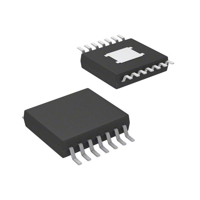
14-Pin HTSSOP Package With PowerPAD™
The device features a programmable soft-start
function to limit inrush current during start-up, and it
has other built-in protection features, such as pulseby-pulse overcurrent limit, overvoltage protection, and
thermal shutdown. The TPS61500 is available in 14pin HTSSOP package with PowerPAD.
2 Applications
•
•
Monitor Backlight
1-W or 3-W High-Brightness LED
Device Information(1)
3 Description
PART NUMBER
The TPS61500 is a monolithic switching regulator
with integrated 3-A, 40-V power switch. It is an ideal
driver for high brightness 1-W or 3-W LED. The
device has a wide input voltage range to support
application with input voltage from multi-cell batteries
or regulated 5-V or 12-V power rails.
TPS61500
PACKAGE
HTSSOP (14)
BODY SIZE (NOM)
5.00 mm × 4.40 mm
(1) For all available packages, see the orderable addendum at
the end of the data sheet.
Typical Application Circuit
D1
L1
Vin 5 V
C1
TPS61500
VIN
SW
EN
SW
R1
DL1
3W LED
C2
DL2
PWM
C4
COMP
OVP
DIMC
FB
FREQ
PGND
SS
PGND
AGND
PGND
R2
DL3
DL4
C5
R4
C3
R3
1
An IMPORTANT NOTICE at the end of this data sheet addresses availability, warranty, changes, use in safety-critical applications,
intellectual property matters and other important disclaimers. PRODUCTION DATA.
�TPS61500
SLVS893F – DECEMBER 2008 – REVISED MAY 2019
www.ti.com
Table of Contents
1
2
3
4
5
6
7
Features ..................................................................
Applications ...........................................................
Description .............................................................
Revision History.....................................................
Pin Configuration and Functions .........................
Specifications.........................................................
1
1
1
2
3
4
6.1
6.2
6.3
6.4
6.5
6.6
4
4
4
5
5
7
Absolute Maximum Ratings .....................................
ESD Ratings..............................................................
Recommended Operating Conditions.......................
Thermal Information ..................................................
Electrical Characteristics...........................................
Typical Characteristics ..............................................
Detailed Description .............................................. 9
7.1 Overview ................................................................... 9
7.2 Functional Block Diagram ......................................... 9
7.3 Feature Description................................................. 10
7.4 Device Functional Modes........................................ 11
8
Application and Implementation ........................ 12
8.1 Application Information............................................ 12
8.2 Typical Applications ................................................ 12
9 Power Supply Recommendations...................... 18
10 Layout................................................................... 18
10.1 Layout Guidelines ................................................. 18
10.2 Layout Example .................................................... 18
10.3 Thermal Considerations ........................................ 19
11 Device and Documentation Support ................. 20
11.1
11.2
11.3
11.4
Device Support......................................................
Trademarks ...........................................................
Electrostatic Discharge Caution ............................
Glossary ................................................................
20
20
20
20
12 Mechanical, Packaging, and Orderable
Information ........................................................... 20
4 Revision History
NOTE: Page numbers for previous revisions may differ from page numbers in the current version.
Changes from Revision E (March 2018) to Revision F
•
Page
Editorial changes only, no technical revisions ....................................................................................................................... 1
Changes from Revision D (June 2017) to Revision E
Page
•
Changed ground symbol of R3 change from PGND to AGND in Typical Application Circuit ................................................ 1
•
Changed ground symbol of R3 change from PGND to AGND in Figure 7 .......................................................................... 12
•
Changed ground symbol of R3 change from PGND to AGND in Figure 11 ........................................................................ 17
Changes from Revision C (March 2015) to Revision D
Page
•
Changed "Analog and PWM dimming frequency" to "PWM dimming frequency" in ROC table; add separate row for
"Analog dimming frequency"................................................................................................................................................... 4
•
Added sentence at end of Analog Dimming Method ........................................................................................................... 11
Changes from Revision B (March 2012) to Revision C
•
Added Pin Configuration and Functions section, ESD Ratings table, Feature Description section, Device Functional
Modes, Application and Implementation section, Power Supply Recommendations section, Layout section, Device
and Documentation Support section, and Mechanical, Packaging, and Orderable Information section .............................. 1
Changes from Revision A (February 2012) to Revision B
•
2
Page
Changed the ORDERING INFORMATION table PACKAGE MARKING From: TPS61500PWP To: 61500 ........................ 1
Changes from Original (December 2008) to Revision A
•
Page
Page
Replaced the Dissipation Ratings Table with Thermal Information........................................................................................ 4
Submit Documentation Feedback
Copyright © 2008–2019, Texas Instruments Incorporated
Product Folder Links: TPS61500
�TPS61500
www.ti.com
SLVS893F – DECEMBER 2008 – REVISED MAY 2019
5 Pin Configuration and Functions
PWP Package
14-Pin HTSSOP With Thermal Pad
Top View
Pin Functions
PIN
I/O
DESCRIPTION
NAME
NO.
AGND
7
I
Signal ground of the IC
COMP
8
O
Output of the transconductance error amplifier. An external RC network is connected to this pin.
6
I
Analog and PWM dimming method option pin. A capacitor connected to the pin to set the time constant
of reference for analog dimming. Float this pin for PWM dimming.
4
I
Enable pin. When the voltage of this pin falls below the enable threshold for more than 10 ms, the IC
turns off. This pin is also used for PWM signal input for LED brightness dimming.
9
I
Feedback pin for positive voltage regulation. A resistor connects to this pin to program LED current.
10
O
Switch frequency program pin. An external resistor is connected to this pin. See Application Information
for information on how to size the FREQ resistor.
11
I
Overvoltage protection for LED driver. The voltage is 1.229 V. Using a resistor divider can program the
threshold of OVP.
12-14
I
Power ground of the IC. It is connected to the source of the PWM switch.
5
O
Soft start programming pin. A capacitor between the SS pin and GND pin programs soft-start timing. See
Application and Implementation for information on how to size the SS capacitor
1, 2
I
This is the switching node of the IC. Connect SW to the switched side of the inductor.
—
—
3
I
DIMC
EN
FB
FREQ
OVP
PGND
SS
SW
Thermal Pad
VIN
Solder the thermal pad to the analog ground. If possible, use thermal via to connect to top and internal
ground plane layers for ideal power dissipation.
The input pin to the IC. Connect VIN to a supply voltage between 2.9 V and 18 V. It is acceptable for the
voltage on the pin to be different from the boost power stage input for applications requiring voltage
beyond VIN range.
Submit Documentation Feedback
Copyright © 2008–2019, Texas Instruments Incorporated
Product Folder Links: TPS61500
3
�TPS61500
SLVS893F – DECEMBER 2008 – REVISED MAY 2019
www.ti.com
6 Specifications
6.1 Absolute Maximum Ratings
over operating free-air temperature range (unless otherwise noted)
(1)
Supply voltages on pin VIN (2)
Voltages on pins EN
(2)
MIN
MAX
UNIT
–0.3
20
V
–0.3
20
V
Voltage on pin FB, FREQ and COMP, OVP (2)
–0.3
3
V
Voltage on pin DIMC, SS (2)
–0.3
7
V
–0.3
40
V
Voltage on pin SW
(2)
Continuous power dissipation
See Thermal Information
Operating junction temperature
–40
150
°C
Storage temperature, Tstg
–65
150
°C
(1)
(2)
Stresses beyond those listed under Absolute Maximum Ratings may cause permanent damage to the device. These are stress ratings
only and functional operation of the device at these or any other conditions beyond those indicated under Recommended Operating
Conditions is not implied. Exposure to absolute-maximum-rated conditions for extended periods may affect device reliability.
All voltage values are with respect to network ground terminal.
6.2 ESD Ratings
VALUE
V(ESD)
(1)
(2)
Electrostatic discharge
Human body model (HBM), per ANSI/ESDA/JEDEC JS-001 (1)
±2000
Charged-device model (CDM), per JEDEC specification JESD22-C101 (2)
±500
UNIT
V
JEDEC document JEP155 states that 500-V HBM allows safe manufacturing with a standard ESD control process.
JEDEC document JEP157 states that 250-V CDM allows safe manufacturing with a standard ESD control process.
6.3 Recommended Operating Conditions
MIN
NOM
MAX
UNIT
VIN
Input voltage
2.9
18
VO
Output voltage
VIN
38
V
L
Inductor (1)
4.7
47
μH
CI
Input capacitor
4.7
—
μF
CO
Output capacitor
4.7
10
μF
Cdim
Analog dimming capacitor (2)
0.1
—
μF
200
1000
Analog dimming frequency (3)
200
40 000
TA
Operating ambient temperature
–40
85
°C
TJ
Operating junction temperature
–40
125
°C
PWM
(1)
(2)
(3)
4
PWM dimming frequency
(3)
V
Hz
The inductance value depends on the switching frequency and end applications. While larger values may be used, values between 4.7
μH and 47 μH have been successfully tested in various applications. Refer to Selecting the Inductor for details.
The Cdim with the internal resistor (25 kΩ typical) forms a RC filter that generates the FB reference voltage according to the duty cycle
of PWM signal. To optimize the RC filter and reduce the output ripple, the value larger than 0.1 μF of Cdim is recommended.
When analog dimming, the maximum PWM frequency is set by on the RC filter to optimize the output ripple. When PWM dimming, the
PWM frequency is set by the device loop response.
Submit Documentation Feedback
Copyright © 2008–2019, Texas Instruments Incorporated
Product Folder Links: TPS61500
�TPS61500
www.ti.com
SLVS893F – DECEMBER 2008 – REVISED MAY 2019
6.4 Thermal Information
TPS61500
THERMAL METRIC (1)
PWP (HTSSOP)
UNIT
14 PINS
RθJA
Junction-to-ambient thermal resistance
45.2
°C/W
RθJC(top)
Junction-to-case (top) thermal resistance
34.9
°C/W
RθJB
Junction-to-board thermal resistance
30.1
°C/W
ψJT
Junction-to-top characterization parameter
1.5
°C/W
ψJB
Junction-to-board characterization parameter
29.9
°C/W
RθJC(bot)
Junction-to-case (bottom) thermal resistance
5.8
°C/W
(1)
For more information about traditional and new thermal metrics, see the Semiconductor and IC Package Thermal Metrics application
report.
6.5 Electrical Characteristics
FSW = 1.2 MHz (Rfreq = 80 kΩ), Vin = 3.6 V, CRTL = Vin, TA = –40°C to +85°C, typical values are at TA = 25°C (unless
otherwise noted)
PARAMETER
TEST CONDITIONS
MIN
TYP
MAX
UNIT
SUPPLY CURRENT
VIN
Input voltage range
IQ
Operating quiescent current into VIN
ISD
2.9
18
V
Device PWM switching without load, VIN =
3.6 V
3.5
mA
Shutdown current
EN = GND, VIN = 3.6 V
1.5
μA
VUVLO
Undervoltage lockout threshold
VIN falling
Vhys
Undervoltage lockout hysteresis
2.5
2.7
V
130
mV
ENABLE AND REFERENCE CONTROL
Venh
EN logic high voltage
VIN = 2.9 V to 18 V
Venl
EN logic low voltage
VIN = 2.9 V to 18 V
Ren
EN pulldown resistor
Toff
Shutdown delay, SS discharge
1.2
0.4
400
EN high to low
V
800
V
1600
kΩ
10
ms
VOLTAGE AND CURRENT CONTROL
VREF
Voltage feedback regulation voltage
IFB
Voltage feedback input bias current
VEA_OFF
Error amplifier offset
Isink
COMP pin sink current
VFB = VREF + 200 mV, VCOMP = 1 V
40
μA
Isource
COMP pin source current
VFB = VREF –200 mV, VCOMP = 1 V
40
μA
VCCLP
COMP pin clamp voltage
VCTH
COMP pin threshold
Gea
Error amplifier transconductance
Rea
Error amplifier output resistance
fea
Error amplifier crossover frequency
195
–10
200
0
High clamp
3
Low clamp
0.75
Duty cycle = 0%
205
mV
200
nA
10
mV
V
0.95
240
340
V
440
μmho
10
MΩ
500
kHz
Submit Documentation Feedback
Copyright © 2008–2019, Texas Instruments Incorporated
Product Folder Links: TPS61500
5
�TPS61500
SLVS893F – DECEMBER 2008 – REVISED MAY 2019
www.ti.com
Electrical Characteristics (continued)
FSW = 1.2 MHz (Rfreq = 80 kΩ), Vin = 3.6 V, CRTL = Vin, TA = –40°C to +85°C, typical values are at TA = 25°C (unless
otherwise noted)
PARAMETER
TEST CONDITIONS
MIN
TYP
MAX
UNIT
0.26
1.4
2.64
MHz
FREQUENCY
fS
Oscillator frequency
Rfreq = 480 kΩ
Rfreq = 80 kΩ
Rfreq = 40 kΩ
0.16
1.0
1.76
0.21
1.2
2.2
Dmax
Maximum duty cycle
Rfreq = 80 kΩ
89%
93%
VFREQ
FREQ pin voltage
Tmin_on
Minimum on pulse width
Rdim_fil
Dimming filter resistance
Rfreq = 80 kΩ
1.229
V
60
ns
25
kΩ
POWER SWITCH
RDS(ON)
N-channel MOSFET on-resistance
ILN_NFET
N-channel leakage current
VIN = VGS = 3.6 V
0.13
VIN = VGS = 3 V
0.25
0.3
VDS = 40 V, TA = 25°C
1
Ω
μA
OC, OVP and SS
ILIM
N-Channel MOSFET current limit
D = Dmax
ISS
Soft-start bias current
Vss = 0 V
VOVP
Overvoltage protection threshold
VOVP_hys
Overvoltage protection hysteresis
3
3.8
5
6
1.192
1.229
A
μA
1.266
V
40
mV
THERMAL SHUTDOWN
Tshutdown
Thermal shutdown threshold
160
°C
Thysteresis
Thermal shutdown threshold
hysteresis
15
°C
6
Submit Documentation Feedback
Copyright © 2008–2019, Texas Instruments Incorporated
Product Folder Links: TPS61500
�TPS61500
www.ti.com
SLVS893F – DECEMBER 2008 – REVISED MAY 2019
6.6 Typical Characteristics
Table 1. Table of Graphs
FIGURE
Efficiency
VIN = 5 V, 4 LEDs, 8 LEDs, 10 LEDs
Figure 1
Efficiency
VIN = 5 V, 12 V; VOUT = 8 LEDs
Figure 2
FB voltage accuracy
vs Temperature
Figure 3
Switch current limit
vs Duty cycle
Figure 4
Switch current limit
vs Temperature
Figure 5
Circuit of Typical Application Circuit ; L1 = D104C2-10 μH; D1 = SS3P6L-E3/86A, R4 = 80 kΩ, C4 = 470 nF, C2 = 10 μF, LED
= OSRAM LCW W5SM, ILED = 400 mA; unless otherwise noted.
100
100
VI = 5 V
VI = 12 V
4 LEDs
90
90
VI = 5 V
Efficiency - %
Efficiency - %
8 LEDs
80
10 LEDs
70
80
70
8 LEDs
60
60
50
50
0
0.2
0.4
0.6
0.8
IO - Output Current - A
1
0
1.2
0.2
0.4
0.6
0.8
IO - Output Current - A
5
205
4.5
Overcurrent Limit - A
FB Voltage - mV
1.2
Figure 2. Efficiency
Figure 1. Efficiency
210
200
195
190
-40
1
4
3.5
-20
0
20
40
60
80
TA - Free-Air Temperature - °C
100
120
3
0.2
Figure 3. FB Voltage Accuracy
0.4
0.6
Duty Cycle - %
0.8
Figure 4. Switch Current Limit
Submit Documentation Feedback
Copyright © 2008–2019, Texas Instruments Incorporated
Product Folder Links: TPS61500
1
7
�TPS61500
SLVS893F – DECEMBER 2008 – REVISED MAY 2019
www.ti.com
Circuit of Typical Application Circuit ; L1 = D104C2-10 μH; D1 = SS3P6L-E3/86A, R4 = 80 kΩ, C4 = 470 nF, C2 = 10 μF, LED
= OSRAM LCW W5SM, ILED = 400 mA; unless otherwise noted.
4
Overcurrent Limit - A
3.9
3.8
3.7
3.6
3.5
-40
-20
0
80
60
20
40
TA - Free-Air Temperature - °C
100
120
Figure 5. Switch Current Limit
8
Submit Documentation Feedback
Copyright © 2008–2019, Texas Instruments Incorporated
Product Folder Links: TPS61500
�TPS61500
www.ti.com
SLVS893F – DECEMBER 2008 – REVISED MAY 2019
7 Detailed Description
7.1 Overview
The TPS61500 integrates a 3-A, 40-V low side switch FET for driving up to 10 high-brightness LEDs in series.
The device regulates the FB pin voltage at 200 mV with current mode pulse width modulation (PWM) control,
and the LED current is sensed through a low-value resistor in series with LEDs.
The PWM control circuitry turns on the switch at the beginning of each switching cycle. The input voltage is
applied across the inductor and stores the energy as inductor current ramps up. During this portion of the
switching cycle, the load current is provided by the output capacitor. When the inductor current rises to the
threshold set by the error amplifier output, the power switch turns off and the external Schottky diode is forward
biased. The inductor transfers stored energy to replenish the output capacitor and supply the load current. This
operation repeats each switching cycle. As shown in Functional Block Diagram, the duty cycle of the converter is
determined by the PWM control comparator which compares the error amplifier output and the current signal.
The switching frequency is programmed by the external resistor.
A ramp signal from the oscillator is added to the current ramp. This slope compensation is necessary to avoid
sub-harmonic oscillation that is intrinsic to the current mode control at duty cycle higher than 50%. The feedback
loop regulates the FB pin to a reference voltage through an error amplifier. The output of the error amplifier is
connected to the COMP pin. An external compensation network is connected to the COMP pin to optimize the
feedback loop for stability and transient response.
7.2 Functional Block Diagram
OVP
VIN
SW
FB
EN
1.229 V Ref.
DIMC
200 mV Ref.
and
Dimming
EA
Gate
Dirver
COMP
PWM Control
Ramp
Generator
Current
Sensor
+
Oscillator
SS
AGND
FREQ
PGND
Submit Documentation Feedback
Copyright © 2008–2019, Texas Instruments Incorporated
Product Folder Links: TPS61500
9
�TPS61500
SLVS893F – DECEMBER 2008 – REVISED MAY 2019
www.ti.com
7.3 Feature Description
7.3.1 Switching Frequency
The switch frequency is determined by a resistor connected to the FREQ pin of the TPS61500. Do not leave this
pin open. A resistor must always be connected for proper operation. See Table 2 and Figure 6 for resistor values
and corresponding frequencies.
Table 2. Switching Frequency vs External Resistor
R4 (kΩ)
fSW (kHz)
443
240
256
400
176
600
80
1200
51
2000
3500
3000
f - Frequency - kHz
2500
2000
1500
1000
500
0
10
100
R4 - kW
1000
Figure 6. Switching Frequency vs External Resistor
Increasing switching frequency reduces the value of external capacitors and inductors, but also reduces the
power conversion efficiency. The user must set the frequency for compromise between efficiency and solution
size.
7.3.2 Soft Start
The TPS61500 has a built-in soft-start circuit that significantly reduces the start-up current spike and output
voltage overshoot. When the device is enabled, an internal bias current (typically 6 μA) charges a capacitor (C3)
on the SS pin. The voltage at the capacitor clamps the output of the internal error amplifier that determines the
duty cycle of PWM control, thereby the input inrush current is eliminated. Once the capacitor reaches 1.8 V, the
soft-start cycle is completed, and the soft-start voltage no longer clamps the error amplifier output. Refer to
Figure 14 and Figure 10 for the soft-start waveform. A 47-nF capacitor eliminates the output overshoot and
reduces the peak inductor current for most applications.
When the EN is pulled low for 10 ms, the IC enters shutdown, and the SS capacitor discharges through a 5-kΩ
resistor for the next soft start.
7.3.3 Enable and Thermal Shutdown
The TPS61500 enters shutdown when the EN voltage is less than 0.4 V for more than 10 ms. In shutdown, the
input supply current for the device is less than 1.5 μA (maximum). The EN pin has an internal 800-kΩ pulldown
resistor to disable the device when it is floating.
An internal thermal shutdown turns off the device when the typical junction temperature of 160°C is exceeded.
The device restarts when the junction temperature drops by 15°C.
10
Submit Documentation Feedback
Copyright © 2008–2019, Texas Instruments Incorporated
Product Folder Links: TPS61500
�TPS61500
www.ti.com
SLVS893F – DECEMBER 2008 – REVISED MAY 2019
7.3.4 Undervoltage Lockout (UVLO)
An undervoltage lockout prevents mis-operation of the device at input voltages below typical 2.5 V. When the
input voltage is below the undervoltage threshold, the device remains off and the internal switch FET is turned
off. The undervoltage lockout threshold is set below minimum operating voltage of 2.9 V to avoid any transient
VIN dip triggering the UVLO and causing the device to reset. For the input voltages between UVLO threshold
and 2.9 V, the device maintains its operation, but the specifications are not ensured.
7.3.5 Overvoltage Protection
When the FB pin is shorted to ground or an LED fails open circuit, the output voltage can increase to potentially
damaging voltages. To present the device and the output capacitor from exceeding the maximum voltage rating,
utilize the OVP pin with an external resistor divider to program an OVP threshold, as shown in the typical
application. The OVP pin is set at 1.229 V, and the OVP threshold should be higher than the normal operating
output voltage.
7.4 Device Functional Modes
7.4.1 PWM Dimming Method
LED brightness is controlled by peak LED current and duty cycle of external PWM signal. See Figure 11,
Figure 12, and Figure 13, for the PWM dimming operating and linearity. Additional external switch FETs
connect/disconnect LED string during PWM on/off period, shown in Figure 7. Simultaneously, the TPS61500
samples and holds the COMP voltage to speed up LED current regulation during the on period. Because the
device and the external switch FETs must have several hundred microseconds to regulate the LED current, the
frequency and minimum duty cycle of the PWM signal are application dependent. For example, 2% is the
minimum duty cycle for a 200-Hz PWM signal.
The PWM dimming method offers better control of color because current through LED is kept constant each
cycle.
7.4.2 Analog Dimming Method
When capacitor C5 is connected to the DIMC pin, the FB regulation voltage is scaled proportional to the external
PWM signal's duty cycle; therefore, it achieves LED brightness change, shown in Figure 7. The relationship
between the duty cycle and LED current is given by Equation 1:
V
ILED = FB ´ Duty
R3
where
•
Duty is the duty cycle of the PWM signal.
(1)
The device chops up the internal 200-mV reference voltage at the duty cycle of the PWM signal. The pulsed
reference voltage is then filtered by a low pass filter that is composed of an internal 25-kΩ resistor and the
external capacitor C5. The output of the filter is connected to the error amplifier as the reference voltage for the
FB pin. Therefore, although a PWM signal is used for brightness dimming, only the LED DC current is
modulated. This eliminates the audible noise that often occurs when the LED current is pulsed during PWM
dimming. Unlike other methods for filtering the PWM signal, the device analog dimming method is independent of
the PWM logic voltage level which often has large variations.
For optimum performance, TI recommends that the value of C5 be as large as possible to provide adequate
filtering for the PWM frequency. For example, when the PWM frequency is 5-kHz, C5 equal to 1 μF is sufficient.
The recommended minimum PWM on time at start-up is 200 µs. After start-up, TI recommends a minimum PWM
duty cycle of 1%.
Submit Documentation Feedback
Copyright © 2008–2019, Texas Instruments Incorporated
Product Folder Links: TPS61500
11
�TPS61500
SLVS893F – DECEMBER 2008 – REVISED MAY 2019
www.ti.com
8 Application and Implementation
NOTE
Information in the following applications sections is not part of the TI component
specification, and TI does not warrant its accuracy or completeness. TI’s customers are
responsible for determining suitability of components for their purposes. Customers should
validate and test their design implementation to confirm system functionality.
8.1 Application Information
The TPS61500 integrates a 3-A, 40-V low-side switch FET for driving up to 10 high brightness LEDs in series.
The device regulates the FB pin voltage at 200 mV with current mode PWM control, and the LED current is
sensed through a low value resistor in series with LEDs. The TPS61500 supports analog and pure PWM
dimming methods for LED brightness control. Connecting a capacitor to the DIMC pin configures the device to be
used for analog dimming, and the LED current varies proportional to the duty cycle of an external PWM signal.
Floating the DIMC pin configures the device for pure PWM dimming with the average LED current being the
PWM signal's duty cycle times a set LED current.
8.2 Typical Applications
8.2.1 Analog Dimming Method
D1
L1
Vin 5 V
C1
R1
TPS61500
VIN
SW
EN
SW
DL1
3W LED
C2
DL2
PWM
C4
COMP
OVP
DIMC
FB
FREQ
PGND
SS
PGND
AGND
PGND
R2
DL3
DL4
C5
R4
C3
R3
Figure 7. Analog Dimming Method
8.2.1.1 Design Requirements
Table 3. Design Parameters
12
PARAMETERS
VALUES
Input voltage
5 V ± 20%
LED forward voltage
3.5 V
LED current
400 mA
Number of LEDs
4
Dimming method
Analog
Submit Documentation Feedback
Copyright © 2008–2019, Texas Instruments Incorporated
Product Folder Links: TPS61500
�TPS61500
www.ti.com
SLVS893F – DECEMBER 2008 – REVISED MAY 2019
8.2.1.2 Detailed Design Procedure
8.2.1.2.1 Programming the Overvoltage Protection
Select the values of R1 and R2 according to Equation 2.
æ R1
ö
VOVP = 1.229 V ´ ç
+ 1÷
è R2
ø
(2)
For example, the total forward voltage of four 3-W LED is 14V, then use R1 of 120 k and R2 of 10 k to program
the threshold of 16 V. In the OVP mode, the device regulates the output voltage at the OVP threshold.
When the fault is clear and the OVP pin voltage falls 40 mV below 1.229 V, IC resumes the output regulation for
LED current.
8.2.1.2.2 Programming the LED Current
LED current can be determined by the value of the feedback resistor R3 and the FB pin regulation voltage of 200
mV as shown in Equation 3:
ILED =
VFB
R3
(3)
The output current tolerance depends on the FB accuracy and the current sensor resistor accuracy.
8.2.1.2.3 Implementing Dimming
The TPS61500 provides two LED current dimming methods.
• Floating the DIMC pin, an external PWM signal via the EN pin, providing pure PWM dimming method.
• Connecting a capacitor larger than 100-nF to the DIMC pin, an external PWM signal via the EN pin, providing
analog dimming. In this application, a 1-µF capacitor is connected to the DIMC pin.
8.2.1.2.4 Computing the Maximum Output Current
The overcurrent limit in a boost converter limits the maximum input current and thus maximum input power for a
given input voltage. Maximum output power is less than maximum input power due to power conversion losses.
Therefore, the current limit setting, input voltage, output voltage and efficiency can all change maximum current
output. The current limit clamps the peak inductor current; therefore, the ripple has to be subtracted to derive
maximum DC current. The ripple current is a function of switching frequency, inductor value and duty cycle.
Equation 4 and Equation 5 take into account of all the above factors for maximum output current calculation.
Ip =
1
é
1
1 öù
æ
+
êL ´ Fs ´ ç
÷ú
Vin ø û
è Vout + V ¦ - Vin
ë
where
•
•
•
•
•
ILED_max =
Ip = inductor peak-to-peak ripple
L = inductor value
Vƒ = Schottky diode forward voltage
Fs = switching frequency
Vout = output voltage = Σ VLEDs + VREF
(
Vin × Ilim - Ip /2
)´
(4)
h
Vout
where
•
•
•
•
ILED_max = maximum LED current from the boost converter
Ilim = overcurrent limit
VLED = LED forward voltage at ILED
η = efficiency estimate based on similar applications
(5)
For instance, when VIN is 12 V, 8 LEDs output is equivalent to VOUT of 24 V, the inductor is 10 μH, the Schottky
forward voltage is 0.4 V, and the switching frequency is 1.2 MHz; then the maximum output current is
approximately 1 A in typical condition.
Submit Documentation Feedback
Copyright © 2008–2019, Texas Instruments Incorporated
Product Folder Links: TPS61500
13
�TPS61500
SLVS893F – DECEMBER 2008 – REVISED MAY 2019
www.ti.com
8.2.1.2.5 Selecting the Inductor
The selection of the inductor affects steady state operation as well as transient behavior and loop stability. These
factors make it the most important component in power regulator design. There are three important inductor
specifications, inductor value, DC resistance, and saturation current. Considering inductor value alone is not
enough.
Inductor values can have ±20% tolerance with no current bias. When the inductor current approaches saturation
level, its inductance can falls to some percentage of its 0-A value depending on how the inductor vendor defines
saturation current.
Using an inductor with a smaller inductance value forces discontinuous PWM where the inductor current ramps
down to zero before the end of each switching cycle. This reduces the maximum output current of the boost
converter, causes large input voltage ripple and reduces efficiency. In general, large inductance value provides
much more output and higher conversion efficiency. Small inductance value can give better the load transient
response. For these reasons, TI recommends a 4.7-μH to 22-μH inductor value range. Table 4 lists the
recommended inductor for the TPS61500.
Meanwhile, the TPS61500 can program the switching frequency. Normally, small inductance value is suitable for
high frequency and vice versa. The device has built-in slope compensation to avoid sub-harmonic oscillation
associated with current mode control. If the inductor value is lower than 4.7 μH, the slope compensation may not
be adequate, and the loop can be unstable. Therefore, customers should verify the inductor in their application if
it is different from the recommended values.
Table 4. Recommended Inductors for TPS61500
(1)
PART NUMBER
L (µH)
DCR MAX (mΩ)
SATURATION CURRENT (A)
SIZE (L × W × H mm)
VENDOR (1)
TOKO
D104C2
10
44
3.6
10.4 × 10.4 × 4.8
VLF10040
15
42
3.1
10.0 × 9.7 × 4.0
TDK
CDRH105RNP
22
61
2.9
10.5 × 10.3 × 5.1
Sumida
MSS1038
15
50
3.8
10.0 × 10.2 × 3.8
Coilcraft
See Third-Party Products disclaimer.
8.2.1.2.6 Selecting the Schottky Diode
The high switching frequency of the TPS61500 demands a high-speed rectification for optimum efficiency.
Ensure that the diode’s average and peak current rating exceed the average output current and peak inductor
current. In addition, reverse breakdown voltage of the diode must exceed the switch FET rating voltage of 40 V.
TI recommends the VISHAY SS3P6L-E3/86A the TPS61500 device. The power dissipation of the diode package
must be larger than the IOUT(max) × VD
8.2.1.2.7 Selecting the Compensation Capacitor and Resistor
The TPS61500 has an external compensation, COMP pin, which allows the loop response to be optimized for
each application. The COMP pin is the output of the internal error amplifier. An external ceramic capacitor, C4, is
connected to the COMP pin to stabilize the feedback loop. Use 470 nF for C4.
8.2.1.2.8 Selecting the Input and Output Capacitor
The output capacitor is selected mainly to meet the requirements for the output ripple and loop stability. This
ripple voltage is related to the capacitor capacitance and its equivalent series resistance (ESR). Assuming a
capacitor with zero ESR, the minimum capacitance needed for a given ripple can be calculated by
(Vout - Vin )Iout
Cout =
Vout ´ Fs ´ Vripple
where
•
Vripple = peak-to-peak output ripple
(6)
The additional output ripple component caused by ESR is calculated using:
14
Vripple_ESR = Iout ´ RESR
(7)
Submit Documentation Feedback
Copyright © 2008–2019, Texas Instruments Incorporated
Product Folder Links: TPS61500
�TPS61500
www.ti.com
SLVS893F – DECEMBER 2008 – REVISED MAY 2019
Due to its low ESR, Vripple_ESR can be neglected for ceramic capacitors, but must be considered if tantalum or
electrolytic capacitors are used.
Take care when evaluating a ceramic capacitor’s derating under DC bias, aging and AC signal. For example,
larger form factor capacitors (in 1206 size) have their self-resonant frequencies in the range of the switching
frequency; thus, the effective capacitance is significantly lower. The DC bias can also significantly reduce
capacitance. Ceramic capacitors can loss as much as 50% of its capacitance at its rated voltage. Therefore,
leave margin on the voltage rating to ensure adequate capacitance at the required output voltage.
TI recommends a capacitor in the range of 1 µF to 4.7 μF for input side. The output requires a capacitor in the
range of 1 μF to 10 μF. The output capacitor affects the loop stability of the boost regulator. If the output
capacitor is below the range, the boost regulator can potentially become unstable.
The popular vendors for high-value ceramic capacitors are:
• TDK (http://www.component.tdk.com/components.php)
• Murata (http://www.murata.com/cap/index.html)
Submit Documentation Feedback
Copyright © 2008–2019, Texas Instruments Incorporated
Product Folder Links: TPS61500
15
�TPS61500
SLVS893F – DECEMBER 2008 – REVISED MAY 2019
www.ti.com
8.2.1.3 Application Curves
210
EN
5 V/div
PWM Frequency
200 Hz, 5 kHz, 40 kHz
180
FB Voltage - mV
150
VOUT
50 mV/div
AC
120
90
60
ILED
100 mA/div
30
0
0
t - 200 ms/div
Figure 8. Analog Dimming
20
40
60
Duty Cycle - %
80
100
Figure 9. Analog Dimming Linearity
EN
5 V/div
VOUT
5 V/div
IL
500 mA/div
t - 4 ms/div
Figure 10. Analog Dimming Start-up
8.2.2 Pure PWM Dimming Method
Vin 5 V
D1
L1
DL1
3W LED
1k
C1
TPS61500
VIN
PWM
EN
COMP
C4
R4
Q2
C3
R1
C2
SW
SW
DL2
1k
R2
DL3
OVP
DIMC
FB
FREQ
PGND
SS
PGND
AGND
PGND
PWM
Q1
DL4
R3
Figure 11. Pure PWM Dimming Method
16
Submit Documentation Feedback
Copyright © 2008–2019, Texas Instruments Incorporated
Product Folder Links: TPS61500
�TPS61500
www.ti.com
SLVS893F – DECEMBER 2008 – REVISED MAY 2019
8.2.2.1 Design Requirements
Table 5. Design Parameters
PARAMETERS
VALUES
Input voltage
5 V ± 20%
LED forward voltage
3.5 V
LED current
400 mA
Number of LEDs
4
Dimming method
PWM
8.2.2.2 Detailed Design Procedure
Refer to Detailed Design Procedure in the Analog Dimming Method section.
8.2.2.3 Application Curves
450
PWM Frequency
200 Hz, 600 Hz, 1000 Hz
400
EN
5 V/div
LED Current - mA
350
VOUT
200 mV/div
AC
300
250
200
150
100
ILED
500 mA/div
50
0
0
20
t - 200 ms/div
40
60
Duty Cycle - %
80
100
Figure 13. PWM Dimming Linearity
Figure 12. PWM Dimming
EN
5 V/div
VOUT
5 V/div
ILED
500 mA/div
t - 4 ms/div
Figure 14. PWM Dimming Start-up
Submit Documentation Feedback
Copyright © 2008–2019, Texas Instruments Incorporated
Product Folder Links: TPS61500
17
�TPS61500
SLVS893F – DECEMBER 2008 – REVISED MAY 2019
www.ti.com
9 Power Supply Recommendations
The TPS61500 is designed to operate from an input voltage supply range between 2.9 V and 18 V. The power
supply to the TPS61500 must have a current rating according to the supply voltage, output voltage, and output
current of the TPS61500.
10 Layout
10.1 Layout Guidelines
As for all switching power supplies, especially those running at high switching frequency and high currents,
layout is an important design step. If layout is not carefully done, the regulator could suffer from instability as well
as noise problems. To maximize efficiency, switch rise and fall times are very fast. To prevent radiation of high
frequency noise (for example, EMI), proper layout of the high frequency switching path is essential. Minimize the
length and area of all traces connected to the SW pin and always use a ground plane under the switching
regulator to minimize interplane coupling. The high current path including the switch, Schottky diode, and output
capacitor, contains nanosecond rise and fall times and must be kept as short as possible. In order to reduce the
input supply ripple, the input capacitor must be close both to the VIN and GND pins.
10.2 Layout Example
VIN
INPUT
CAPACITOR
VOUT
INDUCTOR
SCHOTTKEY
OUTPUT
CAPACITOR
SW
LED String
Minimize the area
of SW trace
SW
PGND
SW
PGND
VIN
PGND
PGND
Thermal Pad
EN
OVP
FREQ
SS
DMIC
FB
FEEDBACK
AGND
COMP
COMPENSATION
Place enough
VIAs around
thermal pad to
enhance thermal
performance
AGND
Figure 15. Recommended Layout Example
18
Submit Documentation Feedback
Copyright © 2008–2019, Texas Instruments Incorporated
Product Folder Links: TPS61500
�TPS61500
www.ti.com
SLVS893F – DECEMBER 2008 – REVISED MAY 2019
10.3 Thermal Considerations
As mentioned before, the maximum device junction temperature must be restricted to 125°C under normal
operating conditions. This restriction limits the power dissipation of the TPS61500. Calculate the maximum
allowable dissipation, PD (maximum), and keep the actual dissipation less than or equal to PD (maximum). The
maximum-power-dissipation limit is determined using Equation 8:
PD(max) =
125°C - TA
RθJA
where
•
•
TA is the maximum ambient temperature for the application
RθJA is the thermal resistance junction-to-ambient given in Thermal Information
(8)
The TPS61500 comes in a thermally enhanced TSSOP package. This package includes a thermal pad that
improves the thermal capabilities of the package. The RθJA of the TSSOP package greatly depends on the PCB
layout.
Submit Documentation Feedback
Copyright © 2008–2019, Texas Instruments Incorporated
Product Folder Links: TPS61500
19
�TPS61500
SLVS893F – DECEMBER 2008 – REVISED MAY 2019
www.ti.com
11 Device and Documentation Support
11.1 Device Support
11.1.1 Third-Party Products Disclaimer
TI'S PUBLICATION OF INFORMATION REGARDING THIRD-PARTY PRODUCTS OR SERVICES DOES NOT
CONSTITUTE AN ENDORSEMENT REGARDING THE SUITABILITY OF SUCH PRODUCTS OR SERVICES
OR A WARRANTY, REPRESENTATION OR ENDORSEMENT OF SUCH PRODUCTS OR SERVICES, EITHER
ALONE OR IN COMBINATION WITH ANY TI PRODUCT OR SERVICE.
11.1.2 Receiving Notification of Documentation Updates
To receive notification of documentation updates, navigate to the device product folder on ti.com. In the upper
right corner, click on Alert me to register and receive a weekly digest of any product information that has
changed. For change details, review the revision history included in any revised document.
11.1.3 Community Resources
The following links connect to TI community resources. Linked contents are provided "AS IS" by the respective
contributors. They do not constitute TI specifications and do not necessarily reflect TI's views; see TI's Terms of
Use.
TI E2E™ Online Community TI's Engineer-to-Engineer (E2E) Community. Created to foster collaboration
among engineers. At e2e.ti.com, you can ask questions, share knowledge, explore ideas and help
solve problems with fellow engineers.
Design Support TI's Design Support Quickly find helpful E2E forums along with design support tools and
contact information for technical support.
11.2 Trademarks
PowerPAD, E2E are trademarks of Texas Instruments.
All other trademarks are the property of their respective owners.
11.3 Electrostatic Discharge Caution
These devices have limited built-in ESD protection. The leads should be shorted together or the device placed in conductive foam
during storage or handling to prevent electrostatic damage to the MOS gates.
11.4 Glossary
SLYZ022 — TI Glossary.
This glossary lists and explains terms, acronyms, and definitions.
12 Mechanical, Packaging, and Orderable Information
The following pages include mechanical, packaging, and orderable information. This information is the most
current data available for the designated devices. This data is subject to change without notice and revision of
this document. For browser-based versions of this data sheet, refer to the left-hand navigation.
20
Submit Documentation Feedback
Copyright © 2008–2019, Texas Instruments Incorporated
Product Folder Links: TPS61500
�PACKAGE OPTION ADDENDUM
www.ti.com
10-Dec-2020
PACKAGING INFORMATION
Orderable Device
Status
(1)
Package Type Package Pins Package
Drawing
Qty
Eco Plan
(2)
Lead finish/
Ball material
MSL Peak Temp
Op Temp (°C)
Device Marking
(3)
(4/5)
(6)
TPS61500PWP
ACTIVE
HTSSOP
PWP
14
90
RoHS & Green
NIPDAU
Level-2-260C-1 YEAR
-40 to 85
61500
TPS61500PWPR
ACTIVE
HTSSOP
PWP
14
2000
RoHS & Green
NIPDAU
Level-2-260C-1 YEAR
-40 to 85
61500
(1)
The marketing status values are defined as follows:
ACTIVE: Product device recommended for new designs.
LIFEBUY: TI has announced that the device will be discontinued, and a lifetime-buy period is in effect.
NRND: Not recommended for new designs. Device is in production to support existing customers, but TI does not recommend using this part in a new design.
PREVIEW: Device has been announced but is not in production. Samples may or may not be available.
OBSOLETE: TI has discontinued the production of the device.
(2)
RoHS: TI defines "RoHS" to mean semiconductor products that are compliant with the current EU RoHS requirements for all 10 RoHS substances, including the requirement that RoHS substance
do not exceed 0.1% by weight in homogeneous materials. Where designed to be soldered at high temperatures, "RoHS" products are suitable for use in specified lead-free processes. TI may
reference these types of products as "Pb-Free".
RoHS Exempt: TI defines "RoHS Exempt" to mean products that contain lead but are compliant with EU RoHS pursuant to a specific EU RoHS exemption.
Green: TI defines "Green" to mean the content of Chlorine (Cl) and Bromine (Br) based flame retardants meet JS709B low halogen requirements of


 工商网监
湘ICP备2023018690号
工商网监
湘ICP备2023018690号
