Order
Now
Product
Folder
Support &
Community
Tools &
Software
Technical
Documents
Reference
Design
TPS62090-Q1
SLVSC55B – AUGUST 2013 – REVISED DECEMBER 2016
TPS62090-Q1 3-A High-Efficiency Synchronous Step-Down Converter
With DCS-Control™
1 Features
3 Description
•
•
The TPS62090Q devices are a family of highfrequency, synchronous, step-down converters
optimized for small solution size, high efficiency, and
are suitable for battery-powered applications. To
maximize efficiency, the converters operate in pulse
width modulation (PWM) mode with a nominal
switching frequency of 2.8 MHz to 1.4 MHz and
automatically enter power save mode operation at
light load currents. When used in distributed power
supplies and point-of-load regulation, the devices
allow voltage tracking to other voltage rails and
tolerate output capacitors ranging from 10 µF up to
150 µF and beyond. Using the DCS-Control™
topology, the devices achieve excellent load transient
performance and accurate output voltage regulation.
1
•
•
•
•
•
•
•
•
•
•
•
•
•
•
Qualified for Automotive Applications
AEC-Q100 Qualified With the Following Results:
– Device Temperature Grade 1: –40°C to 125°C
Junction Operating Temperature Range
– Device HBM ESD Classification Level H2
– Device CDM ESD Classification Level C6
2.5-V to 6-V Input Voltage Range
DCS-Control™
95% Converter Efficiency
Power Save Mode
20-µA Operating Quiescent Current
100% Duty Cycle for Lowest Dropout
2.8-MHz and 1.4-MHz Typical Switching
Frequency
0.8-V to VIN Adjustable Output Voltage
Output Discharge Function
Adjustable Soft Start
Hiccup Short-Circuit Protection
Output Voltage Tracking
Wide Output Capacitance Selection
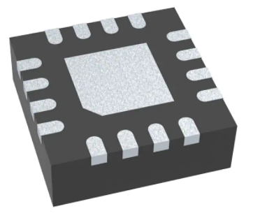
Available in 3 mm × 3 mm 16-pin QFN Package
The output voltage start-up ramp is controlled by the
SS pin, which allows operation as either a standalone
power supply or in tracking configurations. Power
sequencing is also possible by configuring the enable
and power good pins. In power save mode, the
devices operate at typically 20-µA quiescent current.
Power save mode is entered automatically and
seamlessly maintaining high efficiency over the entire
load current range.
Device Information(1)
PART NUMBER
PACKAGE
BODY SIZE (NOM)
2 Applications
TPS62090Q
•
•
•
•
(1) For all available packages, see the orderable addendum at
the end of the data sheet.
Automotive Applications
Distributed Power Supplies
Processor Supply
Battery-Powered Applications
SPACER
Typical Application
QFN (16)
Efficiency
TPS62090Q
VIN
2.5 V to 6 V
VOUT
1.8 V / 3.0 A
L1
470 nH
C3
10 nF
C4
10 nF
100
95
SW
PVIN
SW
AVIN
VOS
EN
FB
CP
PG
CN
FREQ
C2
22 µF
R3
500 k
90
R1
200 k
VOUT
R2
160 k
Efficiency (%)
PVIN
C1
10 µF
85
80
75
70
65
60
SS
AGND
3.00 mm × 3.00 mm
VPG
PGND PGND
55
50
100m
VIN = 2.7 V
VIN = 3.7 V
VIN = 4.2 V
VIN = 5 V
VOUT = 1.8 V
L = 0.4 µH
f = 2.8 MHz
1
10
100
I load (mA)
1k
10k
G004
Copyright © 2016, Texas Instruments Incorporated
1
An IMPORTANT NOTICE at the end of this data sheet addresses availability, warranty, changes, use in safety-critical applications,
intellectual property matters and other important disclaimers. PRODUCTION DATA.
�TPS62090-Q1
SLVSC55B – AUGUST 2013 – REVISED DECEMBER 2016
www.ti.com
Table of Contents
1
2
3
4
5
6
7
Features ..................................................................
Applications ...........................................................
Description .............................................................
Revision History.....................................................
Pin Configuration and Functions .........................
Specifications.........................................................
1
1
1
2
3
4
6.1
6.2
6.3
6.4
6.5
6.6
4
4
4
4
5
6
Absolute Maximum Ratings ......................................
ESD Ratings..............................................................
Recommended Operating Conditions.......................
Thermal Information ..................................................
Electrical Characteristics...........................................
Typical Characteristics ..............................................
Detailed Description .............................................. 8
7.1
7.2
7.3
7.4
Overview ................................................................... 8
Functional Block Diagram ......................................... 8
Feature Description................................................... 9
Device Functional Modes........................................ 11
8
Application and Implementation ........................ 13
8.1 Application Information............................................ 13
8.2 Typical Application .................................................. 13
8.3 System Examples ................................................... 19
9 Power Supply Recommendations...................... 20
10 Layout................................................................... 21
10.1 Layout Guidelines ................................................. 21
10.2 Layout Example .................................................... 21
11 Device and Documentation Support ................. 22
11.1
11.2
11.3
11.4
11.5
11.6
11.7
Device Support......................................................
Documentation Support ........................................
Receiving Notification of Documentation Updates
Community Resource............................................
Trademarks ...........................................................
Electrostatic Discharge Caution ............................
Glossary ................................................................
22
22
22
22
22
22
22
12 Mechanical, Packaging, and Orderable
Information ........................................................... 23
4 Revision History
NOTE: Page numbers for previous revisions may differ from page numbers in the current version.
Changes from Revision A (August 2013) to Revision B
Page
•
Added Pin Configuration and Functions section, ESD Ratings table, Feature Description section, Device Functional
Modes, Application and Implementation section, Power Supply Recommendations section, Layout section, Device
and Documentation Support section, and Mechanical, Packaging, and Orderable Information section ............................... 1
•
Updated FB pin description .................................................................................................................................................... 3
•
Added CN and CP pin voltage ............................................................................................................................................... 4
•
Added typical value of VH and VL .......................................................................................................................................... 5
•
Added new graphs to the Typical Characteristics section ..................................................................................................... 6
•
Added Switching frequency curves for VOUT = 1 V and VOUT = 3.3 V ............................................................................... 6
•
Added Enable and Disable (EN) section ................................................................................................................................ 9
•
Added Hiccup current limit during startup ............................................................................................................................. 9
•
Added Charge Pump (CP, CN) section................................................................................................................................ 11
•
Updated Input and Output Capacitor Selection section ....................................................................................................... 15
•
Moved graphs from Typical Characteristics to Application Curves section ......................................................................... 16
•
Updated TPS62090Q Layout ............................................................................................................................................... 21
2
Submit Documentation Feedback
Copyright © 2013–2016, Texas Instruments Incorporated
Product Folder Links: TPS62090-Q1
�TPS62090-Q1
www.ti.com
SLVSC55B – AUGUST 2013 – REVISED DECEMBER 2016
5 Pin Configuration and Functions
PG
4
EN
14
13
12
11
Exposed
Thermal Pad*
10
5
6
7
8
CN
3
PGND
FREQ
15
CP
2
PGND
SW
16
AGND
1
FB
SW
VOS
RGT Package
16-Pin QFN With Exposed Thermal Pad
Top View
9
PVIN
PVIN
AVIN
SS
The exposed thermal pad is connected to AGND.
Pin Functions
PIN
I/O
DESCRIPTION
NAME
NO.
AGND
6
AVIN
10
I
CN
8
I/O
Internal charge-pump flying capacitor. Connect a 10-nF capacitor between CP and CN.
CP
7
I/O
Internal charge-pump flying capacitor. Connect a 10-nF capacitor between CP and CN.
EN
13
I
Exposed
Thermal
Pad
—
—
FB
5
I
Feedback pin of the device.
For the adjustable version, connect a resistor divider to set the output voltage.
FREQ
3
I
This pin selects the switching frequency of the device. FREQ = Low sets the typical switching frequency to
2.8 MHz. FREQ = High sets the typical switching frequency to 1.4 MHz. This pin has an active pulldown
resistor of typically 400 kΩ and can be left floating for 2.8-MHz operation.
PG
4
O
Power good open-drain output. This pin is high impedance if the output voltage is within regulation. This pin
is pulled low if the output is below its nominal value. The pullup resistor can not be connected to any
voltage higher than the input voltage of the device.
PGND
14, 15
—
Power ground connection.
PVIN
11, 12
I
Power supply input voltage pin.
SS
9
I
Soft-start control pin. A capacitor is connected to this pin and sets the soft-start time. Leaving this pin
floating sets the minimum start-up time.
SW
1, 2
I/O
VOS
16
I
—
Analog ground.
Bias supply input voltage pin.
Device enable. To enable the device this pin needs to be pulled high. Pulling this pin low disables the
device. This pin has a pulldown resistor of typically 400 kΩ, which is active when EN is low.
The exposed thermal pad is connected to AGND. It must be soldered for mechanical reliability.
Switch pin of the power stage.
Output voltage sense pin. This pin needs to be connected to the output voltage.
Submit Documentation Feedback
Copyright © 2013–2016, Texas Instruments Incorporated
Product Folder Links: TPS62090-Q1
3
�TPS62090-Q1
SLVSC55B – AUGUST 2013 – REVISED DECEMBER 2016
www.ti.com
6 Specifications
6.1 Absolute Maximum Ratings
over operating free-air temperature range (unless otherwise noted) (1)
Voltage (2)
MIN
MAX
PVIN, AVIN, FB, SS, EN, FREQ, VOS
–0.3
7
SW, PG
–0.3
VIN + 0.3
CN, CP
-0.3
VIN + 7
Power Good sink current, PG
UNIT
V
1
mA
Operating junction temperature, TJ
–40
150
°C
Storage temperature, Tstg
–65
150
°C
(1)
(2)
Stresses beyond those listed under Absolute Maximum Ratings may cause permanent damage to the device. These are stress ratings
only, which do not imply functional operation of the device at these or any other conditions beyond those indicated under Recommended
Operating Conditions. Exposure to absolute-maximum-rated conditions for extended periods may affect device reliability.
All voltage values are with respect to network ground terminal.
6.2 ESD Ratings
VALUE
V(ESD)
(1)
Electrostatic discharge
Human-body model (HBM), per AEC Q100-002 (1)
±2500
Charged-device model (CDM), per AEC Q100-011
±1500
UNIT
V
AEC Q100-002 indicates that HBM stressing shall be in accordance with the ANSI/ESDA/JEDEC JS-001 specification.
6.3 Recommended Operating Conditions
For additional information, see Application Information.
MIN
MAX
UNIT
VIN
Input voltage
2.5
6
V
TJ
Operating junction temperature
–40
125
°C
6.4 Thermal Information
TPS62090-Q1
THERMAL METRIC (1)
RGT (QFN)
UNIT
16 PINS
RθJA
Junction-to-ambient thermal resistance
45.6
°C/W
RθJC(top)
Junction-to-case (top) thermal resistance
58.9
°C/W
RθJB
Junction-to-board thermal resistance
19
°C/W
ψJT
Junction-to-top characterization parameter
1.1
°C/W
ψJB
Junction-to-board characterization parameter
19
°C/W
RθJC(bot)
Junction-to-case (bottom) thermal resistance
4
°C/W
(1)
4
For more information about traditional and new thermal metrics, see the Semiconductor and IC Package Thermal Metrics application
report.
Submit Documentation Feedback
Copyright © 2013–2016, Texas Instruments Incorporated
Product Folder Links: TPS62090-Q1
�TPS62090-Q1
www.ti.com
SLVSC55B – AUGUST 2013 – REVISED DECEMBER 2016
6.5 Electrical Characteristics
VIN = 3.6 V, TJ = –40°C to 125°C, typical values are at TJ = 25°C (unless otherwise noted)
PARAMETER
TEST CONDITIONS
MIN
TYP
MAX
UNIT
SUPPLY
VIN
Input voltage range
IQIN
Quiescent current
Not switching, FB = FB +5 %, Into PVIN and AVIN
Isd
Shutdown current
Into PVIN and AVIN
Undervoltage lockout threshold
VIN falling
UVLO
2.5
2.1
Undervoltage lockout hysteresis
Thermal shutdown
6
20
Temperature rising
Thermal shutdown hysteresis
V
µA
0.6
5
2.2
2.3
µA
V
200
mV
150
ºC
20
ºC
0.65
V
CONTROL SIGNALS EN, FREQ
VH
High level input voltage
VIN = 2.5 to 6 V
1
VL
Low level input voltage
VIN = 2.5 to 6 V
0.6
0.4
V
Ilkg
Input leakage current
EN, FREQ = GND or VIN
10
100
nA
RPD
Pulldown resistance
400
kΩ
SOFT START
ISS
Soft-start current
6.3
7.5
8.7
µA
POWER GOOD
Vth
Power good threshold
VL
Low level voltage
IPG
PG sinking current
Ilkg
Leakage current
Output voltage rising
95%
Output voltage falling
90%
I(sink) = 1 mA
0.4
VPG = 3.6 V
10
V
1
mA
200
nA
POWER SWITCH
RDS(o
High-side FET on-resistance
ISW = 500 mA
50
n)
Low-side FET on-resistance
ISW = 500 mA
40
ILIM
High-side FET switch current limit
fs
Switching frequency
3.7
4.6
mΩ
mΩ
5.5
A
FREQ = GND, IOUT = 3 A
2.8
MHz
FREQ = VIN, IOUT = 3 A
1.4
MHz
OUTPUT
Vs
Output voltage
Rod
Output discharge resistor
VFB
Feedback regulation voltage
Feedback voltage
accuracy (1) (2)
VFB
IFB
VOUT
(1)
(2)
0.8
EN = GND, VOUT = 1.8 V
VIN
200
0.8
VIN ≥ VOUT + 1 V
V
IOUT = 1 A, PWM mode
–1.4%
1.4%
IOUT = 0 mA, FREQ = 2.8 MHz, VOUT
≥ 0.8 V, PFM mode
–1.4%
3%
IOUT = 0 mA, FREQ = 1.4 MHz, VOUT
≥ 1.2 V, PFM mode
–1.4%
3%
IOUT = 0 mA, FREQ = 1.4 MHz, VOUT
< 1.2 V, PFM mode
–1.4%
3.7%
IOUT = 1 A, PWM mode
–1.4%
1.4%
IOUT = 0 mA, FREQ = high and low,
PFM mode
–1.4%
2.5%
10
V
Ω
Feedback input bias current
VFB = 0.8 V
Output voltage accuracy (2)
VIN ≥ VOUT + 1 V, fixed output
voltage, f = 2.8 MHz, L = 0.47
µH, COUT = 22 µF or f = 1.4
MHz, L = 1 µH, COUT = 22 µF
100
nA
Line regulation
VOUT = 1.8 V, PWM operation
0.016%
V
Load regulation
VOUT = 1.8 V, PWM operation
0.04%
A
For output voltages < 1.2 V, use a 2 × 22 µF output capacitance to achieve 3% output voltage accuracy.
For more information, see Power Save Mode Operation.
Submit Documentation Feedback
Copyright © 2013–2016, Texas Instruments Incorporated
Product Folder Links: TPS62090-Q1
5
�TPS62090-Q1
SLVSC55B – AUGUST 2013 – REVISED DECEMBER 2016
www.ti.com
6.6 Typical Characteristics
70
25
60
Current (µA)
Resistance (Ω)
20
50
40
30
15
10
VOUT = 1.8 V
L = 1 µH
f = 1.4 MHz
20
TA = 85°C
TA = 25°C
TA = −40°C
10
0
2
2.5
3
3.5
4
4.5
5
Input Voltage (V)
5.5
6
5
0
6.5
2
Figure 1. High-Side FET ON-Resistance vs Input Voltage
3.5
4
4.5
Voltage (V)
5
1500
1000
500
VIN = 2.8 V
VIN = 3.3 V
VIN = 5.0 V
0
0.0
0.5
1.0
VOUT = 1 V
6
6.5
G011
1.5
Load (A)
2.0
2.5
2500
2000
1500
1000
VIN = 2.8 V
VIN = 3.3 V
VIN = 5.0 V
500
0
0.0
3.0
0.5
1.0
D030
L = 1 µH
FREQ = High
VOUT = 1 V
Figure 3. Switching Frequency vs Load Current
1.5
Load (A)
2.0
2.5
3.0
D031
L = 0.4 µH
FREQ = Low
Figure 4. Switching Frequency vs Load Current
3000
2000
Switching Frequency (kHz)
2500
2000
1500
1000
1500
1000
500
VIN = 2.8 V
VIN = 3.3 V
VIN = 5.0 V
500
/
/
0
2.5
3.0
VOUT = 1 V
3.5
4.0
4.5
Input Voltage (V)
+ )5(4
+ )5(4
5.0
5.5
/RZ
+LJK
6.0
0
0.0
0.5
D032
IOUT = 1 A
VOUT = 1.8 V
Figure 5. Frequency vs Input Voltage
6
5.5
3000
Switching Frequency (kHz)
Switching Frequency (kHz)
3
Figure 2. Quiescent Current vs Input Voltage
2000
Switching Frequency (kHz)
2.5
G024
TA = 85 °C
TA = 25 °C
TA = −40 °C
Submit Documentation Feedback
1.0
1.5
Load (A)
2.0
L = 1 µH
2.5
3.0
D033
FREQ = High
Figure 6. Frequency vs Load Current
Copyright © 2013–2016, Texas Instruments Incorporated
Product Folder Links: TPS62090-Q1
�TPS62090-Q1
www.ti.com
SLVSC55B – AUGUST 2013 – REVISED DECEMBER 2016
3000
3000
2500
2500
Switching Frequency (kHz)
Switching Frequency (kHz)
Typical Characteristics (continued)
2000
1500
1000
VIN = 2.8 V
VIN = 3.3 V
VIN = 5.0 V
500
0
0.0
0.5
1.0
VOUT = 1.8 V
1.5
Load (A)
2.0
2.5
2000
1500
1000
500
/
/
0
2.5
3.0
3.0
4.0
4.5
Input Voltage (V)
D034
L = 0.4 µH
FREQ = Low
VOUT = 1.8 V
Figure 7. Frequency vs Load Current
5.0
/RZ
+LJK
5.5
6.0
D035
IOUT = 1 A
Figure 8. Frequency vs Input Voltage
2000
3000
Switching Frequency (kHz)
Switching Frequency (kHz)
3.5
+ )5(4
+ )5(4
1500
1000
500
2500
2000
1500
1000
500
VIN = 5.0 V
0
0.0
0.5
VOUT = 3.3 V
1.0
1.5
Load (A)
2.0
2.5
VIN = 5.0 V
0
0.0
3.0
0.5
1.0
D036
L = 1 µH
FREQ = High
VOUT = 3.3 V
Figure 9. Frequency vs Load Current
1.5
Load (A)
2.0
L = 0.4 µH
2.5
3.0
D037
FREQ = Low
Figure 10. Frequency vs Load Current
3500
Switching Frequency (kHz)
3000
2500
2000
1500
1000
500
0
3.5
VOUT = 3.3 V
/
/
4.0
4.5
5.0
Input Voltage (V)
+ )5(4
+ )5(4
5.5
/RZ
+LJK
6.0
D038
IOUT = 1 A
Figure 11. Frequency vs Input Voltage
Submit Documentation Feedback
Copyright © 2013–2016, Texas Instruments Incorporated
Product Folder Links: TPS62090-Q1
7
�TPS62090-Q1
SLVSC55B – AUGUST 2013 – REVISED DECEMBER 2016
www.ti.com
7 Detailed Description
7.1 Overview
The TPS62090Q synchronous switched mode converter is based on DCS-Control (Direct Control with Seamless
transition into power save mode). DCS-Control is an advanced regulation topology that combines the advantages
of hysteretic and voltage mode control.
The DCS-Control topology operates in Pulse Width Modulation (PWM) mode for medium to heavy load
conditions and in power save mode at light load currents. In PWM, the converter operates with nominal switching
frequency of 2.8 MHz or 1.4 MHz, having a controlled frequency variation over the input voltage range. As the
load current decreases, the converter enters power save mode, reducing the switching frequency and minimizing
the IC quiescent current to achieve high efficiency over the entire load current range. DCS-Control supports both
operation modes (PWM and PFM) using a single building block with a seamless transition from PWM to power
save mode without effecting the output voltage. The TPS62090Q device offers excellent DC-voltage regulation
and load transient regulation, combined with low output voltage ripple, to minimize interference with RF circuits.
7.2 Functional Block Diagram
PG
CP
PVIN
CN
Charge Pump
for
Gate driver
VFB
Hiccup
current limit
#32 counter
VREF
High Side
Current
Sense
Bandgap
Undervoltage
Lockout
Thermal shutdown
AVIN
PVIN
EN
M1
400kΩ(2)
SW
MOSFET Driver
Anti Shoot Through
Converter Control
Logic
AGND
SW
High =1.4 MHz
Low = 2.8 MHz
FREQ
M2
400kΩ(2)
PGND
PGND
Comparator
ramp
Timer
ton
Direct Control
and
Compensation
VOS
R1
Error Amplifier
(1)
Adjustable
only
Vref
0.8V
R2
(1)
FB
(1)
R3
400kΩ
Vin
DCS - Control™
200Ω
Iss
Voltage clamp
Vref
SS
÷1.56
EN
Output voltage
discharge
logic
M3
Copyright © 2016, Texas Instruments Incorporated
(2) The resistors are disconnected when the pins are high.
8
Submit Documentation Feedback
Copyright © 2013–2016, Texas Instruments Incorporated
Product Folder Links: TPS62090-Q1
�TPS62090-Q1
www.ti.com
SLVSC55B – AUGUST 2013 – REVISED DECEMBER 2016
7.3 Feature Description
7.3.1 Enable and Disable (EN)
The device is enabled by setting the EN pin to a logic high. Accordingly, shutdown mode is forced if the EN pin is
pulled low with a shutdown current of typically 0.6 µA. In shutdown mode, the internal power switches as well as
the entire control circuitry are turned off. An internal resistor of 200 Ω discharges the output through the VOS pin
smoothly. An internal pulldown resistor of 400 kΩ is connected to the EN pin when the EN pin is low. The
pulldown resistor is disconnected when the EN pin is high.
7.3.2 Soft Start (SS) and Hiccup Current Limit During Start-Up
To minimize inrush current during start-up, the device has an adjustable soft start depending on the capacitor
value connected to the SS pin. The device charges the soft-start capacitor with a constant current of typically
7.5 µA. The feedback voltage follows this voltage with a fraction of 1.56 until the internal reference voltage of 0.8
V is reached. The soft-start operation is complete when the voltage at the soft-start capacitor has reached
typically 1.25 V. The soft-start time is calculated using Equation 1. The larger the soft-start capacitor, the longer
the soft-start time. The relation between soft-start voltage and feedback voltage is estimated using Equation 2.
1.25V
tSS = CSS x
7.5μA
(1)
VFB =
VSS
1.56
(2)
During start-up, the switch current limit is reduced to 1/3 (approximately 1.5 A) of its typical current limit of 4.6 A.
Once the output voltage exceeds typically 0.6 V, the current limit is released to its nominal value. The device
provides a reduced load current of approximately 1.5 A when the output voltage is below typically 0.6 V. Due to
this, a small or no soft-start time may trigger the short-circuit protection during start-up especially for larger output
capacitors. This is avoided by using a larger soft-start capacitance to extend the soft-start time. See Short-Circuit
Protection (Hiccup Mode) for details of the reduced current limit during start-up. Leaving the soft-start pin floating
sets the minimum start-up time (around 50 µs).
7.3.3 Voltage Tracking (SS)
The SS pin is externally driven by another voltage source to achieve output voltage tracking. The application
circuit is shown in Figure 12. The internal reference voltage follows the voltage at the SS pin with a fraction of
1.56 until the internal reference voltage of 0.8 V is reached. The device achieves ratiometric or coincidental
(simultaneous) output tracking, as shown in Figure 13.
VOUT1
VOUT2
R3
R1
SS
FB
R4
R2
GND
GND
Figure 12. Output Voltage Tracking
Submit Documentation Feedback
Copyright © 2013–2016, Texas Instruments Incorporated
Product Folder Links: TPS62090-Q1
9
�TPS62090-Q1
SLVSC55B – AUGUST 2013 – REVISED DECEMBER 2016
www.ti.com
Feature Description (continued)
Voltage
Voltage
1+
VOUT1
VOUT1
VOUT2
VOUT2
R3 æ
R1 ö
1
< ç1 +
÷´
R 4 è R 2 ø 1.56
1+
R3 æ
R1 ö
1
= ç1 +
÷´
R 4 è R 2 ø 1.56
t
t
a) Ratiometric Tracking
b) Coincidental Tracking
Figure 13. Voltage Tracking Options
The R2 value should be set properly to achieve accurate voltage tracking by taking 7.5-µA soft start-up current
into account. 1 kΩ or smaller is a sufficient value for R2.
For decreasing the SS pin voltage, the device does not sink current from the output when the device is in power
save mode. So the resulting decreases of the output voltage may be slower than the SS pin voltage if the load is
light. When driving the SS pin with an external voltage, do not exceed the voltage rating of the SS pin which is
7 V.
7.3.4 Short-Circuit Protection (Hiccup Mode)
The device is protected against hard short circuits to GND and overcurrent events. This protection is
implemented by a two-level short-circuit protection. During start-up and when the output is shorted to GND, the
switch current limit is reduced to 1/3 of the typical current limit of 4.6 A. When the output voltage exceeds
typically 0.6 V, the current limit is released to the nominal value. The full current limit is implemented as a hiccup
current limit. Once the internal current limits are triggered 32 times, the device stops switching and starts a new
start-up sequence after a typical delay time of 66 µS passed by. The device continues in this cycle until the high
current condition is released.
7.3.5 Output Discharge Function
To ensure the device starts up under the defined conditions, the output discharges through the VOS pin with a
typical discharge resistor of 200 Ω whenever the device shuts down. This discharge happens when the device is
disabled or if thermal shutdown, undervoltage lockout or short-circuit hiccup mode is triggered.
7.3.6 Power Good Output (PG)
The power good output is low when the output voltage is below the nominal value. The power good becomes
high impedance once the output is within 5% of regulation. The PG pin is an open-drain output and is specified
to typically sink up to 1 mA. This output requires a pullup resistor to be monitored properly. The pullup resistor
cannot be connected to any voltage higher than the input voltage of the device. The PG output is low when the
device is disabled, in thermal shutdown, or in UVLO. The PG output can be left floating if unused.
10
Submit Documentation Feedback
Copyright © 2013–2016, Texas Instruments Incorporated
Product Folder Links: TPS62090-Q1
�TPS62090-Q1
www.ti.com
SLVSC55B – AUGUST 2013 – REVISED DECEMBER 2016
Feature Description (continued)
7.3.7 Frequency Set Pin (FREQ)
The FREQ pin is a digital logic input which sets the nominal switching frequency. Pulling this pin to GND sets the
nominal switching frequency to 2.8 MHz and pulling this pin high sets the nominal switching frequency to
1.4 MHz. Because this pin changes the switching frequency, it also changes the on-time during PFM mode. At
1.4 MHz the on-time is twice the on-time as operating at 2.8 MHz. This pin has an active pulldown resistor of
typically 400 kΩ. For applications where efficiency is of highest importance, a lower switching frequency should
be selected. A higher switching frequency allows the use of smaller external components, faster load transient
response, and lower output voltage ripple when using same L-C values.
7.3.8 Undervoltage Lockout (UVLO)
To avoid mis-operation of the device at low input voltages, an undervoltage lockout is included. UVLO shuts
down the device at input voltages lower than typically 2.2 V with a 200-mV hysteresis.
7.3.9 Thermal Shutdown
The device enters thermal shutdown once the junction temperature exceeds typically 150°C with a 20°C
hysteresis.
7.3.10 Charge Pump (CP, CN)
The CP and CN pins must attach to an external 10-nF capacitor to complete a charge pump for the gate driver.
This capacitor must be rated for the input voltage. TI does not recommend connecting any other circuits to the
CP or CN pins.
7.4 Device Functional Modes
7.4.1 Pulse Width Modulation Operation
At medium to heavy load currents, the device operates with PWM at a nominal switching frequency of 2.8 MHz
or 1.4 MHz depending on the setting of the FREQ pin. As the load current decreases, the converter enters the
power save mode operation reducing the switching frequency. The device enters power save mode at the
boundary to discontinuous conduction mode (DCM).
7.4.2 Power Save Mode Operation
As the load current decreases, the converter enters power save mode operation. During power save mode, the
converter operates with reduced switching frequency in PFM mode and with a minimum quiescent current while
maintaining high efficiency. The power save mode is based on a fixed on-time architecture following Equation 3.
When operating at 1.4 MHz, the on-time is twice as long as the on-time for 2.8-MHz operation, resulting in larger
output voltage ripple, as shown in Figure 24 and Figure 25, and slightly higher output voltage at no load, as
shown in Figure 21 and Figure 22. To have the same output voltage ripple at 1.4 MHz during PFM mode, either
the output capacitor or the inductor value must be increased. As an example, operating at 2.8 MHz using
0.47-µH inductor gives the same output voltage ripple as operating with 1.4 MHz using 1-µH inductor.
V
OUT × 360ns
V
IN
V
OUT
ton1.4MHz =
× 360ns × 2
V
IN
2×I
OUT
f =
æ
ö V -V
V
V
OUT ÷ x IN
OUT
ton2 ç 1 + IN
ç
÷
V
L
OUT
è
ø
ton2.8MHz =
(3)
In power save mode the output voltage rises slightly above the nominal output voltage in PWM mode, as shown
in Figure 21 and Figure 22. This effect is reduced by increasing the output capacitance or the inductor value.
This effect is also reduced by programming the output voltage of the TPS62090Q lower than the target value. As
an example, if the target output voltage is 3.3 V, then the TPS62090Q is programmed to 3.3 V – 0.8%. As a
result the output voltage accuracy is now –2.2% to +2.2% instead of –1.4% to 3%. The output voltage accuracy
in PFM operation is reflected in the Electrical Characteristics table and given for a 22-µF output capacitance.
Submit Documentation Feedback
Copyright © 2013–2016, Texas Instruments Incorporated
Product Folder Links: TPS62090-Q1
11
�TPS62090-Q1
SLVSC55B – AUGUST 2013 – REVISED DECEMBER 2016
www.ti.com
Device Functional Modes (continued)
7.4.3 Low-Dropout Operation (100% Duty Cycle)
The device offers low input to output voltage difference by entering 100% duty cycle mode. In this mode the highside MOSFET switch is constantly turned on which is particularly useful in battery-powered applications to
achieve longest operation time by taking full advantage of the whole battery voltage range. The minimum input
voltage where the output voltage falls below the nominal regulation value is given by Equation 4.
VIN(min) = VOUT + IOUT × ( RDS(on) + RL )
Where
•
•
12
RDS(on) = High side FET on-resistance
RL = DC resistance of the inductor
Submit Documentation Feedback
(4)
Copyright © 2013–2016, Texas Instruments Incorporated
Product Folder Links: TPS62090-Q1
�TPS62090-Q1
www.ti.com
SLVSC55B – AUGUST 2013 – REVISED DECEMBER 2016
8 Application and Implementation
NOTE
Information in the following applications sections is not part of the TI component
specification, and TI does not warrant its accuracy or completeness. TI’s customers are
responsible for determining suitability of components for their purposes. Customers should
validate and test their design implementation to confirm system functionality.
8.1 Application Information
The TPS62090-Q1 device is a high-frequency, synchronous, step-down converter optimized for small solution
size, high efficiency, and is suitable for battery-powered applications.
8.2 Typical Application
TPS62090Q
VIN
2.5 V to 6 V
VOUT
1.8 V / 3.0 A
L1
470 nH
C1
10 µF
C3
10 nF
C4
10 nF
PVIN
SW
PVIN
SW
AVIN
VOS
EN
FB
CP
PG
CN
FREQ
SS
AGND
C2
22 µF
R3
500 k
R1
200 k
VOUT
R2
160 k
VPG
PGND PGND
Copyright © 2016, Texas Instruments Incorporated
Figure 14. Test Circuit
8.2.1 Design Requirements
Table 1 is a recommended list of components for the test circuit in Figure 14.
Table 1. List of Components
REFERENCE
DESCRIPTION
MANUFACTURER
TPS62090Q
High efficiency step-down converter
Texas Instruments
L1
Inductor: 1 µH, 0.47 µH, 0.4 µH
Coilcraft XFL4020-102, XAL4020-401, TOKO DEF252012-R47
C1
Ceramic capacitor: 10 µF, 22 µF
(6.3-V, X5R, 0603), (6.3-V, X5R, 0805)
C2
Ceramic capacitor: 22 µF
(6.3-V, X5R, 0805)
C3, C4
Ceramic capacitor
Standard
R1, R2, R3
Resistor
Standard
Submit Documentation Feedback
Copyright © 2013–2016, Texas Instruments Incorporated
Product Folder Links: TPS62090-Q1
13
�TPS62090-Q1
SLVSC55B – AUGUST 2013 – REVISED DECEMBER 2016
www.ti.com
8.2.2 Detailed Design Procedure
The first step in the design procedure is the selection of the output filter components. To simplify this process,
Table 2 and Table 3 list possible inductor and capacitor value combinations.
Table 2. Output Filter Selection (2.8-MHz Operation, FREQ = GND)
INDUCTOR VALUE (µH) (1)
(1)
(2)
(3)
OUTPUT CAPACITOR VALUE (µF) (2)
10
22
47
100
150
0.47
—
√ (3)
√
√
√
1
√
√
√
√
√
2.2
—
—
—
—
—
3.3
—
—
—
—
—
Inductor tolerance and current de-rating is anticipated. The effective inductance varies by +20% and
–30%.
Capacitance tolerance and bias voltage de-rating is anticipated. The effective capacitance varies by
+20% and –50%.
Typical application configuration. Other check marks indicate alternative filter combinations.
Table 3. Output Filter Selection (1.4-MHz Operation, FREQ = VIN)
INDUCTOR VALUE (µH) (1)
(1)
(2)
(3)
OUTPUT CAPACITOR VALUE (µF) (2)
10
22
47
100
150
0.47
—
√
√
√
√
1
√
√ (3)
√
√
√
2.2
√
√
√
√
√
3.3
—
—
—
—
—
Inductor tolerance and current de-rating is anticipated. The effective inductance varies by +20% and
–30%.
Capacitance tolerance and bias voltage de-rating is anticipated. The effective capacitance varies by
+20% and –50%.
Typical application configuration. Other check marks indicate alternative filter combinations.
8.2.2.1 Inductor Selection
The inductor selection is affected by several parameters such as inductor-ripple current, output-voltage ripple,
transition point into power save mode, and efficiency. See Table 4 for typical inductors.
Table 4. Inductor Selection
INDUCTOR VALUE
COMPONENT SUPPLIER
SIZE (L × W × H mm)
Isat / DCR
0.6 µH
Coilcraft XAL4012-601
4 × 4 × 2.1
7.1 A / 9.5 mΩ
1 µH
Coilcraft XAL4020-102
4 × 4 × 2.1
5.9 A / 13.2 mΩ
1 µH
Coilcraft XFL4020-102
4 × 4 × 2.1
5.1 A / 10.8 mΩ
0.47 µH
TOKO DFE252012 R47
2.5 × 2 × 1.2
3.7 A / 39 mΩ
1 µH
TOKO DFE252012 1R0
2.5 × 2 × 1.2
3.0 A / 59 mΩ
0.68 µH
TOKO DFE322512 R68
3.2 × 2.5 × 1.2
3.5 A / 37 mΩ
1 µH
TOKO DFE322512 1R0
3.2 × 2.5 × 1.2
3.1 A / 45 mΩ
In addition, the inductor must be rated for the appropriate saturation current and DC resistance (DCR). The
inductor must be rated for a saturation current as high as the typical switch current limit, of 4.6 A or according to
Equation 5 and Equation 6. Equation 5 and Equation 6 calculate the maximum inductor current under static load
conditions. The formula takes the converter efficiency into account. The converter efficiency is taken from the
Typical Characteristics graphs or 80% can be used as a conservative approach. The calculation must be done
for the maximum input voltage where the peak switch current is highest.
I =I
+
L
OUT
14
ΔI
L
2
(5)
Submit Documentation Feedback
Copyright © 2013–2016, Texas Instruments Incorporated
Product Folder Links: TPS62090-Q1
�TPS62090-Q1
www.ti.com
SLVSC55B – AUGUST 2013 – REVISED DECEMBER 2016
æ
ö
V
V
OUT x ç 1 - OUT ÷
ç
η
V x η÷
IN
è
ø
I =I
+
L
OUT
2x f xL
where
•
•
•
ƒ = Converter switching frequency (typical 2.8 MHz or 1.4 MHz)
L = Selected inductor value
η = Estimated converter efficiency (use the number from the efficiency curves or 0.80 as an conservative
assumption)
(6)
NOTE
The calculation must be done for the maximum input voltage of the application
Calculating the maximum inductor current using the actual operating conditions gives the minimum saturation
current. A margin of 20% must be added to cover for load transients during operation.
8.2.2.2 Input and Output Capacitor Selection
For best output and input voltage filtering, low-ESR (X5R or X7R) ceramic capacitors are recommended. The
input capacitor minimizes input voltage ripple, suppresses input voltage spikes and provides a stable system rail
for the device. A 10-µF or larger input capacitor is recommended when FREQ = Low and a 22-µF or larger when
FREQ = High.
The output capacitor value can range from 10 µF up to 150 µF and beyond. Load transient testing and
measuring the bode plot are good ways to verify stability with larger capacitor values. The recommended typical
output capacitor value is 22 µF (nominal) and can vary over a wide range as outline in the output filter selection
table. For output voltages above 1.8 V, noise can cause duty cycle jitter. This does not degrade device
performance. Using an output capacitor of 2 × 22 µF (nominal) for output voltages >1.8 V avoids duty cycle jitter.
Ceramic capacitor have a DC-Bias effect, which has a strong influence on the final effective capacitance. Choose
the right capacitor carefully in combination with considering its package size and voltage rating.
8.2.2.3 Setting the Output Voltage
The output voltage is set by an external resistor divider according to Equation 7, Equation 8, and Equation 9.
R1 ö
R1 ö
æ
æ
VOUT = VFB ´ ç 1 +
= 0.8 V ´ ç 1 +
÷
R2 ø
R2 ÷ø
è
è
(7)
V
0.8 V
R2 = FB =
» 160 kΩ
IFB
5 μA
(8)
æV
ö
æV
ö
R1 = R2 ´ ç OUT - 1÷ = R2 ´ ç OUT - 1÷
V
0.8V
è
ø
è FB
ø
(9)
When sizing R2, use a minimum of 5 µA for the feedback current (IFB) to achieve low quiescent current and
acceptable noise sensitivity. Larger currents through R2 improve noise sensitivity and output voltage accuracy. A
feed-forward capacitor is not required for proper operation.
Submit Documentation Feedback
Copyright © 2013–2016, Texas Instruments Incorporated
Product Folder Links: TPS62090-Q1
15
�TPS62090-Q1
SLVSC55B – AUGUST 2013 – REVISED DECEMBER 2016
www.ti.com
100
100
95
95
90
90
85
85
Efficiency (%)
Efficiency (%)
8.2.3 Application Curves
80
75
70
65
60
55
50
100m
80
75
70
65
VOUT = 3.3 V
L = 1 µH
f = 1.4 MHz
1
VIN = 3.7 V
VIN = 4.2 V
VIN = 5 V
10
100
I load (mA)
1k
60
55
50
100m
10k
95
90
90
85
85
Efficiency (%)
Efficiency (%)
100
95
80
75
70
55
50
100m
1
10
100
I load (mA)
1k
60
55
50
100m
10k
90
85
85
Efficiency (%)
Efficiency (%)
95
80
75
70
1
10
100
I load (mA)
1k
10k
G004
75
70
65
VIN = 2.7 V
VIN = 3.7 V
VIN = 4.2 V
VIN = 5 V
1k
10
100
I load (mA)
80
60
55
10k
50
100m
G005
Figure 19. Efficiency vs Load Current
16
1
Figure 18. Efficiency vs Load Current
90
50
100m
VIN = 2.7 V
VIN = 3.7 V
VIN = 4.2 V
VIN = 5 V
VOUT = 1.8 V
L = 0.4 µH
f = 2.8 MHz
G003
100
55
G001
70
95
VOUT = 1.05 V
L = 1.0 µH
f = 1.4 MHz
10k
75
100
60
1k
80
Figure 17. Efficiency vs Load Current
65
10
100
I load (mA)
65
VIN = 2.7 V
VIN = 3.7 V
VIN = 4.2 V
VIN = 5 V
VOUT = 1.8 V
L = 1 µH
f = 1.4 MHz
VIN = 3.7 V
VIN = 4.2 V
VIN = 5 V
Figure 16. Efficiency vs Load Current
100
60
1
G002
Figure 15. Efficiency vs Load Current
65
VOUT = 3.3 V
L = 1 µH
f = 2.8 MHz
Submit Documentation Feedback
VOUT = 1.05 V
L = 0.4 µH
f = 2.8 MHz
1
10
100
I load (mA)
VIN = 2.7 V
VIN = 3.7 V
VIN = 4.2 V
VIN = 5 V
1k
10k
G006
Figure 20. Efficiency vs Load Current
Copyright © 2013–2016, Texas Instruments Incorporated
Product Folder Links: TPS62090-Q1
�TPS62090-Q1
www.ti.com
SLVSC55B – AUGUST 2013 – REVISED DECEMBER 2016
1.83
1.82
VIN = 5.0 V
VIN = 4.2 V
VIN = 3.7 V
1.825
Output Voltage (V)
Output Voltage (V)
1.825
1.83
VOUT = 1.8 V
L = 1 µH
f = 1.4 MHz
1.815
1.81
1.805
1.8
1.795
1.82
1.815
1.81
1.805
1.8
1
10
100
I load (mA)
1k
10k
1.79
100m
G007
Figure 21. Output Voltage vs Load Current
Vsw
2 V/div
Vo
20 mV/div
Vo
20 mV/div
Vin = 3.7 V
Vo=1.8 V/3 A
f = 1.4 MHz, L = 1 µH
400 ns/div
1
10
100
I load (mA)
1k
10k
G008
Figure 22. Output Voltage vs Load Current
Vsw
2 V/div
Iinductor
500 mA/div
Vin = 3.7 V
Vo = 1.8 V/100 mA
f = 1.4 MHz, L = 1 µH
1 µs/div
G012
Figure 23. PWM Operation
G013
Figure 24. PFM Operation
Vo
20 mV/div
Vsw
2 V/div
Io
1 A/div
Vo
20 mV/div
Iinductor
500 mA/div
VIN = 5.0 V
VIN = 4.2 V
VIN = 3.7 V
1.795
1.79
100m
Iinductor
1 A/div
VOUT = 1.8 V
L = 0.4 µH
f = 2.8 MHz
Vin = 3.7 V
Vo = 1.8 V/100 mA
f = 2.8 MHz, L = 0.47 µH
1 µs/div
Iinductor
500 mA/div
G014
Figure 25. PFM Operation
Vin = 3.7 V
Vo = 1.8 V
f = 1.4 MHz, L = 1 µH
200 µs/div
G015
Figure 26. Load Sweep
Submit Documentation Feedback
Copyright © 2013–2016, Texas Instruments Incorporated
Product Folder Links: TPS62090-Q1
17
�TPS62090-Q1
SLVSC55B – AUGUST 2013 – REVISED DECEMBER 2016
www.ti.com
Vo
20 mV/div
VEN
2 V/div
Vo
1 V/div
Io
2 A/div
Iinductor
500 mA/div
Vin = 3.7 V
Vo = 1.8 V
f = 2.8 MHz, L = 1 µH
Iinductor
500 mA/div
200 µs/div
G016
VO = 1.8 V / 600 mA
Figure 27. Load Sweep
VEN
2 V/div
Vo
1 V/div
Io
2 A/div
Iinductor
500 mA/div
Iinductor
1 A/div
2 ms/div
f = 1.4 MHz / L = 1 µH
Vin = 3.7 V
Vo = 1.8 V
f = 1.4 MHz, L = 1 µH
40 µs/div
G018
G019
Figure 30. Hiccup Short-Circuit Protection
Figure 29. Shutdown
Vo
1 V/div
Vo
50 mV/div
Io
2 A/div
Io
1 A/div
Vin = 3.7 V
Vo = 1.8 V
f = 1.4 MHz, L = 1 µH
Iinductor
1 A/div
Iinductor
1 A/div
400 µs/div
G020
Figure 31. Hiccup Short-Circuit Protection
18
G017
CSS = 10 nF
Figure 28. Start-Up
Vo
1 V/div
VO = 1.8 V / No Load
400 µs/div
f = 2.8 MHz / L = 1 µH
Submit Documentation Feedback
Vin = 3.7 V
Vo = 1.8 V,0.3 A to 2.5 A
f = 1.4 MHz, L = 1 µH
Co = 22 µF
4 µs/div
G021
Figure 32. Load Transient Response
Copyright © 2013–2016, Texas Instruments Incorporated
Product Folder Links: TPS62090-Q1
�TPS62090-Q1
www.ti.com
SLVSC55B – AUGUST 2013 – REVISED DECEMBER 2016
Vo
50 mV/div
Vo
50 mV/div
Io
1 V/div
Vin = 3.7 V
Vo = 1.8 V, 0.3 A to 2.5 A
f = 1.4 MHz, L = 1 µH
Co = 22 µF
Iinductor
1 A/div
Iinductor
500 A/div
40 µs/div
Vin = 3.7 V
Vo = 1.8 V, 20 mA to 1 A
f = 1.4 MHz, L = 1 µH
Co = 22 µF
100 µs/div
G022
Figure 33. Load Transient Response
G023
Figure 34. Load Transient Response
8.3 System Examples
Figure 35, Figure 36, and Figure 37 show additional circuits for varying voltage options.
TPS6209x-Q1
Vin
2.5 to 6 V
12
11
C1
10 mF
10
C3
10 nF
PVIN
SW
PVIN
SW
AVIN
VOS
13 EN
7
8
C4
10 nF
9 SS
Vout
1.5 V / 3 A
R1
140 k
2
C2
22 mF
16
R2
160 k
FB 5
R3
500 k
PG 4
CP
CN
1
L1
470 nH
FREQ
Power Good
3
AGND 6
PGND PGND
14
15
Copyright © 2016, Texas Instruments Incorporated
Figure 35. 1.5-V Adjustable Version Operating at 2.8 MHz
Submit Documentation Feedback
Copyright © 2013–2016, Texas Instruments Incorporated
Product Folder Links: TPS62090-Q1
19
�TPS62090-Q1
SLVSC55B – AUGUST 2013 – REVISED DECEMBER 2016
www.ti.com
System Examples (continued)
L1
1 mH
TPS6209x-Q1
Vin
2.5 to 6 V
12
C1
22 mF
11
10
C3
10 nF
SW
PVIN
SW
AVIN
VOS
7
9
Vout
1.8 V / 3 A
R1
200 k
2
C2
22 mF
16
R2
160 k
FB 5
13 EN
8
C4
10 nF
PVIN
1
R3
500 k
PG 4
CP
CN
FREQ
SS
AGND
3
Power Good
Vin
6
PGND PGND
14
15
Copyright © 2016, Texas Instruments Incorporated
Figure 36. 1.8-V Adjustable Version Operating at 1.4 MHz
TPS6209x-Q1
Vin
2.5 to 6 V
12
11
C1
22 mF
10
C3
10 nF
SW
PVIN
SW
AVIN
VOS
7
9
1
Vout
1.05 V / 3 A
R1
68 k
2
C2
22 mF
16
R2
220 k
FB 5
13 EN
8
C4
10 nF
PVIN
L1
1 mH
R3
500 k
PG 4
CP
CN
FREQ
SS
AGND
3
Power Good
Vin
6
PGND PGND
14
15
Copyright © 2016, Texas Instruments Incorporated
Figure 37. 1.05-V Adjustable Version Operating at 1.4 MHz
9 Power Supply Recommendations
The power supply to the TPS62090-Q1 device must have a current rating according to the supply voltage, output
voltage, and output current of the TPS62090-Q1 device.
20
Submit Documentation Feedback
Copyright © 2013–2016, Texas Instruments Incorporated
Product Folder Links: TPS62090-Q1
�TPS62090-Q1
www.ti.com
SLVSC55B – AUGUST 2013 – REVISED DECEMBER 2016
10 Layout
10.1 Layout Guidelines
•
•
•
•
•
TI recommends placing the input capacitor as close as possible to the IC pins PVIN and PGND.
The VOS connection is noise sensitive and needs to be routed as short and directly to the output pin of the
inductor.
The exposed thermal pad of the package, analog ground (pin 6) and power ground (pin 14, 15) should have a
single joint connection at the exposed thermal pad of the package. This minimizes switch node jitter.
The charge pump capacitor connected to CP and CN should be placed close to the IC to minimize coupling of
switching waveforms into other traces and circuits.
Refer to the TPS62090EVM-063 Evaluation Module (SLVU670) for an example of component placement,
routing, and thermal design.
R2x1
R1
AGND
R2
L1x1
10.2 Layout Example
L1
VOUT
C2
SW
PG
SW
FREQ
C5
EN
C4
PVIN
CN
SS
PGND
AVIN
VOS
PGND
CP
PVIN
FB
AGND
VIN
GND
C1
Figure 38. TPS62090Q Layout
Submit Documentation Feedback
Copyright © 2013–2016, Texas Instruments Incorporated
Product Folder Links: TPS62090-Q1
21
�TPS62090-Q1
SLVSC55B – AUGUST 2013 – REVISED DECEMBER 2016
www.ti.com
11 Device and Documentation Support
11.1 Device Support
11.1.1 Third-Party Products Disclaimer
TI'S PUBLICATION OF INFORMATION REGARDING THIRD-PARTY PRODUCTS OR SERVICES DOES NOT
CONSTITUTE AN ENDORSEMENT REGARDING THE SUITABILITY OF SUCH PRODUCTS OR SERVICES
OR A WARRANTY, REPRESENTATION OR ENDORSEMENT OF SUCH PRODUCTS OR SERVICES, EITHER
ALONE OR IN COMBINATION WITH ANY TI PRODUCT OR SERVICE.
11.2 Documentation Support
11.2.1 Related Documentation
For related documentation see the following:
• Basic Calculation of a Buck Converter's Power Stage (SLVA477)
• Choosing an Appropriate Pull-up/Pull-down Resistor for Open Drain Outputs (SLVA485)
• How to Measure the Control Loop of DCS-Control™ Devices (SLVA465)
• Optimizing the TPS62090 Output Filter (SLVA519)
• Performing Accurate PFM Mode Efficiency Measurements (SLVA236)
• QFN/SON PCB Attachment (SLUA271)
• TPS62090EVM-063 Evaluation Module (SLVU670)
• Understanding the Absolute Maximum Ratings of the SW Node (SLVA494)
11.3 Receiving Notification of Documentation Updates
To receive notification of documentation updates, navigate to the device product folder on ti.com. In the upper
right corner, click on Alert me to register and receive a weekly digest of any product information that has
changed. For change details, review the revision history included in any revised document.
11.4 Community Resource
The following links connect to TI community resources. Linked contents are provided "AS IS" by the respective
contributors. They do not constitute TI specifications and do not necessarily reflect TI's views; see TI's Terms of
Use.
TI E2E™ Online Community TI's Engineer-to-Engineer (E2E) Community. Created to foster collaboration
among engineers. At e2e.ti.com, you can ask questions, share knowledge, explore ideas and help
solve problems with fellow engineers.
Design Support TI's Design Support Quickly find helpful E2E forums along with design support tools and
contact information for technical support.
11.5 Trademarks
DCS-Control, E2E are trademarks of Texas Instruments.
All other trademarks are the property of their respective owners.
11.6 Electrostatic Discharge Caution
These devices have limited built-in ESD protection. The leads should be shorted together or the device placed in conductive foam
during storage or handling to prevent electrostatic damage to the MOS gates.
11.7 Glossary
SLYZ022 — TI Glossary.
This glossary lists and explains terms, acronyms, and definitions.
22
Submit Documentation Feedback
Copyright © 2013–2016, Texas Instruments Incorporated
Product Folder Links: TPS62090-Q1
�TPS62090-Q1
www.ti.com
SLVSC55B – AUGUST 2013 – REVISED DECEMBER 2016
12 Mechanical, Packaging, and Orderable Information
The following pages include mechanical, packaging, and orderable information. This information is the most
current data available for the designated devices. This data is subject to change without notice and revision of
this document. For browser-based versions of this data sheet, refer to the left-hand navigation.
Submit Documentation Feedback
Copyright © 2013–2016, Texas Instruments Incorporated
Product Folder Links: TPS62090-Q1
23
�PACKAGE OPTION ADDENDUM
www.ti.com
6-Feb-2020
PACKAGING INFORMATION
Orderable Device
Status
(1)
TPS62090QRGTRQ1
ACTIVE
Package Type Package Pins Package
Drawing
Qty
VQFN
RGT
16
3000
Eco Plan
Lead/Ball Finish
MSL Peak Temp
(2)
(6)
(3)
Green (RoHS
& no Sb/Br)
NIPDAU
Level-2-260C-1 YEAR
Op Temp (°C)
Device Marking
(4/5)
-40 to 125
SJG
(1)
The marketing status values are defined as follows:
ACTIVE: Product device recommended for new designs.
LIFEBUY: TI has announced that the device will be discontinued, and a lifetime-buy period is in effect.
NRND: Not recommended for new designs. Device is in production to support existing customers, but TI does not recommend using this part in a new design.
PREVIEW: Device has been announced but is not in production. Samples may or may not be available.
OBSOLETE: TI has discontinued the production of the device.
(2)
RoHS: TI defines "RoHS" to mean semiconductor products that are compliant with the current EU RoHS requirements for all 10 RoHS substances, including the requirement that RoHS substance
do not exceed 0.1% by weight in homogeneous materials. Where designed to be soldered at high temperatures, "RoHS" products are suitable for use in specified lead-free processes. TI may
reference these types of products as "Pb-Free".
RoHS Exempt: TI defines "RoHS Exempt" to mean products that contain lead but are compliant with EU RoHS pursuant to a specific EU RoHS exemption.
Green: TI defines "Green" to mean the content of Chlorine (Cl) and Bromine (Br) based flame retardants meet JS709B low halogen requirements of