Order
Now
Product
Folder
Support &
Community
Tools &
Software
Technical
Documents
TPS62097-Q1
SLVSDZ7A – SEPTEMBER 2017 – REVISED DECEMBER 2017
TPS62097-Q1 2-A High Efficiency Step-Down Converter in Wettable Flanks QFN Package
1 Features
3 Description
•
The TPS62097-Q1 device is a synchronous stepdown converter optimized for high efficiency and
noise critical applications. The devices focus on high
efficiency conversion over a wide output current
range. At medium to heavy loads, the converter
operates in PWM mode and automatically enters
Power Save Mode operation at light load. The
switching frequency is selectable in the range of 1.5
MHz to 2.5 MHz by an external resistor. iDCS-Control
is able to be operated in a forced PWM mode for low
noise operation with a constant switching frequency.
1
•
•
•
•
•
•
•
•
•
•
•
•
•
•
•
AEC-Q100 Qualified With the Following Results:
– Device Temperature Grade 1: –40°C to 125°C
Operating Junction Temperature Range
– Device HBM ESD Classification Level 2
– Device CDM ESD Classification Level C6
iDCS-Control Topology with Selectable Switching
Frequency
Forced PWM or Power Save Mode
Up to 97% Efficiency
2.5-V to 6.0-V Input Voltage
0.8-V to VIN Adjustable Output Voltage
3.3-V Fixed Output Voltage, TPS6209733-Q1
±1% Output Voltage Accuracy
Hiccup Short Circuit Protection
Programmable Soft Startup
Output Voltage Tracking
100% Duty Cycle for Lowest Dropout
Output Discharge
Power Good Output
Thermal Shutdown Protection
Available in 3-mm x 3-mm QFN Package with
Wettable Flanks
2 Applications
•
•
•
•
To address the requirements of system power rails,
the internal compensation circuit allows a large
selection of external output capacitor values in
excess of 150 µF. To control the inrush current during
the startup, the device provides a programmable soft
startup by an external capacitor connected to the
SS/TR pin. The SS/TR pin is also used in voltage
tracking configurations. The device integrates short
circuit protection, power good and thermal shutdown
features.
Device Information(1)
PART NUMBER
PACKAGE
BODY SIZE (NOM)
TPS62097-Q1
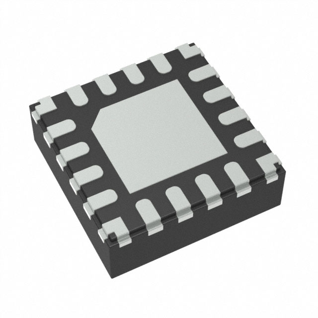
QFN (16)
3.0 mm x 3.0 mm
TPS6209733-Q1
QFN (16)
3.0 mm x 3.0 mm
(1) For all available packages, see the orderable addendum at
the end of the datasheet.
Output Voltage Options
Gateway
Head Unit
Instrumentation Cluster
Telematics
PART NUMBER
OUTPUT VOLTAGE
MARKING
SYMBOL
TPS62097-Q1
Adj.
9700Q
TPS6209733-Q1
3.3 V
9733Q
1.8-V Output, Typical Application
TPS62097-Q1
C1
10 µF
C3
10 nF
PVIN
SW
AVIN
VOS
L1
1.0 µH
C2
22 µF
EN
R4*
SS/TR
FB
MODE
PG
AGND
VPG
PGND
100
VOUT
1.8 V
R3
100 k
R1
24.9 k
R2
20 k
90
Efficiency (%)
VIN
5.0 V
1.8-V Output, Efficiency, MODE = Open
80
70
R4: optional
VIN
VIN = 3.3 V
VIN = 5.0 V
Copyright Ú 2016, Texas Instruments Incorporated
60
0
0.5
1
Load (A)
1.5
2
D026
1
An IMPORTANT NOTICE at the end of this data sheet addresses availability, warranty, changes, use in safety-critical applications,
intellectual property matters and other important disclaimers. PRODUCTION DATA.
�TPS62097-Q1
SLVSDZ7A – SEPTEMBER 2017 – REVISED DECEMBER 2017
www.ti.com
Table of Contents
1
2
3
4
5
6
7
Features ..................................................................
Applications ...........................................................
Description .............................................................
Revision History.....................................................
Terminal Configuration and Functions................
Specifications.........................................................
1
1
1
2
3
4
6.1
6.2
6.3
6.4
6.5
6.6
4
4
4
4
5
6
Absolute Maximum Ratings .....................................
ESD Ratings..............................................................
Recommend Operating Conditions...........................
Thermal Information ..................................................
Electrical Characteristics..........................................
Typical Characteristics ..............................................
Detailed Description .............................................. 7
7.1 Overview ................................................................... 7
7.2 Functional Block Diagram ......................................... 7
7.3 Feature Description................................................... 8
7.4 Device Function Modes ............................................ 8
8
Application Information....................................... 12
8.1 Application Information............................................ 12
8.2 1.8-V Output Application ........................................ 12
9 Power Supply Recommendations...................... 17
10 PCB Layout .......................................................... 18
10.1 Layout Guidelines ................................................. 18
10.2 Layout Example .................................................... 18
10.3 Thermal Information .............................................. 18
11 Device and Documentation Support ................. 19
11.1
11.2
11.3
11.4
11.5
Device Support ....................................................
Community Resources..........................................
Trademarks ...........................................................
Electrostatic Discharge Caution ............................
Glossary ................................................................
19
19
19
19
19
12 Mechanical, Packaging, and Orderable
Information ........................................................... 19
4 Revision History
Changes from Original (August 2017) to Revision A
•
2
Page
Production Data release. ....................................................................................................................................................... 1
Submit Documentation Feedback
Copyright © 2017, Texas Instruments Incorporated
Product Folder Links: TPS62097-Q1
�TPS62097-Q1
www.ti.com
SLVSDZ7A – SEPTEMBER 2017 – REVISED DECEMBER 2017
5 Terminal Configuration and Functions
RGT Package with Wettable Flanks
16-Pin VQFN
(Top View)
Anchor Pin
VOS
1
FB
2
SW
SW
SW
SW
16
15
14
13
Anchor Pin
12
EN
11
PG
Exposed
Thermal Pad
MODE
3
10
SS/TR
AGND
4
9
AVIN
Anchor Pin
5
6
7
8
PGND
PGND
PVIN
PVIN
Anchor Pin
Copyright Ú 2016, Texas Instruments Incorporated
Pin Functions
PIN
NAME
NO.
PGND
I/O
5,6
DESCRIPTION
Power ground pin.
SW
13,14,15,16
PWR
Switch pin. It is connected to the internal MOSFET switches. Connect the external inductor between this
terminal and the output capacitor.
VOS
1
I
Output voltage sense pin. This pin must be directly connected to the output capacitor.
FB
2
I
Feedback pin. For the adjustable output voltage version, a resistor divider sets the output voltage. For the
fixed output voltage versions, this pin is recommended to be connected to AGND for improved thermal
performance. The pin also can be left floating as an internal 400kΩ resistor is connected between this pin
and AGND for fixed output voltage versions.
PG
11
O
Power good open drain output pin. The pull-up resistor should not be connected to any voltage higher than
6 V. If it's not used, leave the pin floating.
EN
12
I
Enable pin. To enable the device this pin needs to be pulled high. Pulling this pin low disables the device.
This pin has an internal pull-down resistor of typically 375kΩ when the device is disabled.
PVIN
7,8
PWR
AVIN
9
I
Analog input supply pin. Connect it to the PVIN pin together.
SS/TR
10
I
Soft startup and voltage tracking pin. A capacitor is connected to this pin to set the soft startup time. Leaving
this pin floating sets the minimum startup time.
MODE
3
I
Mode selection pin. Connect this pin to AGND to enable Power Save Mode with automatic transition
between PWM and Power Save Mode. Connect this pin to an external resistor or leave floating to enable
forced PWM mode only. See Table 1.
AGND
4
Power input supply pin.
Analog ground pin.
Exposed Thermal Pad
The exposed thermal pad is connected to AGND. It must be soldered for mechanical reliability.
Anchor Pins
These pins do not require an electrical connection but can be connected to AGND. They must be soldered
for mechanical reliability. Refer to EXAMPLE BOARD LAYOUT at the end of this data sheet.
Submit Documentation Feedback
Copyright © 2017, Texas Instruments Incorporated
Product Folder Links: TPS62097-Q1
3
�TPS62097-Q1
SLVSDZ7A – SEPTEMBER 2017 – REVISED DECEMBER 2017
www.ti.com
6 Specifications
6.1 Absolute Maximum Ratings (1)
Voltage at Pins (2)
Sink current
Temperature
(1)
(2)
(3)
MIN
MAX
AVIN, PVIN, EN, VOS, PG
–0.3
6.0
MODE, SS/TR, SW (DC)
–0.3
VIN+0.3V
FB
–0.3
3.0
SW (AC, less than 100ns) (3)
-3
11
PG
0
1.0
Operating Junction, TJ
-40
150
Storage, Tstg
–65
150
UNIT
V
mA
°C
Stresses beyond those listed under absolute maximum ratings may cause permanent damage to the device. These are stress ratings
only, and functional operation of the device at these or any other conditions beyond those indicated under recommended operating
conditions is not implied. Exposure to absolute-maximum-rated conditions for extended periods may affect device reliability.
All voltage values are with respect to network ground terminal.
While switching.
6.2 ESD Ratings
VALUE
Electrostatic
discharge
VESD
(1)
Human-body model (HBM), per AEC Q100-002 (1)
±2500
Charged-device model (CDM), per AEC Q100-011 (1)
±1500
UNIT
V
AEC Q100-002 indicates that HBM stressing shall be in accordance with the ANSI/ESDA/JEDEC JS-001 specification.
6.3 Recommend Operating Conditions
VIN
Input voltage range
VPG
Pull-up resistor voltage
VOUT
Output voltage range
IOUT
Output current range
TJ
Operating junction temperature
MIN
MAX
UNIT
2.5
6.0
V
0
6.0
V
0.8
VIN
V
0
2.0
A
-40
125
°C
6.4 Thermal Information
THERMAL METRIC (1)
TPS62097-Q1WRGT
UNITS
RθJA
Junction-to-ambient thermal resistance
44.2
°C/W
RθJC(top)
Junction-to-case (top) thermal resistance
51.7
°C/W
RθJB
Junction-to-board thermal resistance
19.3
°C/W
ψJT
Junction-to-top characterization parameter
1.1
°C/W
ψJB
Junction-to-board characterization parameter
19.3
°C/W
RθJC(bot)
Junction-to-case (bottom) thermal resistance
3.6
°C/W
(1)
4
For more information about traditional and new thermal metrics, see the IC Package Thermal Metrics application report, SPRA953
Submit Documentation Feedback
Copyright © 2017, Texas Instruments Incorporated
Product Folder Links: TPS62097-Q1
�TPS62097-Q1
www.ti.com
6.5
SLVSDZ7A – SEPTEMBER 2017 – REVISED DECEMBER 2017
Electrical Characteristics
TJ = -40°C to 125°C, and VIN = 2.5V to 6.0V. Typical values are at TJ = 25°C and VIN = 3.6V, unless otherwise noted.
PARAMETER
TEST CONDITIONS
MIN
TYP
MAX
EN = High, Device not switching, TJ = –40°C to 85°C
40
57
EN = High, Device not switching
40
65
EN = Low, TJ = –40°C to 85°C
0.7
3
EN = Low
0.7
10
UNIT
SUPPLY
IQ
Quiescent current into AVIN, PVIN
ISD
Shutdown current into AVIN, PVIN
VUVLO
TQ JSD
Under voltage lock out threshold
VIN falling
2.2
2.3
2.4
VIN rising
2.3
2.4
2.5
µA
µA
V
Thermal shutdown threshold
TJ rising
160
°C
Thermal shutdown hysteresis
TJ falling
20
°C
LOGIC INTERFACE (EN, MODE)
VH_EN
High-level input voltage, EN pin
VL_EN
Low-level input voltage, EN pin
1.6
IEN,LKG
Input leakage current into EN pin
EN = High
0.01
RPD
Pull-down resistance at EN pin
EN = Low
375
VH_MO
High-level input voltage, MODE pin
VL_MO
Low-level input voltage, MODE pin
IMO,LKG
Input leakage current into MODE pin
1.0
2.0
V
0.9
µA
1.3
V
kΩ
1.2
V
0.01
0.16
µA
7.5
9.5
µA
0.4
MODE = High
V
SOFT STARTUP, POWER GOOD (SS/TR, PG)
ISS
Soft startup current
Voltage tracking gain factor
5.5
VFB / VSS/TR
1
VOUT rising, referenced to VOUT nominal
92
95
98
VOUT falling, referenced to VOUT nominal
87
90
92
VPG
Power good threshold
VPG,OL
Low-level output voltage, PG pin
Isink = 1mA
IPG,LKG
Input leakage current into PG pin
VPG = 5.0V
VOUT
Output voltage accuracy
TPS6209733Q
PWM mode, No load
–1.0
1.0
PSM mode (1)
–1.0
2.1
VFB
Feedback reference voltage
PWM mode
792
800
808
PSM mode (1)
792
800
817
IFB,LKG
Input leakage current into FB pin
VFB = 0.8V
0.01
0.1
RDIS
Output discharge resistor
EN = Low, VOUT = 1.8V
165
Ω
Line regulation
IOUT = 0.5A, VOUT = 1.8V (1)
0.02
%/V
Load regulation
PWM mode, VOUT = 1.8V
0.2
%/A
0.01
%
0.4
V
1.6
µA
OUTPUT
(1)
%
mV
µA
POWER SWITCH
High-side FET on-resistance
RDS(on)
Low-side FET on-resistance
ILIMF
High-side FET forward current limit
ILIMN
Low-side FET negative current limit
(1)
ISW = 500mA, VIN = 5.0V
42
ISW = 500mA, VIN = 3.6V
53
ISW = 500mA, VIN = 5.0V
40
ISW = 500mA, VIN = 3.6V
50
VIN = 5.0V
Forced PWM mode
mΩ
mΩ
3.1
3.6
4.2
3.3
3.6
3.9
–1.25
–1.1
-0.7
A
A
Conditions: L = 1μH, COUT = 22μF, Switching Frequency = 2.0MHz
Submit Documentation Feedback
Copyright © 2017, Texas Instruments Incorporated
Product Folder Links: TPS62097-Q1
5
�TPS62097-Q1
SLVSDZ7A – SEPTEMBER 2017 – REVISED DECEMBER 2017
www.ti.com
6.6 Typical Characteristics
120
120
TJ = -40°C
TJ = 25°C
TJ = 85°C
TJ = 125°C
100
100
80
RDS(on) P
RDS(on) P
80
60
40
20
20
3.0
3.5
4.0
4.5
Input Voltage (V)
5.0
5.5
6.0
0
2.5
3.0
D014
Figure 1. High-Side FET On-Resistance
6
60
40
0
2.5
TJ = -40°C
TJ = 25°C
TJ = 85°C
TJ = 125°C
3.5
4.0
4.5
Input Voltage (V)
5.0
5.5
6.0
D015
Figure 2. Low-Side FET On-Resistance
Submit Documentation Feedback
Copyright © 2017, Texas Instruments Incorporated
Product Folder Links: TPS62097-Q1
�TPS62097-Q1
www.ti.com
SLVSDZ7A – SEPTEMBER 2017 – REVISED DECEMBER 2017
7 Detailed Description
7.1 Overview
The TPS62097-Q1 synchronous step-down converter is based on the iDCS-Control (Industrial Direct Control with
Seamless transition into Power Save Mode) topology. The control topology not only keeps the advantages of
DCS-Control, but also provides other features:
• Forced PWM mode over the whole load range
• Selectable PWM switching frequency
• 1% output voltage accuracy
• Output voltage sequencing and tracking
The iDCS-Control topology operates in PWM (Pulse Width Modulation) mode for medium to heavy load
conditions and in Power Save Mode (PSM) at light load conditions. Or the forced PWM mode removes power
save mode operation and operates the device always at its nominal switching frequency.
In PWM mode, the device operates with a predictive On-time switching pulse. A constant switching frequency
over the input and output voltage range is achieved by using an input and output voltage feed forward to set the
on-time, as shown in Table 1. In PSM mode, the switching frequency is reduced to achieve high efficiency over
the entire load current range. Since iDCS-Control supports both operation modes within a single building block,
the transition from PWM mode to Power Save Mode is seamless and without effects on the output voltage.
7.2 Functional Block Diagram
AVIN
Hiccup
Counter
PG
PVIN
VFB
High-side
Current Sense
VREF
EN
375kΩ
(2)
AGND
Low-side
Current Sense
Bandgap
Undervoltage Lockout
Thermal Shutdown
VIN
SS/TR
Voltage
Clamp
VREF
PGND
Ramp
VIN
MODE
SW
MOSFET Driver
Control Logic
On time
Selection
Comparator
Direct Control
and
Compensation
VOS
R1
tON
Timer
(1)
FB
VREF
Error Amplifier
R2
iDCS - Control
EN
(1)
165Ω
Output Discharge
Logic
Note:
(1) R1, R2 are implemented in the fixed output voltage versions only.
(2) When the device is enabled, the 375 kΩ resistor is disconnected.
Submit Documentation Feedback
Copyright © 2017, Texas Instruments Incorporated
Product Folder Links: TPS62097-Q1
7
�TPS62097-Q1
SLVSDZ7A – SEPTEMBER 2017 – REVISED DECEMBER 2017
www.ti.com
7.3 Feature Description
7.3.1 100% Duty Cycle Mode
The device offers a low input to output voltage dropout by entering 100% duty cycle mode, when the input
voltage reaches the level of the output voltage. In this mode the high-side MOSFET switch is constantly turned
on and the low-side MOSFET is switched off. The minimum input voltage to maintain output regulation,
depending on the load current and output voltage, is calculated as:
VIN(min) = VOUT(min) + IOUT x (RDS(on) + RL)
where
•
•
•
•
VIN(min) = Minimum input voltage to maintain a minimum output voltage
IOUT = Output current
RDS(on) = High side FET on-resistance
RL = Inductor ohmic resistance (DCR)
(1)
When the device operates close to 100% duty cycle mode, the TPS62097-Q1 can't enter Power Save Mode
regardless of the load current if the input voltage decreases to typically 15% above the output voltage. The
device maintains output regulation in PWM mode.
7.3.2 Switch Current Limit and Hiccup Short Circuit Protection
The switch current limit prevents the devices from high inductor current and from drawing excessive current from
the battery or input voltage rail. Excessive current might occur with a shorted/saturated inductor or a heavy
load/shorted output circuit condition. If the inductor current reaches the threshold ILIMF, the high-side MOSFET is
turned off and the low-side MOSFET is turned on to ramp down the inductor current. Once this switch current
limit is triggered 32 times, the devices stop switching and enable the output discharge. The devices then
automatically start a new startup after a typical delay time of 100µs has passed. This is HICCUP short circuit
protection and is implemented to reduce the current drawn during a short circuit condition. The devices repeat
this mode until the high load condition disappears.
When the device is in forced PWM mode, the negative current limit of the low-side MOSFET is active. The
negative current limit prevents excessive current from flowing back through the inductor to the input.
7.3.3 Under Voltage Lockout (UVLO)
To avoid mis-operation of the device at low input voltages, an under voltage lockout is implemented, which shuts
down the devices at voltages lower than VUVLO with a hysteresis of 100mV.
7.3.4 Thermal Shutdown
The device goes into thermal shutdown and stops switching once the junction temperature exceeds TJSD. Once
the device temperature falls below the threshold by 20°C, the device returns to normal operation automatically.
7.4 Device Function Modes
7.4.1 Enable and Disable (EN)
The device is enabled by setting the EN pin to a logic High. Accordingly, shutdown mode is forced if the EN pin
is pulled Low with a shutdown current of typically 0.7 μA.
In shutdown mode, the internal power switches as well as the entire control circuitry are turned off. An internal
resistor of 165 Ω discharges the output via the VOS pin smoothly. The output discharge function also works
when thermal shutdown, undervoltage lockout or HICCUP short circuit protection are triggered.
An internal pull-down resistor of 375 kΩ is connected to the EN pin when the EN pin is Low. The pull-down
resistor is disconnected when the EN pin is High.
7.4.2 Power Save Mode and Forced PWM Mode (MODE)
The MODE pin is a multi-functional pin that allows the device operation in forced PWM mode or PWM/PSM
mode, and to select the PWM switching frequency.
8
Submit Documentation Feedback
Copyright © 2017, Texas Instruments Incorporated
Product Folder Links: TPS62097-Q1
�TPS62097-Q1
www.ti.com
SLVSDZ7A – SEPTEMBER 2017 – REVISED DECEMBER 2017
Device Function Modes (continued)
Once the EN pin is pulled high, the IC enables internal circuit blocks and prepares to ramp the output up. The
period between the rising edge of the EN pin and the beginning of the power stage switching is called the MODE
detection time, typically 50µs. During the MODE detection time period, shown in Figure 3, the PWM switching
frequency and operating mode are set by the MODE pin status, as shown in Table 1.
The PWM switching frequency can't be changed after the detection time period. Only when the device is set in
PWM/PSM mode during the MODE detection time period (MODE = AGND), it is possible to switch between
PWM/PSM and forced PWM operation modes by toggling the MODE pin with a GPIO pin of a micro-controller,
for example. The other four MODE pin selections force the device in PWM mode only.
EN
Disable
Enable
VOUT
Soft Startup
PG
MODE
Detection
Figure 3. Power Up Sequence
Table 1. Switching Frequency and Mode Selection
Typical PWM
Switching
Frequency (MHz)
Resistance at MODE pin
(E24 EIA Value)
Toggle MODE pin after
MODE detection
ON-Time Equation
Operating Mode
1.50
8.2kΩ ±5%
No
tON = 667ns x VOUT / VIN
Forced PWM
1.75
18kΩ ±5%
No
tON = 571ns x VOUT / VIN
Forced PWM
2.00
AGND
Yes
tON = 500ns x VOUT / VIN
PWM/PSM and
Forced PWM
2.25
39kΩ ±5%
No
tON = 444ns x VOUT / VIN
Forced PWM
2.50
75kΩ ±5% or Open
No
tON = 400ns x VOUT / VIN
Forced PWM
Connecting the MODE pin to AGND with a resistor or leaving the MODE pin open forces the device into PWM
mode for the whole load range. The device operates with a constant switching frequency that allows simple
filtering of the switching frequency for noise sensitive applications. In forced PWM mode, the efficiency is lower
than that of PSM at light load.
Connecting the MODE pin to the AGND pin enables Power Save Mode with an automatic transition between
PWM and Power Save Mode. As the load current decreases and the inductor current becomes discontinuous,
the device enters Power Save Mode operation automatically. In Power Save Mode, the switching frequency is
reduced and estimated by Equation 2. In Power Save Mode, the output voltage rises slightly above the nominal
output voltage, as shown in Figure 13. This effect is minimized by increasing the output capacitor.
2 ´ IOUT
fPSM =
V - VOUT
V
t ON2 ´ IN ´ IN
VOUT
L
(2)
When the device operates close to 100% duty cycle mode, the TPS62097-Q1 can't enter Power Save Mode
regardless of the load current if the input voltage decreases to typically 15% above the output voltage. The
device maintains output regulation in PWM mode.
Submit Documentation Feedback
Copyright © 2017, Texas Instruments Incorporated
Product Folder Links: TPS62097-Q1
9
�TPS62097-Q1
SLVSDZ7A – SEPTEMBER 2017 – REVISED DECEMBER 2017
www.ti.com
7.4.3 Soft Startup (SS/TR)
The TPS62097-Q1 programs its output voltage ramp rate with the SS/TR pin. Connecting an external capacitor
to SS/TR enables output soft startup to reduce inrush current from the input supply. The device charges the
capacitor voltage to the input supply voltage with a constant current of typically 7.5μA. The FB pin voltage follows
the SS/TR pin voltage until the internal reference voltage of 0.8V is reached. The soft startup time is calculated
using Equation 3. Keep the SS/TR pin floating to set the minimum startup time.
0 .8 V
t SS = CSS / TR ´
7.5mA
(3)
An active pull-down circuit is connected to the SS/TR pin. It discharges the external soft startup capacitor in case
of disable, UVLO, thermal shutdown and HICCUP short circuit protection.
7.4.4 Voltage Tracking (SS/TR)
The SS/TR pin is externally driven by another voltage source to achieve output voltage tracking. The application
circuit is shown in Figure 4. From 0 V to 0.8 V, the internal reference voltage to the internal error amplifier follows
the SS/TR pin voltage. When the SS/TR pin voltage is above 0.8 V, the voltage tracking is disabled and the FB
pin voltage is regulated at 0.8 V. The device achieves ratiometric or coincidental (simultaneous) output tracking,
as shown in Figure 5.
VOUT1
VOUT2
TPS62097
R3
R1
SS/TR
FB
R2
R4
Figure 4. Output Voltage Tracking
Voltage
Voltage
VOUT1
VOUT1
VOUT2
VOUT2
R3 R1
<
R 4 R2
R3 R1
=
R 4 R2
t
a) Ratiometric Tracking
t
b) Coincidental Tracking
Figure 5. Voltage Tracking Options
The R2 value should be set properly to achieve accurate voltage tracking by taking 7.5 µA soft startup current
into account. 1 kΩ or smaller is a sufficient value for R2.
For decreasing SS/TR pin voltage, the device doesn't sink current from the output when the device is in PSM. So
the resulting decreases of the output voltage may be slower than the SS/TR pin voltage if the load is light. When
driving the SS/TR pin with an external voltage, do not exceed the voltage rating of the SS/TR pin which is
VIN+0.3V.
10
Submit Documentation Feedback
Copyright © 2017, Texas Instruments Incorporated
Product Folder Links: TPS62097-Q1
�TPS62097-Q1
www.ti.com
SLVSDZ7A – SEPTEMBER 2017 – REVISED DECEMBER 2017
7.4.5 Power Good (PG)
The TPS62097-Q1 has a power good output. The PG pin goes high impedance once the output voltage is above
95% of the nominal voltage, and is driven low once the output voltage falls below typically 90% of the nominal
voltage. The PG pin is an open drain output and is specified to sink up to 1mA. The power good output requires
a pull-up resistor connected to any voltage rail less than 6V. The PG signal can be used for sequencing of
multiple rails by connecting it to the EN pin of other converters. Leave the PG pin floating when not used. Table 2
shows the PG pin logic.
Table 2. PG Pin Logic
Logic Status
Device Conditions
Enable
High Z
EN = High, VFB ≥ VPG
Low
√
EN = Low, VFB ≤ VPG
√
Shutdown
EN = Low
√
Thermal Shutdown
TJ > TJSD
√
UVLO
0.7 V < VIN < VUVLO
Power Supply Removal
VIN ≤ 0.7 V
√
√
Submit Documentation Feedback
Copyright © 2017, Texas Instruments Incorporated
Product Folder Links: TPS62097-Q1
11
�TPS62097-Q1
SLVSDZ7A – SEPTEMBER 2017 – REVISED DECEMBER 2017
www.ti.com
8 Application Information
NOTE
Information in the following applications sections is not part of the TI component
specification, and TI does not warrant its accuracy or completeness. TI’s customers are
responsible for determining suitability of components for their purposes. Customers should
validate and test their design implementation to confirm system functionality.
8.1 Application Information
The following section discusses the design of the external components to complete the power supply design of
the TPS62097-Q1.
8.2
1.8-V Output Application
VIN
5.0 V
TPS62097-Q1
C1
10 µF
C3
10 nF
PVIN
SW
AVIN
VOS
L1
1.0 µH
VOUT
1.8 V
C2
22 µF
EN
R4*
SS/TR
FB
MODE
PG
AGND
R1
24.9 k
VPG
PGND
R2
20 k
R3
100 k
R4: optional
VIN
Copyright Ú 2016, Texas Instruments Incorporated
Figure 6. 1.8-V Output Application Schematic
8.2.1 Design Requirements
For this design example, use the following as the input parameters.
Table 3. Design Parameters
DESIGN PARAMETER
EXAMPLE VALUE
Input voltage range
2.5 V to 6 V
Output voltage
1.8 V
Output current
2.0 A
Table 4 lists the components used for the example.
Table 4. List of Components
REFERENCE
MANUFACTURER (1)
DESCRIPTION
C1
10 μF, Ceramic Capacitor, 6.3V, X7R, size 0805, C2012X7R0J106M125AB
TDK
C2
22 μF, Ceramic Capacitor, 6.3V, X7S, size 0805, C2012X7S1A226M125AC
TDK
C3
10 nF, Ceramic Capacitor, 6.3V, X7R, size 0603, GRM188R70J103KA01
Murata
L1
1 µH, Shielded, 5.4A, XFL4020-102MEB
Coilcraft
R1
Depending on the output voltage, 1% accuracy
Std
R2
20 kΩ, 1% accuracy
Std
R3
100 kΩ, 1% accuracy
Std
(1)
See Third-party Products Disclaimer
12
Submit Documentation Feedback
Copyright © 2017, Texas Instruments Incorporated
Product Folder Links: TPS62097-Q1
�TPS62097-Q1
www.ti.com
SLVSDZ7A – SEPTEMBER 2017 – REVISED DECEMBER 2017
8.2.2 Detailed Design Procedure
8.2.2.1 Setting the Output Voltage
The output voltage is set by an external resistor divider according to the following equation:
R1 ö
R1 ö
æ
æ
VOUT = VFB ´ ç 1 +
= 0.8 V ´ ç 1 +
÷
R2 ø
R2 ÷ø
è
è
(4)
R2 should not be higher than 20 kΩ to reduce noise coupling into the FB pin and improve the output voltage
regulation. Choose additional resistor values for other outputs. A feed forward capacitor is not required.
The fixed output voltage version, TPS6209733-Q1, does not need an external resistor divider. TI recommends to
connect the FB pin to AGND for improved thermal performance.
8.2.2.2 Output Filter Design
The inductor and the output capacitor together provide a low-pass filter. To simplify the selection process,
Table 5 outlines possible inductor and capacitor value combinations for most applications.
Table 5. Output Capacitor / Inductor Combinations
NOMINAL L [µH] (1)
NOMINAL COUT [µF] (2)
10
22
47
100
150
+ (3)
+
+
+
0.47
1
2.2
(1)
(2)
(3)
Inductor tolerance and current de-rating is anticipated. The effective inductance can vary by +20% and
-30%. The required effective inductance is 500nH minimum.
Capacitance tolerance and bias voltage de-rating is anticipated. The effective capacitance can vary by
20% and -50%.
Typical application configuration. Other '+' mark indicates recommended filter combinations. Other
values may be acceptable in applications but should be fully tested by the user. Refer to the
application note SLVA710.
8.2.2.3 Inductor Selection
The main parameters for the inductor selection are the inductor value and the saturation current. To calculate the
maximum inductor current under static load conditions, Equation 5 is given.
DI
IL,MAX = IOUT,MAX + L
2
VOUT
VIN
DIL = VOUT ´
L ´ fSW
1-
(5)
Where:
IOUT,MAX = Maximum output current
ΔIL = Inductor current ripple
fSW = Switching frequency
L = Inductor value
TI recommends to choose the saturation current for the inductor 20% to 30% higher than the IL,MAX, out of
Equation 5. A higher inductor value is also useful to lower ripple current but increases the transient response
time as well.
8.2.2.4 Capacitor Selection
The input capacitor is the low impedance energy source for the converters which helps to provide stable
operation. A low ESR multilayer ceramic capacitor is required for best filtering and should be placed between
PVIN and PGND as close as possible to those pins. For most applications a 10-μF capacitor is sufficient, though
a larger value reduces input current ripple.
Submit Documentation Feedback
Copyright © 2017, Texas Instruments Incorporated
Product Folder Links: TPS62097-Q1
13
�TPS62097-Q1
SLVSDZ7A – SEPTEMBER 2017 – REVISED DECEMBER 2017
www.ti.com
The architecture of the TPS62097-Q1 allows the use of tiny ceramic output capacitors with low equivalent series
resistance (ESR). These capacitors provide low output voltage ripple and are recommended. To keep its low
resistance up to high frequencies and to get narrow capacitance variation with temperature, TI recommends to
use X7R or X5R dielectrics. The recommended typical output capacitor value is 22 μF and can vary over a wide
range as outlined in Table 5.
Ceramic capacitors have a DC-Bias effect, which has a strong influence on the final effective capacitance.
Choose the right capacitor carefully in combination with considering its package size and voltage rating. Ensure
that the input effective capacitance is at least 5 μF and the output effective capacitance is at least 10 μF.
8.2.3 Application Performance Curves
100
100
90
90
80
80
Efficiency (%)
Efficiency (%)
TA = 25°C, BOM = Table 4 unless otherwise noted.
70
60
VIN = 3.3V PSM
VIN = 5.0V PSM
VIN = 3.3V FPWM
VIN = 5.0V FPWM
40
VOUT = 1.0 V
60
50
50
30
1m
70
10m
100m
Load (A)
1
VIN = 3.3V PSM
VIN = 5.0V PSM
VIN = 3.3V FPWM
VIN = 5.0V FPWM
40
30
1m
5
10m
D001
FSW = 2.0 MHz
VOUT = 1.2 V
90
90
80
80
Efficiency (%)
Efficiency (%)
100
70
60
50
D002
70
60
50
VIN = 3.3V PSM
VIN = 5.0V PSM
VIN = 3.3V FPWM
VIN = 5.0V FPWM
40
10m
100m
Load (A)
FSW = 2.0 MHz
1
VIN = 3.3V PSM
VIN = 5.0V PSM
VIN = 3.3V FPWM
VIN = 5.0V FPWM
40
5
30
1m
D003
VOUT = 2.5 V
Figure 9. Efficiency
14
5
Figure 8. Efficiency
100
VOUT = 1.8 V
1
FSW = 2.0 MHz
Figure 7. Efficiency
30
1m
100m
Load (A)
10m
100m
Load (A)
1
5
D004
FSW = 2.0 MHz
Figure 10. Efficiency
Submit Documentation Feedback
Copyright © 2017, Texas Instruments Incorporated
Product Folder Links: TPS62097-Q1
�TPS62097-Q1
www.ti.com
SLVSDZ7A – SEPTEMBER 2017 – REVISED DECEMBER 2017
100
95
90
Efficiency (%)
Efficiency (%)
80
70
60
85
50
40
FSW = 1.5 MHz
FSW = 2.0 MHz
FSW = 2.5 MHz
VIN = 5.0V PSM
VIN = 5.0V FPWM
30
1m
75
10m
VOUT = 3.3 V
100m
Load (A)
1
5
0
FSW = 2.0 MHz
VOUT = 1.8 V
1.809
1.809
1.8
1.8
1.791
10m
100m
Load (A)
1
3.0
4.0
4.5
Input Voltage (V)
5.0
5.5
6.0
D007
Figure 14. Line Regulation
6
2x10
1.8x10⁶
Switching Frequency (Hz)
Switching Frequency (Hz)
3.5
D006
1.6x10⁶
1.4x10⁶
1.2x10⁶
1x10⁶
IOUT = 1mA FPWM
IOUT = 10mA FPWM
IOUT = 0.1A FPWM
IOUT = 1A FPWM
IOUT = 2A FPWM
8x10⁵
VOUT = 1.0 V
D016
IOUT = 1mA PSM
IOUT = 1A PSM
IOUT = 1mA FPWM
IOUT = 1A FPWM
1.773
2.5
5
6
6x10⁵
2.5
2
VIN = 5.0 V
Figure 13. Load Regulation
1.8x10
1.5
1.791
1.782
VIN = 3.3V PSM
VIN = 5.0V PSM
VIN = 3.3V FPWM
VIN = 5.0V FPWM
1.773
1m
1
Load (A)
Figure 12. Efficiency with Different Switching Frequency
Output Voltage (V)
Output Voltage (V)
Figure 11. Efficiency
1.782
0.5
D005
3.0
3.5
4.0
4.5
Input Voltage (V)
5.0
5.5
1.6x10⁶
1.4x10⁶
1.2x10⁶
IOUT = 1mA FPWM
IOUT = 10mA FPWM
IOUT = 0.1A FPWM
IOUT = 1A FPWM
IOUT = 2A FPWM
1x10⁶
6.0
8x10⁵
2.5
D008
RMode = 8.2 kΩ
VOUT = 1.0 V
Figure 15. Switching Frequency, Forced PWM Mode (1.5
MHz)
3.0
3.5
4.0
4.5
Input Voltage (V)
5.0
5.5
6.0
D009
MODE = AGND, Forced PWM
Figure 16. Switching Frequency, Forced PWM Mode
(2.0MHz)
Submit Documentation Feedback
Copyright © 2017, Texas Instruments Incorporated
Product Folder Links: TPS62097-Q1
15
�TPS62097-Q1
SLVSDZ7A – SEPTEMBER 2017 – REVISED DECEMBER 2017
www.ti.com
2.2x10⁶
Switching Frequency (Hz)
2x10⁶
VSW
2V/DIV
1.8x10⁶
VOUT
10mV/DIV
AC
1.6x10⁶
1.4x10⁶
IOUT = 1mA FPWM
IOUT = 10mA FPWM
IOUT = 0.1A FPWM
IOUT = 1A FPWM
IOUT = 2A FPWM
1.2x10⁶
1x10⁶
2.5
VOUT = 1.0 V
3.0
3.5
4.0
4.5
Input Voltage (V)
5.0
5.5
ICOIL
200mA/DIV
2A OFFSET
Time - 200ns/DIV
6.0
D010
MODE = Open
Figure 17. Switching Frequency, Forced PWM Mode
(2.5MHz)
D016
VOUT = 1.2 V
IOUT = 2 A
Figure 18. Output Ripple, PWM Operation (2.0MHz)
IOUT
2A/DIV
VSW
2V/DIV
VOUT
20mV/DIV
AC
VOUT
100mV/DIV
AC
ICOIL
300mA/DIV
ICOIL
2A/DIV
7LPH
V ',9
7LPH
V ',9
D017
VOUT = 1.2 V
IOUT = 30 mA
D018
VOUT = 1.2 V
Figure 19. Output Ripple, PSM Operation
Figure 20. Load Transient, PWM/PSM Mode (2.0MHz)
IOUT
2A/DIV
VEN
2V/DIV
VOUT
100mV/DIV
AC
VOUT
500mV/DIV
ICOIL
2A/DIV
ICOIL
300mA/DIV
7LPH
IOUT = 0 A to 2 A, 1A / µs
7LPH
V ',9
V ',9
D020
D019
VOUT = 1.2 V
IOUT = 0 A to 2 A, 1A / µs
VOUT = 1.2 V
Figure 21. Load Transient, Forced PWM Mode (2.0MHz)
16
ROUT = No Load
Figure 22. Startup and Shutdown without Load
Submit Documentation Feedback
Copyright © 2017, Texas Instruments Incorporated
Product Folder Links: TPS62097-Q1
�TPS62097-Q1
www.ti.com
SLVSDZ7A – SEPTEMBER 2017 – REVISED DECEMBER 2017
Short
Recovery
VEN
2V/DIV
VOUT
500mV/DIV
VOUT
500mV/DIV
ICOIL
2A/DIV
ICOIL
1A/DIV
7LPH
7LPH
V ',9
V ',9
D022
D021
VOUT = 1.2 V
ROUT = 0.6 Ω (2 A)
VOUT = 1.2 V
Figure 23. Startup and Shutdown with Load
ROUT = 0.8 Ω (1.5 A) with 1-ms short
Figure 24. Short Circuit Protection, HICCUP
9 Power Supply Recommendations
The devices are designed to operate from an input voltage supply range between 2.5V and 6V. The average
input current of the TPS62097-Q1 is calculated as:
´I
1 V
IIN = ´ OUT OUT
h
VIN
(6)
Ensure that the power supply has a sufficient current rating for the application.
Submit Documentation Feedback
Copyright © 2017, Texas Instruments Incorporated
Product Folder Links: TPS62097-Q1
17
�TPS62097-Q1
SLVSDZ7A – SEPTEMBER 2017 – REVISED DECEMBER 2017
www.ti.com
10 PCB Layout
10.1 Layout Guidelines
•
•
•
•
•
TI recommends to place all components as close as possible to the IC. Specially, the input capacitor
placement must be closest to the PVIN and PGND pins of the device.
The low side of the input and output capacitors must be connected directly to the PGND pin to avoid a ground
potential shift.
Use wide and short traces for the main current paths to reduce the parasitic inductance and resistance.
The sense trace connected to VOS pin is a signal trace. Special care should be taken to avoid noise being
induced. Keep the trace away from SW nodes.
Refer to Figure 25 for an example of component placement, routing and thermal design.
10.2 Layout Example
R4
GND
GND
R1
R2
C2
FB
VOS
AGND
SW
PANT102
SW
EN
SW
PVIN
PG
PVIN
AVIN
VIN
SW
PGND
PGND
SS/TR
C1 PAC102
MODE
VOUT
L1
C3
Figure 25. TPS62097-Q1 PCB Layout
10.3 Thermal Information
Implementation of integrated circuits in low-profile and fine pitch surface mount packages typically requires
special attention to power dissipation. Many system dependent issues such as thermal coupling, airflow, added
heat sinks and convection surfaces, and the presence of other heat-generating components affect the powerdissipation limits of a given component. For more details on how to use the thermal parameters, see the
application notes: Thermal Characteristics Application Notes SZZA017 and SPRA953.
18
Submit Documentation Feedback
Copyright © 2017, Texas Instruments Incorporated
Product Folder Links: TPS62097-Q1
�TPS62097-Q1
www.ti.com
SLVSDZ7A – SEPTEMBER 2017 – REVISED DECEMBER 2017
11 Device and Documentation Support
11.1 Device Support
11.1.1 Third-Party Products Disclaimer
TI'S PUBLICATION OF INFORMATION REGARDING THIRD-PARTY PRODUCTS OR SERVICES DOES NOT
CONSTITUTE AN ENDORSEMENT REGARDING THE SUITABILITY OF SUCH PRODUCTS OR SERVICES
OR A WARRANTY, REPRESENTATION OR ENDORSEMENT OF SUCH PRODUCTS OR SERVICES, EITHER
ALONE OR IN COMBINATION WITH ANY TI PRODUCT OR SERVICE.
11.2 Community Resources
The following links connect to TI community resources. Linked contents are provided "AS IS" by the respective
contributors. They do not constitute TI specifications and do not necessarily reflect TI's views; see TI's Terms of
Use.
TI E2E™ Online Community TI's Engineer-to-Engineer (E2E) Community. Created to foster collaboration
among engineers. At e2e.ti.com, you can ask questions, share knowledge, explore ideas and help
solve problems with fellow engineers.
Design Support TI's Design Support Quickly find helpful E2E forums along with design support tools and
contact information for technical support.
11.3 Trademarks
E2E is a trademark of Texas Instruments.
All other trademarks are the property of their respective owners.
11.4 Electrostatic Discharge Caution
These devices have limited built-in ESD protection. The leads should be shorted together or the device placed in conductive foam
during storage or handling to prevent electrostatic damage to the MOS gates.
11.5 Glossary
SLYZ022 — TI Glossary.
This glossary lists and explains terms, acronyms, and definitions.
12 Mechanical, Packaging, and Orderable Information
The following pages include mechanical, packaging, and orderable information. This information is the most
current data available for the designated devices. This data is subject to change without notice and revision of
this document. For browser-based versions of this data sheet, refer to the left-hand navigation.
Submit Documentation Feedback
Copyright © 2017, Texas Instruments Incorporated
Product Folder Links: TPS62097-Q1
19
�PACKAGE OPTION ADDENDUM
www.ti.com
10-Dec-2020
PACKAGING INFORMATION
Orderable Device
Status
(1)
Package Type Package Pins Package
Drawing
Qty
Eco Plan
(2)
Lead finish/
Ball material
MSL Peak Temp
Op Temp (°C)
Device Marking
(3)
(4/5)
(6)
TPS6209733QWRGTRQ1
ACTIVE
VQFN
RGT
16
3000
RoHS & Green
SN
Level-2-260C-1 YEAR
-40 to 125
9733Q
TPS62097QWRGTRQ1
ACTIVE
VQFN
RGT
16
3000
RoHS & Green
SN
Level-2-260C-1 YEAR
-40 to 125
9700Q
(1)
The marketing status values are defined as follows:
ACTIVE: Product device recommended for new designs.
LIFEBUY: TI has announced that the device will be discontinued, and a lifetime-buy period is in effect.
NRND: Not recommended for new designs. Device is in production to support existing customers, but TI does not recommend using this part in a new design.
PREVIEW: Device has been announced but is not in production. Samples may or may not be available.
OBSOLETE: TI has discontinued the production of the device.
(2)
RoHS: TI defines "RoHS" to mean semiconductor products that are compliant with the current EU RoHS requirements for all 10 RoHS substances, including the requirement that RoHS substance
do not exceed 0.1% by weight in homogeneous materials. Where designed to be soldered at high temperatures, "RoHS" products are suitable for use in specified lead-free processes. TI may
reference these types of products as "Pb-Free".
RoHS Exempt: TI defines "RoHS Exempt" to mean products that contain lead but are compliant with EU RoHS pursuant to a specific EU RoHS exemption.
Green: TI defines "Green" to mean the content of Chlorine (Cl) and Bromine (Br) based flame retardants meet JS709B low halogen requirements of