TPS62110-Q1
www.ti.com
SLVSA54A – FEBRUARY 2010 – REVISED SEPTEMBER 2012
17-V 1.5-A SYNCHRONOUS STEP-DOWN CONVERTER
Check for Samples: TPS62110-Q1
FEATURES
1
•
•
•
•
•
•
Qualified for Automotive Applications
AEC-Q100 Qualified With the Following
Results:
– Device Temperature Grade 1: –40°C to
125°C Ambient Operating Temperature
Range
– Device HBM ESD Classification Level H2
– Device CDM ESD Classification Level C3B
High-Efficiency Synchronous Step-Down
Converter With up to 95% Efficiency
3.1-V to 17-V Operating Input Voltage Range
Adjustable Output Voltage Range
From 1.2 V to 16 V
Synchronizable to External Clock Signal up to
1.4 MHz
•
•
•
•
•
•
Up to 1.5-A Output Current
High Efficiency Over a Wide Load Current
Range Due to PFM/PWM Operation Mode
100% Maximum Duty Cycle for Lowest
Dropout
20-µA Quiescent Current (Typical)
Overtemperature and Overcurrent Protected
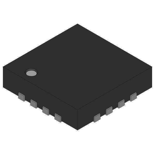
Available in 16 Pin QFN Package
DESCRIPTION/ORDERING INFORMATION
The TPS62110 is a low-noise synchronous step-down dc-dc converter that is ideally suited for systems powered
from a 2-cell Li-ion battery or from a 12-V or 15-V rail.
The TPS62110 is a synchronous PWM converter with integrated N-channel and P-channel power MOSFET
switches. Synchronous rectification is used to increase efficiency and to reduce external component count. To
achieve highest efficiency over a wide load current range, the converter enters a power-saving, pulse-frequency
modulation (PFM) mode at light load currents. Operating frequency is typically 1 MHz, allowing the use of small
inductor and capacitor values. The device can be synchronized to an external clock signal in the range of 0.8
MHz to 1.4 MHz. For low noise operation, the converter can be operated in PWM-only mode. In the shutdown
mode, the current consumption is reduced to less than 2 µA. The TPS62110 is available in the 16-pin (RSA)
QFN package and operates over a free-air temperature range of –40°C to 125°C.
ORDERING INFORMATION (1) (2)
TA
–40°C to 125°C
(1)
(2)
ORDERABLE PART NUMBER
TPS62110QRSARQ1
TOP-SIDE MARKING
TPS62110Q
For the most current package and ordering information, see the Package Option Addendum at the end of this document, or see the TI
web site at www.ti.com.
Package drawings, thermal data, and symbolization are available at www.ti.com/packaging.
1
Please be aware that an important notice concerning availability, standard warranty, and use in critical applications of
Texas Instruments semiconductor products and disclaimers thereto appears at the end of this data sheet.
PRODUCTION DATA information is current as of publication date.
Products conform to specifications per the terms of the Texas
Instruments standard warranty. Production processing does not
necessarily include testing of all parameters.
Copyright © 2010–2012, Texas Instruments Incorporated
�TPS62110-Q1
SLVSA54A – FEBRUARY 2010 – REVISED SEPTEMBER 2012
www.ti.com
This integrated circuit can be damaged by ESD. Texas Instruments recommends that all integrated circuits be handled with
appropriate precautions. Failure to observe proper handling and installation procedures can cause damage.
ESD damage can range from subtle performance degradation to complete device failure. Precision integrated circuits may be more
susceptible to damage because very small parametric changes could cause the device not to meet its published specifications.
ABSOLUTE MAXIMUM RATINGS (1)
over operating free-air temperature range (unless otherwise noted)
PARAMETER
VCC
VALUE
Supply voltage at VIN, VINA
–0.3 V to 20 V
Voltage at SW
VI
–0.3 V to VI
Voltage at EN, SYNC, LBO, PG
–0.3 V to 20 V
Voltage at LBI, FB
–0.3 V to 7 V
IO
Output current at SW
TJ
Maximum junction temperature
Tstg
Storage temperature
ESD
ratings
Human body model (HBM) AEC-Q100 Classification Level H2
(1)
2400 mA
150°C
–65°C to 150°C
2 kV
Charged device model (CDM) AEC-Q100 Classification Level C3B
750 V
Stresses beyond those listed under absolute maximum ratings may cause permanent damage to the device. These are stress ratings
only and functional operation of the device at these or any other conditions beyond those indicated under recommended operating
conditions is not implied. Exposure to absolute-maximum-rated conditions for extended periods may affect device reliability.
DISSIPATION RATINGS (1)
(1)
PACKAGE
TA ≤ 25°C
POWER RATING
DERATING FACTOR
ABOVE TA = 25°C
TA = 70°C
POWER RATING
TA = 85°C
POWER RATING
RSA
2.5 W
25 mW/°C
1.375 W
1W
Based on a thermal resistance of 40 K/W soldered onto a high K board.
RECOMMENDED OPERATING CONDITIONS
VCC
Supply voltage at VIN, VINA
MIN
MAX
3.1
17
V
17
V
125
°C
Maximum voltage at power-good, LBO, EN, SYNC
TJ
2
Operating junction temperature
–40
Submit Documentation Feedback
UNIT
Copyright © 2010–2012, Texas Instruments Incorporated
Product Folder Links: TPS62110-Q1
�TPS62110-Q1
www.ti.com
SLVSA54A – FEBRUARY 2010 – REVISED SEPTEMBER 2012
ELECTRICAL CHARACTERISTICS
VI = 12 V, VO = 3.3 V, IO = 600 mA, EN = VI, TA = –40°C to 125°C (unless otherwise noted)
PARAMETER
TEST CONDITIONS
MIN
TYP
MAX
UNIT
SUPPLY CURRENT
VI
Input voltage range
(1)
I(Q)
Operating quiescent current
I(SD)
Shutdown current
3.1
17
IO = 0 mA, SYNC = GND, VI = 7.2 V,
TA = 25°C (2)
20
IO = 0 mA, SYNC = GND,
VI = 17 V (2)
23
29
EN = GND
1.5
5
EN = GND, TA = 25°C, VI = 7.2 V
1.5
3
V
µA
µA
ENABLE
VIH
EN high-level input voltage
VIL
EN low-level input voltage
1.3
V
0.3
EN trip-point hysteresis
170
IIKG
EN input leakage current
EN = GND or VI, VI = 17 V
I(EN)
EN input current
0.6 V ≤ V(EN) ≤ 4 V
V(UVLO)
Undervoltage lockout threshold
Input voltage falling
Undervoltage lockout hysteresis
0.01
mV
0.2
10
2.8
3
V
µA
µA
3.1
250
V
mV
POWER SWITCH
rDS(ON)
rDS(ON)
VI ≥ 5.4 V, IO = 350 mA
165
VI = 3.5 V, IO = 200 mA
340
VI = 3 V, IO = 100 mA
490
P-channel MOSFET leakage current
VDS = 17 V
0.1
P-channel MOSFET current limit
VI = 7.2 V, VO = 3.3 V
P-channel MOSFET on-resistance
N-channel MOSFET on-resistance
N-channel MOSFET leakage current
250
mΩ
1
2400
VI ≥ 5.4 V, IO = 350 mA
145
VI = 3.5 V, IO = 200 mA
170
VI = 3 V, IO = 100 mA
200
VDS = 17 V
0.1
µA
mA
200
mΩ
3
µA
POWER GOOD OUTPUT, LBI, LBO
V(PG)
Power good trip voltage
Power good delay time
VOL
PG, LBO output low voltage
IOL
PG, LBO sink current
PG, LBO output leakage current
VO – 1.6%
VO ramping positive
50
VO ramping negative
200
V(FB) = 1.1 × VO nominal, IOL = 1 mA
V
µs
0.3
1
V(FB) = VO nominal
Minimum supply voltage for valid
power good, LBI, LBO signal
0.01
mA
0.25
3
Input voltage falling
V
µA
V
VLBI
Low battery input trip voltage
ILBI
LBI input leakage current
10
Low battery input trip-point accuracy
1.5
%
25
mV
VLBI,HYS Low battery input hysteresis
(1)
(2)
1.256
V
100
nA
Not production tested
Device is not switching.
Submit Documentation Feedback
Copyright © 2010–2012, Texas Instruments Incorporated
Product Folder Links: TPS62110-Q1
3
�TPS62110-Q1
SLVSA54A – FEBRUARY 2010 – REVISED SEPTEMBER 2012
www.ti.com
ELECTRICAL CHARACTERISTICS (continued)
VI = 12 V, VO = 3.3 V, IO = 600 mA, EN = VI, TA = –40°C to 125°C (unless otherwise noted)
PARAMETER
TEST CONDITIONS
MIN
TYP
MAX
UNIT
900
1000
1100
kHz
1400
kHz
OSCILLATOR
fS
Oscillator frequency
f(SYNC)
Synchronization range
VIH
SYNC high-level input voltage
VIL
SYNC low-level input voltage
Ilkg
SYNC input leakage current
CMOS-logic clock signal on SYNC pin
800
1.5
SYNC = GND or VIN
V
0.01
SYNC trip-point hysteresis
0.3
V
0.2
µA
170
0.6 V ≤ V(SYNC) ≤ 4 V
SYNC input current
10
Duty cycle of external clock signal
30
mV
20
µA
90
%
16
V
100
nA
OUTPUT
VO
Adjustable output voltage range
VFB
Feedback voltage
1.153
1.153
FB leakage current
10
85°C
Feedback voltage tolerance
(3)
VI = 3.1 V to 17 V,
0 mA < IO < 1500 mA (4)
–2
2
105°C
–2.8
2.8
125°C
–6
6
VI ≥ 3 V (once undervoltage lockout
voltage exceeded)
IO
η
Maximum output current
Efficiency
Duty cycle range for main switches
4
100
VI ≥ 3.5 V
500
VI ≥ 4.3 V
1200
VI ≥ 6 V
1500
VI = 7.2 V, VO = 3.3 V, IO = 600 mA
mA
92
VI = 12 V, VO = 5 V, IO = 600 mA
at 1 MHz
%
10
%
100
%
Minimum ton time for main switch
100
ns
Shutdown temperature
145
°C
1
ms
Start-up time
(3)
(4)
V
IO = 800 mA, VI = 12 V, VO = 3.3 V
Not production tested
The maximum output current depends on the input voltage. See the maximum output current for further restrictions on the minimum
input voltage.
Submit Documentation Feedback
Copyright © 2010–2012, Texas Instruments Incorporated
Product Folder Links: TPS62110-Q1
�TPS62110-Q1
www.ti.com
SLVSA54A – FEBRUARY 2010 – REVISED SEPTEMBER 2012
DEVICE INFORMATION
PGND
SW
SW
PG
RSA PACKAGE
(TOP VIEW)
2
3
4
16 15 14 13
12
Exposed
Thermal
Pad
11
10
5 6 7 8
9
GND
GND
FB
AGND
VINA
1
SYNC
LBO
LBI
PGND
VIN
VIN
EN
TERMINAL FUNCTIONS
TERMINAL
NAME
NO.
I/O
DESCRIPTION
EN
4
I
Enable. A logic high enables the converter; logic low forces the device into shutdown mode reducing the
supply current to less than 2 µA.
FB
10
I
An external resistive divider is connected to this pin to set the output voltage.
LBO
6
O
Open-drain low-battery output. This pin is pulled low if LBI is below its threshold.
GND
11, 12
I
Ground
LBI
7
I
Low-battery input
SW
14, 15
O
Connect the inductor to this pin. This pin is the switch pin and connected to the drain of the internal
power MOSFETS.
PG
13
O
Power good comparator output. This is an open-drain output. A pullup resistor should be connected
between PG and VOUT. The output goes active high when the output voltage is greater than 98.4% of
the nominal value.
PGND
1, 16
I
Power ground. Connect all power grounds to this pin.
AGND
9
I
Analog ground, connect to GND and PGND
Input for synchronization to external clock signal. Synchronizes the converter switching frequency to an
external clock signal with CMOS level:
SYNC
5
I
SYNC = HIGH: Low-noise mode enabled, fixed frequency PWM operation is forced
SYNC = LOW (GND): Power save mode enabled, PFM/PWM mode enabled
VIN
VINA
Thermal pad
2, 3
I
Supply voltage input (power stage)
8
I
Supply voltage input (support circuits)
Connect to AGND
Submit Documentation Feedback
Copyright © 2010–2012, Texas Instruments Incorporated
Product Folder Links: TPS62110-Q1
5
�TPS62110-Q1
SLVSA54A – FEBRUARY 2010 – REVISED SEPTEMBER 2012
www.ti.com
FUNCTIONAL BLOCK DIAGRAM
VI
Current Limit Comparator
+
_
Undervoltage
Lockout
Bias Supply
Vina
REF
Thermal
Shutdown
+
_
Soft Start
V
I
V(COMP)
IAVG Comparator
REF
1-MHz
Oscillator
P-Channel
Power MOSFET
Sawtooth
Generator
Comparator
S
+
_
R
Driver
Shoot-Through
Logic
Control
Logic
SW
N-Channel
Power MOSFET
Comparator High
Comparator Low
Comparator High 2
Load Comparator
+
_
SKIP Comparator
+
_
PG
+
_
Comparator High
+
Gm
_
Comparator Low
+
R2
VREF = 1.153 V
EN
+
_
+
_
(See Note A)
FB
A.
6
LBO
_
R1
Compensation
LBI
1.256 V
PGND
GND
For the adjustable version (TPS62110), the internal feedback divider is disabled and the FB pin is directly connected
to the internal GM amplifier.
Submit Documentation Feedback
Copyright © 2010–2012, Texas Instruments Incorporated
Product Folder Links: TPS62110-Q1
�TPS62110-Q1
www.ti.com
SLVSA54A – FEBRUARY 2010 – REVISED SEPTEMBER 2012
TYPICAL CHARACTERISTICS
Table of Graphs
FIGURE
Efficiency
vs
Output current (1.8 V)
1, 2
Efficiency
vs
Output current (1.5 V)
3, 4
Switching frequency
vs
Input voltage
5
Quiescent current
vs
Input voltage
16
Graphs with VO = 1.8 V were taken using the circuit according to Figure 10.
EFFICIENCY
vs
OUTPUT CURRENT
EFFICIENCY
vs
OUTPUT CURRENT
100
100
90
90
80
4.2 V
80
5V
70
60
Efficiency - %
Efficiency - %
4.2 V
8.4 V
5V
50
12 V
40
30
8.4 V
60
50
40
12 V
30
VO = 1.8 V
o
TA = 25 C
PWM Mode
20
10
0
0.0001
70
0.001
0.01
0.1
1
VO = 1.8 V
o
TA = 25 C
PFM Mode
20
10
10
0
0.0001
IO - Output Current - A
Figure 1.
0.001
0.01
0.1
1
10
IO - Output Current - A
Figure 2.
Submit Documentation Feedback
Copyright © 2010–2012, Texas Instruments Incorporated
Product Folder Links: TPS62110-Q1
7
�TPS62110-Q1
SLVSA54A – FEBRUARY 2010 – REVISED SEPTEMBER 2012
www.ti.com
EFFICIENCY
vs
OUTPUT CURRENT
100
100
90
90
4.2 V
80
70
5V
60
4.2 V
80
Efficiency - %
Efficiency - %
EFFICIENCY
vs
OUTPUT CURRENT
8.4 V
50
40
12 V
30
70
5V
60
8.4 V
50
40
12 V
30
VO = 1.5 V
o
TA = 25 C
PWM Mode
20
10
0
0.0001
0.001
0.01
0.1
10
0
0.0001
10
1
VO = 1.5 V
o
TA = 25 C
PFM Mode
20
0.001
1
Figure 3.
Figure 4.
SWITCHING FREQUENCY
vs
INPUT VOLTAGE
QUIESCENT CURRENT
vs
INPUT VOLTAGE
1000
10
50
VO = 12 V
IO = 100 mA
990
45
o
85 C
40
980
o
970
25 C
960
o
-40 C
950
940
930
Quiescent Current - mA
Switching Frequency - kHz
0.1
IO - Output Current- A
IO - Output Current- A
35
30
20
5
5
6
7 8 9 10 11 12 13 14 15 16 17
VI - Input Voltage - V
o
-40 C
15
910
4
o
25 C
25
10
3
o
85 C
920
900
0
3
4
Figure 5.
8
0.01
5
6
7 8 9 10 11 12 13 14 15 16 17
VI - Input Voltage - V
Figure 6.
Submit Documentation Feedback
Copyright © 2010–2012, Texas Instruments Incorporated
Product Folder Links: TPS62110-Q1
�TPS62110-Q1
www.ti.com
SLVSA54A – FEBRUARY 2010 – REVISED SEPTEMBER 2012
The graphs were generated using the EVM with the setup according to Figure 7 unless otherwise noted. The
output voltage divider was adjusted according to Table 4.
TDK 6.8 µH
SLF7032T-6R8M1R6
Vbat
open
CI 10 µF / 25 V
TDK
C3225X5R1E106K
TPS62110
VIN
VIN
EN
VO
SW
SW
1 MW
1 MW
R1
Cff
PG
VINA
CO 22 µF / 16 V
TDK
C3225X7R1C226M
1 µF
AGND
LBO
FB
LBI
R2
261 kW
SYNC
VIN or
GND
GND GND PwPD PGND PGND
Figure 7. Test Setup
Submit Documentation Feedback
Copyright © 2010–2012, Texas Instruments Incorporated
Product Folder Links: TPS62110-Q1
9
�TPS62110-Q1
SLVSA54A – FEBRUARY 2010 – REVISED SEPTEMBER 2012
www.ti.com
DETAILED DESCRIPTION
OPERATION
The TPS62110 is a synchronous step-down converter that operates with a 1-MHz fixed frequency pulse width
modulation (PWM) at moderate-to-heavy load currents and enters the power save mode at light load current.
During PWM operation, the converter uses a unique fast response voltage mode control scheme with input
voltage feed-forward. Good line and load regulation is achieved with the use of small input and output ceramic
capacitors. At the beginning of each clock cycle initiated by the clock signal (S), the P-channel MOSFET switch
is turned on, and the inductor current ramps up until the comparator trips and the control logic turns the switch
off. The switch is turned off by the current limit comparator if the current limit of the P-channel switch is
exceeded. After the dead time prevents current shoot through, the N-channel MOSFET rectifier is turned on, and
the inductor current ramps down. The next cycle is initiated by the clock signal turning off the N-channel rectifier,
and turning on the P-channel switch.
The error amplifier as well as the input voltage determines the rise time of the sawtooth generator. Therefore,
any change in input voltage or output voltage directly controls the duty cycle of the converter giving a very good
line and load transient regulation.
CONSTANT FREQUENCY MODE OPERATION (SYNC = HIGH)
In constant frequency mode, the output voltage is regulated by varying the duty cycle of the PWM signal in the
range of 100% to 10%. Connecting the SYNC pin to a voltage greater than 1.5 V forces the converter to operate
permanently in the PWM mode even at light or no-load currents. The advantage is that the converter operates
with a fixed switching frequency that allows simple filtering of the switching frequency for noise-sensitive
applications. In this mode, the efficiency is lower compared to the power save mode during light loads. The NMOSFET of the devices stay on even when the current into the output drops to zero. This prevents the device
from going into discontinuous mode, and the device transfers unused energy back to the input. Therefore, there
is no ringing at the output, which usually occurs in discontinuous mode. The duty cycle range in constant
frequency mode is 100% to 10%.
It is possible to switch from forced PWM mode to the power save mode during operation by pulling the SYNC pin
LOW. The flexible configuration of the SYNC pin during operation of the device allows efficient power
management by adjusting the operation of the TPS62110 to the specific system requirements.
POWER SAVE MODE OPERATION (SYNC = LOW)
As the load current decreases, the converter enters the power save mode operation. During power save mode,
the converter operates with reduced switching frequency in pulse frequency modulation (PFM), and with a
minimum quiescent current to maintain high efficiency. Whenever the average output current goes below the skip
threshold, the converter enters the power save mode. The average current depends on the input voltage. It is
about 200 mA at low input voltages and up to 400 mA with maximum input voltage. The average output current
must be below the threshold for at least 32 clock cycles to enter the power save mode. During the power save
mode, the output voltage is monitored with a comparator and the output voltage is regulated in to a typical value
between the nominal output voltage and 0.8% above the nominal output voltage. When the output voltage falls
below the nominal output voltage, the P-channel switch turns on. The P-channel switch is turned off as the peak
switch current is reached. The N-channel rectifier is turned on, and the inductor current ramps down. As the
inductor current approaches zero, the N-channel rectifier is turned off and the switch is turned on starting the
next pulse. When the output voltage can not be reached with a single pulse, the device continues to switch with
its normal operating frequency until the comparator detects the output voltage to be 0.8% above the nominal
output voltage. This control method reduces the quiescent current to 20 µA (typical), and reduces the switching
frequency to a minimum that achieves the highest converter efficiency.
10
Submit Documentation Feedback
Copyright © 2010–2012, Texas Instruments Incorporated
Product Folder Links: TPS62110-Q1
�TPS62110-Q1
www.ti.com
SLVSA54A – FEBRUARY 2010 – REVISED SEPTEMBER 2012
1.6%
0.8%
VO (nominal)
-1.6%
t
Figure 8. Power Save Mode Output Voltage Thresholds
The typical PFM (SKIP) current threshold for the TPS62110 is given by:
VI
I S K IP »
25 W
(1)
Equation 1 is valid for input voltages up to 7 V. For higher voltages, the skip current threshold is not increased
further. The converter enters the fixed frequency PWM mode as soon as the output voltage falls below VO –
1.6% (nominal).
SOFT START
The TPS62110 has an internal soft-start circuit that limits the inrush current during start-up. This prevents
possible voltage drops of the input voltage when a battery or a high-impedance power source is connected to the
input of the TPS62110.
The soft start is implemented as a digital circuit increasing the switch current in steps of 300 mA, 600 mA,
1200 mA. The typical switch current limit is 2.4 A. Therefore, the start-up time depends on the output capacitor
and load current. Typical start-up time with a 22 µF output capacitor and 800-mA load current is 1 ms.
100% DUTY CYCLE LOW DROPOUT OPERATION
The TPS62110 offers the lowest possible input to output voltage difference while still maintaining operation with
the use of the 100% duty cycle mode. In this mode, the P-channel switch is constantly turned on. This is
particularly useful in battery-powered applications to achieve the longest operation time, taking full advantage of
the whole battery voltage range. The minimum input voltage to maintain regulation depends on the load current
and output voltage, and is calculated as:
(
V I min = VO max + I O max × rDS ( on ) max + R( L )
)
(2)
with:
IOmax = maximum output current plus inductor ripple current
rDS(on)max = maximum P-channel switch rDS(on)
R(L) = dc resistance of the inductor
VOmax = nominal output voltage plus maximum output voltage tolerance
Submit Documentation Feedback
Copyright © 2010–2012, Texas Instruments Incorporated
Product Folder Links: TPS62110-Q1
11
�TPS62110-Q1
SLVSA54A – FEBRUARY 2010 – REVISED SEPTEMBER 2012
www.ti.com
ENABLE
Logic low on EN forces the TPS62110 into shutdown. In shutdown, the power switch, drivers, voltage reference,
oscillator, and all other functions are turned off. The supply current is reduced to less than 2 µA in the shutdown
mode. When the device is in thermal shutdown, the bandgap is forced to be switched on even if the device is set
into shutdown by pulling EN to GND.
If an output voltage is present when the device is disabled, which could be due to an external voltage source or a
super capacitor, the reverse leakage current is specified under electrical characteristics. Pulling the enable pin
high starts up the TPS62110 with the soft start. If the EN pin is connected to any voltage other than VI or GND,
an increased leakage current of typically 10 µA and up to 20 µA can occur.
UNDERVOLTAGE LOCKOUT
The undervoltage lockout circuit prevents the device from misoperation at low-input voltages. It prevents the
converter from turning on the switch or rectifier MOSFET under undefined conditions. The minimum input voltage
to start up the TPS62110 is 3.4 V (worst case). The device shuts down at 2.8 V minimum.
SYNCHRONIZATION
If no clock signal is applied, the converter operates with a typical switching frequency of 1 MHz. It is possible to
synchronize the converter to an external clock within a frequency range from 0.8 MHz to 1.4 MHz. The device
automatically detects the rising edge of the first clock and synchronizes immediately to the external clock. If the
clock signal is stopped, the converter automatically switches back to the internal clock and continues operation.
The switch over is initiated if no rising edge on the SYNC pin is detected for a duration of four clock cycles.
Therefore, the maximum delay time can be 6.25 µs if the internal clock has its minimum frequency of 800 kHz.
If the device is synchronized to an external clock, the power save mode is disabled, and the devices stay in
forced PWM mode.
Connecting the SYNC pin to the GND pin enables the power save mode. The converter operates in the PWM
mode at moderate-to-heavy loads, and in the PFM mode during light loads, which maintains high efficiency over
a wide load current range.
POWER GOOD COMPARATOR
The power good (PG) comparator has an open-drain output capable of sinking 1 mA (typical). The PG is active
only when the device is enabled (EN = high). When the device is disabled (EN = low), the PG pin is pulled to
GND.
The PG output is valid only after a 250-µs delay when the device is enabled, and the supply voltage is greater
than the undervoltage lockout V(UVLO). PG is low during the first 250 µs after shutdown and in shutdown.
The PG pin becomes active high when the output voltage exceeds 98.4% (typical) of its nominal value. Leave
the PG pin unconnected when not used.
LOW-BATTERY DETECTOR
The low-battery output (LBO) is an open-drain type which goes low when the voltage at the low-battery input
(LBI) falls below the trip point of 1.256 V ±1.5%. The voltage at which the low-battery warning is issued can be
adjusted with a resistive divider as shown in Figure 9. The sum of resistors (R1 + R2) as well as the sum of (R5
+ R6) is recommended to be in the 100 kΩ to 1 MΩ range for high efficiency at low output current. An external
pullup resistor can be connected to OUT, or any other voltage rail in the voltage range of 0 V to 16 V. During
start-up, the LBO output signal is invalid for the first 500 µs. LBO is high impedance when the device is disabled.
If the low-battery comparator function is not used, connect LBI to ground. The low-battery detector is disabled
when the device is disabled.
The logic level of the LBO pin is not defined for the first 500 µs after EN is pulled high.
When the LBI is used to supervise the battery voltage and shut down the TPS62111 at low-input voltages, the
battery voltage rises when the current drops to zero. The implemented hysteresis on the LBI pin may not be
sufficient for all types of batteries. Figure 9 shows how an additional external hysteresis can be implemented.
12
Submit Documentation Feedback
Copyright © 2010–2012, Texas Instruments Incorporated
Product Folder Links: TPS62110-Q1
�TPS62110-Q1
www.ti.com
SLVSA54A – FEBRUARY 2010 – REVISED SEPTEMBER 2012
6.8 mH
VI = 4.3 V to 17 V
2
3
4
TPS62110
VIN
VIN
EN
SW
SW
15
R3
R5
8
CI = 10 mF
25 V
PG
VINA
1 mF
9
7
AGND
6
FB
10
SYNC
R4
Cff
10 pF
R1
560 k
13
LBO
LBI
5
R6
VO = 3.3 V
14
CO = 22 mF
6.3 V
R2
300 k
R7
GND GND PwPD PGND PGND
11
12
16
1
Figure 9. LBI With Increased Hysteresis
NO LOAD OPERATION
When the converter operates in the forced PWM mode and there is no load connected to the output, the
converter regulates the output voltage by allowing the inductor current to reverse for a short time.
THEORY OF OPERATION AND DESIGN PROCEDURE
Table 1. List of Inductors
MANUFACTURER
(1)
INDUCTANCE
DC RESISTANCE
SATURATION CURRENT
Coilcraft
MSS6132-682
6.8 µH
65 mΩ (max)
1.5 A
Epcos
B82462G4682M
6.8 µH
50 mΩ (max)
1.5 A
Sumida
CDRH5D28-6R2
6.2 µH
33 mΩ (typ)
1.8 A
SLF6028T-6R8M1R5
6.8 µH
35 mΩ (typ)
1.5 A
SLF7032T-6R8M1R6
6.8 µH
41 mΩ (typ)
1.6 A
7447789006
6.8 µH
44 mΩ (typ)
2.75 A
7447779006
6.8 µH
33 mΩ (typ)
3.3 A
744053006
6.2 µH
45 mΩ (typ)
1.8 A
TDK
Wurth
(1)
TYPE
The manufacturer's part numbers are used for test purposes only.
Inductor Selection
The control loop of the TPS62110 requires a certain value for the output inductor and the output capacitor for
stable operation. As long as the nominal value of L × C ≥ 6.2 µH × 22 µF, the control loop has enough phase
margin and the device is stable. Reducing the inductor value without increasing the output capacitor (or vice
versa) may cause stability problems. There are applications where it may be useful to increase the value of the
output capacitor, e.g., for a low transient output voltage change. From a stability point of view, the inductor value
could be decreased to keep the L × C product constant. However, there are drawbacks if the inductor value is
decreased. A low inductor value causes a high inductor ripple current and therefore reduces the maximum dc
output current. Table 2 gives the advantages and disadvantages when designing the inductor and output
capacitor.
Submit Documentation Feedback
Copyright © 2010–2012, Texas Instruments Incorporated
Product Folder Links: TPS62110-Q1
13
�TPS62110-Q1
SLVSA54A – FEBRUARY 2010 – REVISED SEPTEMBER 2012
www.ti.com
Table 2. Advantages and Disadvantages When Designing the Inductor and Output Capacitor
INFLUENCE ON STABILITY
ADVANTAGE
DISADVANTAGE
Less output voltage ripple
Increase Cout (>22 µF)
Uncritical
Decrease Cout (6.8 µH
also
None
Less output voltage overshoot /
undershoot during load transient
Higher output voltage ripple
High output voltage overshoot /
undershoot during load
transient
None
Less gain and phase margin
Increase L (>6.8 µH)
Uncritical
Critical
Decrease L (
22 µF also
High inductor current ripple
especially at high input voltage
and low output voltage
As it is shown in Table 2, the inductor value can be increased to higher values. For good performance, the peakto-peak inductor current ripple should be less than 30% of the maximum dc output current. Especially at input
voltages above 12 V, it makes sense to increase the inductor value to keep the inductor current ripple low. In
such applications, the inductor value can be increased to 10 µH or 22 µH. Values above 22 µH should be
avoided to keep the voltage overshoot during load transient in an acceptable range.
After choosing the inductor value, two additional inductor parameters should be considered:
1. current rating of the inductor
2. dc resistance
The dc resistance of the inductance directly influences the efficiency of the converter. Therefore, an inductor with
lowest dc resistance should be selected for highest efficiency. To avoid saturation of the inductor, the inductor
should be rated at least for the maximum output current plus the inductor ripple current which is calculated as:
1 D I L
=
V O
´
L
V O
V I
´
f
I L m ax =
IO
m ax +
D I L
2
(3)
Where:
f = Switching frequency (1000 kHz typical)
L = Inductor value
ΔIL = Peak-to-peak inductor ripple current
IL(max) = Maximum inductor current
The highest inductor current occurs at maximum VI. A more conservative approach is to select the inductor
current rating just for the maximum switch current of the TPS62110, which is 2.4 A (typically). See Table 1 for
recommended inductors.
OUTPUT CAPACITOR SELECTION
A 22 µF (typical) output capacitor is needed with a 6.8 µH inductor. For an output voltage greater than 5 V, a 33
µF (minimum) output capacitor is required for stability. For best performance, a low ESR ceramic output
capacitor is needed.
The RMS ripple current is calculated as:
VO
VI
L ´ f
1 I R M S (C O ) = V O ´
14
1
´
2 ´
3
Submit Documentation Feedback
(4)
Copyright © 2010–2012, Texas Instruments Incorporated
Product Folder Links: TPS62110-Q1
�TPS62110-Q1
www.ti.com
SLVSA54A – FEBRUARY 2010 – REVISED SEPTEMBER 2012
The overall output ripple voltage is the sum of the voltage spike caused by the output capacitor ESR plus the
voltage ripple caused by charge and discharging the output capacitor:
VO
VI
L ´ f
1 DV O
=
VO ´
æ
1
´ çç
+ RESR
8
C
´
O ´ f
è
ö
÷
÷
ø
(5)
Where the highest output voltage ripple occurs at the highest input voltage VI.
INPUT CAPACITOR SELECTION
The nature of the buck converter is a pulsating input current; therefore, a low ESR input capacitor is required for
best input voltage filtering, and minimizing the interference with other circuits caused by high input voltage
spikes. The input capacitor should have a minimum value of 10 µF and can be increased without any limit for
better input voltage filtering. The input capacitor should be rated for the maximum input ripple current calculated
as:
IR M S
= IO m ax ´
VO
V I
æ
VO
´ çç 1 V I
è
ö
÷÷
ø
(6)
The worst-case RMS ripple current occurs at D = 0.5 and is calculated as: IRMS = IO/2. Ceramic capacitors show
a good performance because of their low ESR value, and they are less sensitive against voltage transients
compared to tantalum capacitors. Place the input capacitor as close as possible to the input pin of the IC for best
performance
FEEDFORWARD CAPACITOR SELECTION
The feedforward capacitor (Cff) is needed to compensate for parasitic capacitance from the feedback pin to GND.
Typically, a value of 4.7 pF to 22 pF is needed for an output voltage divider with a equivalent resistance (R1 in
parallel with R2) in the 150 kΩ range. The value can be chosen based on best transient performance and lowest
output voltage ripple in PFM mode.
RECOMMENDED CAPACITORS
It is recommended that only X5R or X7R ceramic capacitors be used as input/output capacitors. Ceramic
capacitors show a dc-bias effect. This effect reduces the effective capacitance when a dc-bias voltage is applied
across a ceramic capacitor, as on the output and input capacitor of a dc/dc converter. The effect may lead to a
significant capacitance drop especially for high input/output voltages and small capacitor packages. See the
manufacturer's data sheet about the performance with a dc bias voltage applied. It may be necessary to choose
a higher voltage rating or nominal capacitance value to get the required value at the operating point. The
capacitors listed in Table 3 have been tested with the TPS62110 with good performance.
Table 3. List of Capacitors
MANUFACTURER
Taiyo Yuden
PART NUMBER
SIZE
VOLTAGE
CAPACITANCE
TMK316BJ106KL
1206
25 V
10 µF
EMK325BJ226KM
1210
16 V
22 µF
25 V
10 µF
16 V
22 µF
25 V
10 µF
C3225X5R1E106M
TDK
C3225X7R1C226M
C3216X5R1E106MT
1210
1206
TYPE
Ceramic
Ceramic
Submit Documentation Feedback
Copyright © 2010–2012, Texas Instruments Incorporated
Product Folder Links: TPS62110-Q1
15
�TPS62110-Q1
SLVSA54A – FEBRUARY 2010 – REVISED SEPTEMBER 2012
www.ti.com
APPLICATION INFORMATION
6.8 mH
VI = 3.5 V to 17 V
2
TPS62110
VIN
VIN
EN
3
4
SW
SW
15
R3
1 MW
R5
8
CI = 10 mF
25 V
PG
VINA
1 mF
9
AGND
7
5
R6
R4
1 MW
13
LBO
6
FB
10
LBI
VO = 1.8 V
14
R1
220 kW
Cff
10 pF
CO = 2 x 22 mF
6.3 V
R2
390 kW
SYNC
GND GND PwPD PGND PGND
11
A.
12
1
16
For an output voltage lower than 2.5 V, an output capacitor of 33 µF or greater is recommended to improve load
transient.
Figure 10. Standard Connection
V O
= V F B
´
æ VO
R 1 = R 2 ´ çç
è V F B
R 1 + R 2
R 2
ö
÷ - R 2
÷
ø
(7)
VFB = 1.153 V
Table 4. Recommended Resistors
OUTPUT VOLTAGE
R1
R2
NOMINAL VOLTAGE
TYPICAL Cff
9V
680 kΩ
100 kΩ
8.993 V
22 pF
5V
510 kΩ
150 kΩ
5.073 V
10 pF
3.3 V
560 kΩ
300 kΩ
3.305 V
10 pF
2.5 V
390 kΩ
330 kΩ
2.515 V
10 pF
1.8 V
220 kΩ
390 kΩ
1.803 V
10 pF
1.5 V
100 kΩ
330 kΩ
1.502 V
10 pF
6.8 mH
VI = 9.3 V to 17 V
2
3
4
8
CI = 10 mF
25 V
TPS62110
VIN
VIN
EN
SW
SW
7
AGND
13
LBO
6
FB
10
LBI
5
VO = 9 V
14
1 MW
PG
VINA
1 mF
9
15
Cff
R1
680 kW
22 pF
CO = 33 mF
16 V
R2
100 kW
SYNC
GND GND PwPD PGND PGND
11
A.
12
1
16
For an output voltage greater than 5 V, an output capacitor of 33 µF minimum is required for stability.
Figure 11. Application With 9-V Output
16
Submit Documentation Feedback
Copyright © 2010–2012, Texas Instruments Incorporated
Product Folder Links: TPS62110-Q1
�TPS62110-Q1
www.ti.com
SLVSA54A – FEBRUARY 2010 – REVISED SEPTEMBER 2012
REVISION HISTORY
Changes from Original (February, 2010) to Revision A
Page
•
Added AEC-Q100 info to Features ....................................................................................................................................... 1
•
Removed package column in ordering information table ..................................................................................................... 1
•
Added ESD ratings info to Abs Max table ............................................................................................................................ 2
•
Added three rows to feedback voltage tolerance for 85°C, 105°C, and 125°C and updated min and max values ............. 4
Submit Documentation Feedback
Copyright © 2010–2012, Texas Instruments Incorporated
Product Folder Links: TPS62110-Q1
17
�PACKAGE OPTION ADDENDUM
www.ti.com
10-Dec-2020
PACKAGING INFORMATION
Orderable Device
Status
(1)
Package Type Package Pins Package
Drawing
Qty
Eco Plan
(2)
Lead finish/
Ball material
MSL Peak Temp
Op Temp (°C)
Device Marking
(3)
(4/5)
(6)
TPS62110QRSARQ1
ACTIVE
QFN
RSA
16
3000
RoHS & Green
NIPDAU
Level-3-260C-168 HR
-40 to 125
TPS
62110Q
(1)
The marketing status values are defined as follows:
ACTIVE: Product device recommended for new designs.
LIFEBUY: TI has announced that the device will be discontinued, and a lifetime-buy period is in effect.
NRND: Not recommended for new designs. Device is in production to support existing customers, but TI does not recommend using this part in a new design.
PREVIEW: Device has been announced but is not in production. Samples may or may not be available.
OBSOLETE: TI has discontinued the production of the device.
(2)
RoHS: TI defines "RoHS" to mean semiconductor products that are compliant with the current EU RoHS requirements for all 10 RoHS substances, including the requirement that RoHS substance
do not exceed 0.1% by weight in homogeneous materials. Where designed to be soldered at high temperatures, "RoHS" products are suitable for use in specified lead-free processes. TI may
reference these types of products as "Pb-Free".
RoHS Exempt: TI defines "RoHS Exempt" to mean products that contain lead but are compliant with EU RoHS pursuant to a specific EU RoHS exemption.
Green: TI defines "Green" to mean the content of Chlorine (Cl) and Bromine (Br) based flame retardants meet JS709B low halogen requirements of


 工商网监
湘ICP备2023018690号
工商网监
湘ICP备2023018690号