www.ti.com
Table of Contents
User’s Guide
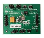
TPS62134x Buck Converter Evaluation Module User's
Guide
ABSTRACT
This user’s guide describes the characteristics, operation, and use of Texas Instrument's TPS62134x evaluation
modules (EVMs). The TPS62134xEVM-595 facilitates the evaluation of the TPS62134x Step-Down Converter
with Low Power Mode Input and Output Voltage Selection device. The device outputs a user-selectable
output voltage between 0.8 V and 1.05 V with a low-power mode from input voltages between 3 V and
17 V. These devices are compatible with the Intel® Skylake platform’s special power requirements for the
VccIO, VccPRIM_CORE, and VccEDRAM / VccEOPIO rails. This user’s guide includes setup instructions for the
hardware, a printed-circuit board layout for the EVM, a schematic diagram, a bill of materials, and test results for
the EVM.
Table of Contents
1 Introduction.............................................................................................................................................................................2
1.1 Performance Specification................................................................................................................................................. 3
1.2 Modifications...................................................................................................................................................................... 3
2 Setup........................................................................................................................................................................................4
2.1 Input/Output Connector Descriptions................................................................................................................................. 4
2.2 Setup..................................................................................................................................................................................4
3 TPS62134xEVM-595 Test Results..........................................................................................................................................5
4 Board Layout...........................................................................................................................................................................6
5 Schematic and Bill of Materials.............................................................................................................................................9
5.1 Schematic.......................................................................................................................................................................... 9
5.2 Bill of Materials.................................................................................................................................................................10
6 Revision History....................................................................................................................................................................11
List of Figures
Figure 1-1. Loop Response Measurement Modification.............................................................................................................. 3
Figure 3-1. Thermal Performance (VIN = 17 V, VOUT = 1.05 V, Load = 3.2 A)............................................................................. 5
Figure 3-2. Loop Measurement (VIN = 12 V, VOUT = 1 V, Load = 3 A)......................................................................................... 5
Figure 4-1. Assembly Layer.........................................................................................................................................................6
Figure 4-2. Top Silk Layer............................................................................................................................................................6
Figure 4-3. Top Layer...................................................................................................................................................................7
Figure 4-4. Internal Layer 1......................................................................................................................................................... 7
Figure 4-5. Internal Layer 2......................................................................................................................................................... 8
Figure 4-6. Bottom Layer............................................................................................................................................................. 8
Figure 5-1. TPS62134xEVM-595 Schematic...............................................................................................................................9
List of Tables
Table 1-1. Performance Specification Summary..........................................................................................................................3
Table 5-1. TPS62134xEVM-595 Bill of Materials.......................................................................................................................10
Trademarks
Intel® is a registered trademark of Intel.
All trademarks are the property of their respective owners.
SLVUA82B – NOVEMBER 2014 – REVISED JUNE 2021
TPS62134x Buck Converter Evaluation Module User's Guide
Submit Document Feedback
Copyright © 2021 Texas Instruments Incorporated
1
�Introduction
www.ti.com
1 Introduction
The TPS62134x is a synchronous, step-down converter in a 3×3-mm, 16-pin QFN package. Four
different versions are available and each has their own EVM: TPS62134AEVM-595 (PWR595-001),
TPS62134BEVM-595 (PWR595-002), TPS62134CEVM-595 (PWR595-003), and TPS62134DEVM-595
(PWR595-004). The versions differ in their output voltage setpoints and low-power mode output voltage. The
TPS62134A is compatible with the Intel Skylake platform's VccIO rail. The TPS62134B and TPS62134D are
compatible with the Intel Skylake platform's VccPRIM_CORE rail. The TPS62134C is compatible with the Intel
Skylake platform's VccEDRAM / VccEOPIO rail.
2
TPS62134x Buck Converter Evaluation Module User's Guide
SLVUA82B – NOVEMBER 2014 – REVISED JUNE 2021
Submit Document Feedback
Copyright © 2021 Texas Instruments Incorporated
�www.ti.com
Introduction
1.1 Performance Specification
Table 1-1 provides a summary of the TPS62134xEVM-595 performance specifications. All specifications are
given for an ambient temperature of 25°C.
Table 1-1. Performance Specification Summary
Specification
Test Conditions
Input voltage
Min
Typ
Max
Unit
3
17
V
Output voltage setpoint
TPS62134AEVM-595, LPM = High
0.85
0.975
V
Output voltage setpoint
TPS62134BEVM-595, LPM = High
0.8
0.95
V
Output voltage setpoint
TPS62134CEVM-595, LPM = High
0.8
1.05
V
Output voltage setpoint
TPS62134DEVM-595, LPM = High
0.85
1
V
0
3.2
A
Output current
Soft-start time
VIN ≥ 5 V
0
Ramp time of VOUT, VOUT = 0.95 V
3
180
A
µs
1.2 Modifications
The printed-circuit board (PCB) for this EVM is designed to accommodate any version of the integrated circuit
(IC). Additional input and output capacitors can also be added. Finally, the loop response of the IC can be
measured.
1.2.1 Input and Output Capacitors
C9 is provided for an additional input capacitor. This capacitor is not required for proper operation but can be
used to reduce the input voltage ripple.
C5, C6, C7, and C8 are provided for additional output capacitors. These capacitors are not required for proper
operation but can be used to reduce the output voltage ripple and to improve the load transient response. The
total output capacitance must remain within the recommended range in the data sheet (SLVSC20) for proper
operation.
1.2.2 Loop Response Measurement
The loop response of the TPS62134xEVM-595 can be measured with two simple changes to the circuitry. First,
install a 10-Ω, 0603-sized resistor across the pads of R2 in the middle of the back of the PCB. Second, cut the
plane between the via near the VOS pin and the output capacitor C2 and the inductor. This change is shown
in Figure 1-1. With these changes, an ac signal (10-mV, peak-to-peak amplitude recommended) can be injected
into the control loop across the added resistor. The results of this test are shown in Figure 3-2.
Figure 1-1. Loop Response Measurement Modification
SLVUA82B – NOVEMBER 2014 – REVISED JUNE 2021
TPS62134x Buck Converter Evaluation Module User's Guide
Submit Document Feedback
Copyright © 2021 Texas Instruments Incorporated
3
�Setup
www.ti.com
2 Setup
This section describes how to properly use the TPS62134xEVM-595.
2.1 Input/Output Connector Descriptions
J1 – VIN
Positive input connection from the input supply for the EVM
J2 – S+/S–
Input voltage sense connections. Measure the input voltage at this point.
J3 – GND
Return connection from the input supply for the EVM
J4 – VOUT
Output voltage connection
J5 – S+/S–
Output voltage sense connections. Measure the output voltage at this point.
J6 – GND
Output return connection
J7 – PG/GND
The PG output appears on pin 1 of this header with a convenient ground on pin 2
J8 – SS/GND
The SS pin voltage appears on pin 2 of this header with a convenient ground on pin 1
J9 – Vdd/GND
An externally applied voltage must be applied on pin 2 of this header with a convenient ground on pin 1. This voltage
must remain between 0.8 V and 6 V. This voltage level sets the logic high level for the VID0, VID1, and LPM pins as
well as the PG pin pull-up voltage.
JP1 – EN
EN pin input jumper. Place the supplied jumper across ON and EN to turn on the IC. Place the jumper across OFF
and EN to turn off the IC.
JP2 – VID0
VID0 pin input jumper. Place the supplied jumper across HIGH and VID0 to set the VID0 pin high. Place the jumper
across LOW and VID0 to set the VID0 pin low.
JP3 – VID1
VID1 pin input jumper. Place the supplied jumper across HIGH and VID1 to set the VID1 pin high. Place the jumper
across LOW and VID1 to set the VID1 pin low.
JP4 – LPM
LPM pin input jumper. Place the supplied jumper across HIGH and LPM to disable the low power mode. Place the
jumper across LOW and LPM to enable the low power mode.
JP5 – PG Pullup
Voltage
PG pin pullup voltage jumper. Place the supplied jumper on JP5 to connect the PG pin pullup resistor to Vdd.
Alternatively, the jumper can be removed and a different voltage can be supplied on pin 1 to pull up the PG pin to a
different level. This externally applied voltage must remain below 7 V.
2.2 Setup
To operate the EVM, set jumpers JP1 through JP5 to the desired positions per Section 2.1. Connect the input
supply to J1 and J3 and connect the load to J4 and J6. Connect a second input supply to J9.
4
TPS62134x Buck Converter Evaluation Module User's Guide
SLVUA82B – NOVEMBER 2014 – REVISED JUNE 2021
Submit Document Feedback
Copyright © 2021 Texas Instruments Incorporated
�www.ti.com
TPS62134xEVM-595 Test Results
3 TPS62134xEVM-595 Test Results
The TPS62134xEVM-595 was used to take the data in the TPS62134x data sheet. See the device data sheet
(SLVSC20) for the performance of this EVM.
60
180
50
150
40
120
30
90
20
60
10
30
0
0
-10
-30
-20
-60
-30
-90
-40
Phase (deg)
Gain (dB)
Figure 3-1. Thermal Performance (VIN = 17 V, VOUT = 1.05 V, Load = 3.2 A)
-120
Gain
-50
-150
Phase
-60
100
1000
10000
100000
-180
1000000
Frequency (Hz)
C001
Figure 3-2. Loop Measurement (VIN = 12 V, VOUT = 1 V, Load = 3 A)
SLVUA82B – NOVEMBER 2014 – REVISED JUNE 2021
TPS62134x Buck Converter Evaluation Module User's Guide
Submit Document Feedback
Copyright © 2021 Texas Instruments Incorporated
5
�Board Layout
www.ti.com
4 Board Layout
This section provides the TPS62134xEVM-595 board layout and illustrations.
Figure 4-1. Assembly Layer
Figure 4-2. Top Silk Layer
6
TPS62134x Buck Converter Evaluation Module User's Guide
SLVUA82B – NOVEMBER 2014 – REVISED JUNE 2021
Submit Document Feedback
Copyright © 2021 Texas Instruments Incorporated
�www.ti.com
Board Layout
Figure 4-3. Top Layer
Figure 4-4. Internal Layer 1
SLVUA82B – NOVEMBER 2014 – REVISED JUNE 2021
TPS62134x Buck Converter Evaluation Module User's Guide
Submit Document Feedback
Copyright © 2021 Texas Instruments Incorporated
7
�Board Layout
www.ti.com
Figure 4-5. Internal Layer 2
Figure 4-6. Bottom Layer
8
TPS62134x Buck Converter Evaluation Module User's Guide
SLVUA82B – NOVEMBER 2014 – REVISED JUNE 2021
Submit Document Feedback
Copyright © 2021 Texas Instruments Incorporated
�www.ti.com
Schematic and Bill of Materials
5 Schematic and Bill of Materials
This section provides the TPS62134xEVM-595 schematic and bill of materials.
5.1 Schematic
Figure 5-1 illustrates the TPS62134xEVM-595 schematic.
VIN
U1
J1
2
1
VIN
3V to 17V
11
12
10
13
J2
2
1
S+
S-
C10
100µF
C9
Open
C1
22uF
9
8
C4
Open
14
J3
PVIN
PVIN
AVIN
EN
VID0
VID1
LPM
2
1
GND
7
SS
FBS
VOS
5
R2
Open
1
TP1
SW
SW
PG
PGND
PGND
AGND
PAD
TPS62134xRGT
2
3
4
15
16
6
1
2
L1
J4
C2
47uF
1µH
XFL4020-102MEB
C5
Open
C6
Open
C7
Open
VOUT
0.7V - 1.05V
3A
C8
Open
1
2
S+
SJ5
Vdd
2
JP5
1
2
GND
J6
1
VIN
1
2
3
ON
EN
OFF
R1
499k
JP1
Vdd
1
2
1
2
3
HIGH
VID0
LOW
PG
GND
J7
JP2
Vdd
1
2
3
HIGH
VID1
LOW
JP3
Vdd
1
2
3
HIGH
/LPM
LOW
JP4
2
1
SS
GND
J8
C3
470pF
Vdd
0.8V to 6V
2
1
Vdd
GND
J9
Figure 5-1. TPS62134xEVM-595 Schematic
SLVUA82B – NOVEMBER 2014 – REVISED JUNE 2021
Submit Document Feedback
TPS62134x Buck Converter Evaluation Module User's Guide
Copyright © 2021 Texas Instruments Incorporated
9
�Schematic and Bill of Materials
www.ti.com
5.2 Bill of Materials
Table 5-1 lists the BOM for this EVM.
Table 5-1. TPS62134xEVM-595 Bill of Materials
Count
PWR595-00
1
PWR595-00
2
PWR595-00
3
PWR595-0
04
Ref Des
Value
Description
Size
Part Number
MFR
1
1
1
1
C1
22uF
Capacitor, Ceramic, 25V, X5R, 20%
0805
GRM21BR61E226ME44
Murata
1
1
1
1
C2
47uF
Capacitor, Ceramic, 6.3V, X5R, 20%
0805
GRM21BR60J476ME15
Murata
1
1
1
1
C3
470pF
Capacitor, Ceramic, 50V, X7R, 10%
0603
GRM188R71H471KA01
D
Murata
1
1
1
1
C10
100uF
Capacitor, Tantalum, 25V, ±10%, 100
mOhm
7361
TPSV107K025R0100
AVX
1
1
1
1
L1
1uH
Inductor, Power, 5.4 A, 10.8 mOhm
4 mm x 4 mm
XFL4020-102MEB
Coilcraft
1
1
1
1
R1
499k
Resistor, Chip, 1/16W, 1%
0603
STD
STD
1
0
0
0
U1
TPS62134A IC, 17-V Input, Step-down Converter with
Low Power Mode Input for Intel Skylake
Platform
3 mm x 3 mm
TPS62134ARGT
TI
0
1
0
0
U1
TPS62134B IC, 17-V Input, Step-down Converter with
Low Power Mode Input for Intel Skylake
Platform
3 mm x 3 mm
TPS62134BRGT
TI
0
0
1
0
U1
TPS62134C IC, 17-V Input, Step-down Converter with
Low Power Mode Input for Intel Skylake
Platform
3 mm x 3 mm
TPS62134CRGT
TI
0
0
0
1
U1
TPS62134D IC, 17-V Input, Step-down Converter with
Low Power Mode Input for Intel Skylake
Platform
3 mm x 3 mm
TPS62134DRGT
TI
The TPS62134xEVM-595 may be populated with TPS62134x (U1) devices that do not contain the correct top
side markings on the top of the device itself. These devices are still fully tested TPS62134x devices and meet
the specified electrical characteristics of the data sheet.
10
TPS62134x Buck Converter Evaluation Module User's Guide
SLVUA82B – NOVEMBER 2014 – REVISED JUNE 2021
Submit Document Feedback
Copyright © 2021 Texas Instruments Incorporated
�www.ti.com
Revision History
6 Revision History
NOTE: Page numbers for previous revisions may differ from page numbers in the current version.
Changes from Revision A (March 2015) to Revision B (June 2021)
Page
• Updated the numbering format for tables, figures, and cross-references throughout the document. ................2
• Updated user's guide title................................................................................................................................... 2
SLVUA82B – NOVEMBER 2014 – REVISED JUNE 2021
TPS62134x Buck Converter Evaluation Module User's Guide
Submit Document Feedback
Copyright © 2021 Texas Instruments Incorporated
11
�Revision History
www.ti.com
Changes from Revision * (November 2014) to Revision A (March 2015)
Page
• Added "TPS62134DEVM-595 (PWR595-004)." to Section 1 ............................................................................ 2
• Added "TPS62134DEVM-595," to Table 1-1 ..................................................................................................... 3
• Added column "PWR595-004" to Table 5-1 .....................................................................................................10
12
TPS62134x Buck Converter Evaluation Module User's Guide
SLVUA82B – NOVEMBER 2014 – REVISED JUNE 2021
Submit Document Feedback
Copyright © 2021 Texas Instruments Incorporated
�IMPORTANT NOTICE AND DISCLAIMER
TI PROVIDES TECHNICAL AND RELIABILITY DATA (INCLUDING DATA SHEETS), DESIGN RESOURCES (INCLUDING REFERENCE
DESIGNS), APPLICATION OR OTHER DESIGN ADVICE, WEB TOOLS, SAFETY INFORMATION, AND OTHER RESOURCES “AS IS”
AND WITH ALL FAULTS, AND DISCLAIMS ALL WARRANTIES, EXPRESS AND IMPLIED, INCLUDING WITHOUT LIMITATION ANY
IMPLIED WARRANTIES OF MERCHANTABILITY, FITNESS FOR A PARTICULAR PURPOSE OR NON-INFRINGEMENT OF THIRD
PARTY INTELLECTUAL PROPERTY RIGHTS.
These resources are intended for skilled developers designing with TI products. You are solely responsible for (1) selecting the appropriate
TI products for your application, (2) designing, validating and testing your application, and (3) ensuring your application meets applicable
standards, and any other safety, security, regulatory or other requirements.
These resources are subject to change without notice. TI grants you permission to use these resources only for development of an
application that uses the TI products described in the resource. Other reproduction and display of these resources is prohibited. No license
is granted to any other TI intellectual property right or to any third party intellectual property right. TI disclaims responsibility for, and you
will fully indemnify TI and its representatives against, any claims, damages, costs, losses, and liabilities arising out of your use of these
resources.
TI’s products are provided subject to TI’s Terms of Sale or other applicable terms available either on ti.com or provided in conjunction with
such TI products. TI’s provision of these resources does not expand or otherwise alter TI’s applicable warranties or warranty disclaimers for
TI products.
TI objects to and rejects any additional or different terms you may have proposed. IMPORTANT NOTICE
Mailing Address: Texas Instruments, Post Office Box 655303, Dallas, Texas 75265
Copyright © 2022, Texas Instruments Incorporated
�