www.ti.com
Table of Contents
User’s Guide
TPS621x0 Buck Converter Evaluation Module User's
Guide
ABSTRACT
This user’s guide describes the characteristics, operation, and use of the Texas Instruments TPS62160 and
TPS62170 evaluation modules (EVM). These EVMs are designed to help the user easily evaluate and test the
operation and functionality of the TPS62160 and TPS62170. This user’s guide includes setup instructions for the
hardware, printed-circuit board layouts for the EVMs, a schematic diagram, a bill of materials, and test results for
the EVMs.
Table of Contents
1 Introduction.............................................................................................................................................................................2
1.1 Background........................................................................................................................................................................ 2
1.2 Performance Specification................................................................................................................................................. 2
1.3 Modifications...................................................................................................................................................................... 2
2 Setup........................................................................................................................................................................................4
2.1 Input/Output Connector Descriptions................................................................................................................................. 4
2.2 Setup..................................................................................................................................................................................4
3 TPS621x0EVM-627 Test Results............................................................................................................................................5
4 Board Layout......................................................................................................................................................................... 11
5 Schematic and Bill of Materials...........................................................................................................................................13
5.1 Schematic........................................................................................................................................................................ 13
5.2 Bill of Materials.................................................................................................................................................................14
6 Revision History................................................................................................................................................................... 14
List of Figures
Figure 1-1. Loop Response Measurement Modification.............................................................................................................. 3
Figure 3-1. Efficiency................................................................................................................................................................... 5
Figure 3-2. Load Regulation........................................................................................................................................................ 5
Figure 3-3. Line Regulation With Iout = 0.5 A..............................................................................................................................5
Figure 3-4. Loop Response With Vin = 12 V and Iout = 0.5 A..................................................................................................... 6
Figure 3-5. Input Voltage Ripple With Vin = 12 V and Iout = 1 A................................................................................................. 6
Figure 3-6. Output Voltage Ripple With Vin = 12 V and Iout = 1 A.............................................................................................. 7
Figure 3-7. Load Transient Response With Vin = 12 V................................................................................................................7
Figure 3-8. Start-Up on Vin With 0.5-A Load............................................................................................................................... 8
Figure 3-9. Start-Up on EN with 0.5-A Load................................................................................................................................ 8
Figure 3-10. Shutdown on EN With 0.5-A Load...........................................................................................................................9
Figure 3-11. Prebias Start-Up and Shutdown on EN With 0.5-A Load........................................................................................ 9
Figure 3-12. Thermal Performance With Vin = 12 V and Iout = 1 A.......................................................................................... 10
Figure 4-1. Assembly Layer....................................................................................................................................................... 11
Figure 4-2. Top Layer Routing....................................................................................................................................................11
Figure 4-3. Bottom Layer Routing..............................................................................................................................................12
Figure 5-1. TPS621x0EVM-627 Schematic...............................................................................................................................13
List of Tables
Table 1-1. Performance Specification Summary..........................................................................................................................2
Table 5-1. TPS621x0EVM-627 Bill of Materials.........................................................................................................................14
SLVU483A – OCTOBER 2011 – REVISED JUNE 2021
Submit Document Feedback
TPS621x0 Buck Converter Evaluation Module User's Guide
Copyright © 2021 Texas Instruments Incorporated
1
�Introduction
www.ti.com
1 Introduction
The TPS62160 is a 1-A, synchronous, step-down converter in a 2x2-mm, 8-pin WSON package. Both fixed and
adjustable output voltage units are available.
The TPS62170 is a 0.5-A, synchronous, step-down converter in a 2x2-mm, 8-pin WSON package. Both fixed
and adjustable output voltage units are available.
1.1 Background
The TPS62160EVM-627 (HPA627-001) uses the TPS62160 adjustable version and is set to a 3.3-V output. The
EVM operates with full-rated performance with an input voltage between 3.7 V and 17 V.
The TPS62170EVM-627 (HPA627-002) uses the TPS62170 adjustable version and is set to a 3.3-V output. The
EVM operates with full-rated performance with an input voltage between 3.7 V and 17 V.
1.2 Performance Specification
Table 1-1 provides a summary of the TPS621x0EVM-627 performance specifications. All specifications are given
for an ambient temperature of 25°C.
Table 1-1. Performance Specification Summary
Specification
Test Conditions
Input Voltage
Min
Typ
Max
17
V
3.327
3.427
V
3.7
3.227
Unit
Output Voltage
PWM Mode of Operation
Output Current
TPS62160EVM-627
0
1000
mA
TPS62170EVM-627
0
500
mA
Peak Efficiency
93.1%
Soft-Start Time
180
µs
1.3 Modifications
The printed-circuit board (PCB) for this EVM is designed to accommodate both the fixed and adjustable voltage
versions of this integrated circuit (IC). Additional input and output capacitors can also be added. Finally, the loop
response of the IC can be measured.
1.3.1 Fixed Output Operation
U1 can be replaced with the fixed-voltage version of the IC for evaluation. For fixed-voltage version operation,
replace R2 with a 0-Ω resistor and remove R1.
1.3.2 Input and Output Capacitors
C4 is provided for an additional input capacitor. This capacitor is not required for proper operation but can be
used to reduce the input voltage ripple.
C3 is provided for an additional output capacitor. This capacitor is not required for proper operation but can
be used to reduce the output voltage ripple and to improve the load transient response. The total output
capacitance must remain within the recommended range in the data sheet for proper operation.
1.3.3 Loop Response Measurement
The loop response of the TPS621x0EVM-627 can be measured with two simple changes to the circuitry. First,
install a 10-Ω resistor across the pads in the middle of the back of the PCB. The pads are spaced to allow
installation of 0805- or 0603-sized resistors. Second, cut the short section of trace between the via on the output
voltage and the trace that connects to the VOS pin via. These changes are shown in Figure 1-1. With these
changes, an ac signal (10-mV, peak-to-peak amplitude recommended) can be injected into the control loop
across the added resistor.
2
TPS621x0 Buck Converter Evaluation Module User's Guide
Copyright © 2021 Texas Instruments Incorporated
SLVU483A – OCTOBER 2011 – REVISED JUNE 2021
Submit Document Feedback
�www.ti.com
Introduction
Added Resistor
Cut This Trace
Figure 1-1. Loop Response Measurement Modification
SLVU483A – OCTOBER 2011 – REVISED JUNE 2021
Submit Document Feedback
TPS621x0 Buck Converter Evaluation Module User's Guide
Copyright © 2021 Texas Instruments Incorporated
3
�Setup
www.ti.com
2 Setup
This section describes how to properly use the TPS621x0EVM-627.
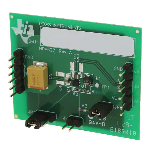
2.1 Input/Output Connector Descriptions
J1 – VIN
Positive input connection from the input supply for the EVM.
J2 – S+/S-
Input voltage sense connections. Measure the input voltage at this point.
J3 – GND
Return connection from the input supply for the EVM.
J4 – VOUT
Output voltage connection.
J5 – S+/S-
Output voltage sense connections. Measure the output voltage at this point.
J6 – GND
Output return connection.
J7 – PG/GND
The PG output appears on pin 1 of this header with a convenient ground on pin 2.
JP1 – EN
EN pin input jumper. Place the supplied jumper across ON and EN to turn on the IC. Place the jumper across OFF
and EN to turn off the IC.
JP2 – PG Pullup
Voltage
PG pin pullup voltage jumper. Place the supplied jumper on JP2 to connect the PG pin pullup resistor to Vout.
Alternatively, the jumper can be removed and a different voltage can be supplied on pin 1 to pull up the PG pin to a
different level. This externally applied voltage must remain below 7 V.
2.2 Setup
To operate the EVM, set jumpers JP1 through JP2 to the desired positions per Section 2.1. Connect the input
supply to J1 and J3 and connect the load to J4 and J6.
4
TPS621x0 Buck Converter Evaluation Module User's Guide
Copyright © 2021 Texas Instruments Incorporated
SLVU483A – OCTOBER 2011 – REVISED JUNE 2021
Submit Document Feedback
�www.ti.com
TPS621x0EVM-627 Test Results
3 TPS621x0EVM-627 Test Results
This section provides test results of the TPS621x0EVM-627.
100
95
VIN = 5 V
90
VIN = 9 V
85
Efficiency (%)
80
75
VIN = 12 V
70
VIN = 15 V
VIN = 17 V
65
60
55
50
45
40
0.1
1
10
100
1000
Current (mA)
Figure 3-1. Efficiency
0.5
VIN = 15 V
0.4
VIN = 17 V
Load Regulation (%)
0.3
VIN = 12 V
0.2
0.1
VIN = 9 V
0
VIN = 5 V
-0.1
-0.2
0.1
1
10
Current (mA)
100
1000
Figure 3-2. Load Regulation
0.15
Line Regulation (%)
0.1
0.05
0
-0.05
-0.1
3
5
7
9
11
VI - Input Voltage - (V)
13
15
17
Figure 3-3. Line Regulation With Iout = 0.5 A
SLVU483A – OCTOBER 2011 – REVISED JUNE 2021
Submit Document Feedback
TPS621x0 Buck Converter Evaluation Module User's Guide
Copyright © 2021 Texas Instruments Incorporated
5
�TPS621x0EVM-627 Test Results
www.ti.com
60
180
Gain - dB
150
40
120
30
90
20
60
10
30
Gain
0
0
-10
-30
-20
-60
-30
-90
-40
-120
-50
Phase - deg.
Phase
50
-150
-60
1k
10k
100k
-180
1M
f - Frequency - Hz
Figure 3-4. Loop Response With Vin = 12 V and Iout = 0.5 A
Vin (AC Coupled) 20 mV/div
Iind 500 mA/div
SW 10 V/div
t - Time - 200 ns/div
Figure 3-5. Input Voltage Ripple With Vin = 12 V and Iout = 1 A
6
TPS621x0 Buck Converter Evaluation Module User's Guide
Copyright © 2021 Texas Instruments Incorporated
SLVU483A – OCTOBER 2011 – REVISED JUNE 2021
Submit Document Feedback
�www.ti.com
TPS621x0EVM-627 Test Results
Vout (AC Coupled) 10 mV/div
Iind 500 mA/div
SW 10 V/div
t - Time - 500 ns/div
Figure 3-6. Output Voltage Ripple With Vin = 12 V and Iout = 1 A
Vout (AC Coupled) 20 mV/div
Iout 500 mA/div
500 mA to 750 mA Load step
t - Time - 2 ms/div
Figure 3-7. Load Transient Response With Vin = 12 V
SLVU483A – OCTOBER 2011 – REVISED JUNE 2021
Submit Document Feedback
TPS621x0 Buck Converter Evaluation Module User's Guide
Copyright © 2021 Texas Instruments Incorporated
7
�TPS621x0EVM-627 Test Results
www.ti.com
Vin 5 V/div
EN 5 V/div
PG 2 V/div
Vout 1 V/div
t - Time - 50 ms/div
Figure 3-8. Start-Up on Vin With 0.5-A Load
Vin 10 V/div
EN 10 V/div
PG 2 V/div
Vout 1 V/div
t - Time - 50 ms/div
Figure 3-9. Start-Up on EN with 0.5-A Load
8
TPS621x0 Buck Converter Evaluation Module User's Guide
Copyright © 2021 Texas Instruments Incorporated
SLVU483A – OCTOBER 2011 – REVISED JUNE 2021
Submit Document Feedback
�www.ti.com
TPS621x0EVM-627 Test Results
Vin 10 V/div
EN 10 V/div
PG 2 V/div
Vout 1 V/div
t - Time - 200 ms/div
Figure 3-10. Shutdown on EN With 0.5-A Load
Vin 10 V/div
EN 2 V/div
PG 2 V/div
Vout 1 V/div
1.5 V Pre-bias
t - Time - 100 ms/div
Figure 3-11. Prebias Start-Up and Shutdown on EN With 0.5-A Load
SLVU483A – OCTOBER 2011 – REVISED JUNE 2021
Submit Document Feedback
TPS621x0 Buck Converter Evaluation Module User's Guide
Copyright © 2021 Texas Instruments Incorporated
9
�TPS621x0EVM-627 Test Results
www.ti.com
Figure 3-12. Thermal Performance With Vin = 12 V and Iout = 1 A
10
TPS621x0 Buck Converter Evaluation Module User's Guide
Copyright © 2021 Texas Instruments Incorporated
SLVU483A – OCTOBER 2011 – REVISED JUNE 2021
Submit Document Feedback
�www.ti.com
Board Layout
4 Board Layout
This section provides the TPS621x0EVM-627 board layout and illustrations.
Figure 4-1. Assembly Layer
Figure 4-2. Top Layer Routing
SLVU483A – OCTOBER 2011 – REVISED JUNE 2021
Submit Document Feedback
TPS621x0 Buck Converter Evaluation Module User's Guide
Copyright © 2021 Texas Instruments Incorporated
11
�Board Layout
www.ti.com
Figure 4-3. Bottom Layer Routing
12
TPS621x0 Buck Converter Evaluation Module User's Guide
Copyright © 2021 Texas Instruments Incorporated
SLVU483A – OCTOBER 2011 – REVISED JUNE 2021
Submit Document Feedback
�www.ti.com
Schematic and Bill of Materials
5 Schematic and Bill of Materials
This section provides the TPS621x0EVM-627 schematic and bill of materials.
+
5.1 Schematic
Figure 5-1. TPS621x0EVM-627 Schematic
SLVU483A – OCTOBER 2011 – REVISED JUNE 2021
Submit Document Feedback
TPS621x0 Buck Converter Evaluation Module User's Guide
Copyright © 2021 Texas Instruments Incorporated
13
�Schematic and Bill of Materials
www.ti.com
5.2 Bill of Materials
Table 5-1. TPS621x0EVM-627 Bill of Materials
Count
-001
-002
RefDes
Value
Description
Size
Part Number
MFR
1
1
C1
10 µF
Capacitor, Ceramic, 25V, X5R, 20%
0805
Std
Std
1
1
C2
22 µF
Capacitor, Ceramic, 6.3V, X5R, 20%
0805
Std
Std
1
1
C5
68 µF
Capacitor, Tantalum, 35V, 68uF, ±20%
7361[V]
TPSV686M035R0150
AVX
1
1
L1
2.2 µH
Inductor, SMT, 2.2 uH, 1.4A, 60-milliohm
2.80 X 3.00 mm
VLF3012ST-2R2M1R4
TDK
1
1
R1
1.21M
Resistor, Chip, 1/16W, 1%
0603
Std
Std
1
1
R2
383k
Resistor, Chip, 1/16W, 1%
0603
Std
Std
1
1
R3
100k
Resistor, Chip, 1/16W, 1%
0603
Std
Std
1
0
U1
TPS62160DSG
IC, 17V 1A Buck Converter
2 x 2 mm WSON
TPS62160DSG
TI
0
1
U1
TPS62170DSG
IC, 17V 0.5A Buck Converter
2 x 2 mm WSON
TPS62170DSG
TI
6 Revision History
NOTE: Page numbers for previous revisions may differ from page numbers in the current version.
Changes from Revision * (October 2011) to Revision A (June 2021)
Page
• Updated user's guide title................................................................................................................................... 2
• Updated the numbering format for tables, figures, and cross-references throughout the document. ................2
14
TPS621x0 Buck Converter Evaluation Module User's Guide
Copyright © 2021 Texas Instruments Incorporated
SLVU483A – OCTOBER 2011 – REVISED JUNE 2021
Submit Document Feedback
�IMPORTANT NOTICE AND DISCLAIMER
TI PROVIDES TECHNICAL AND RELIABILITY DATA (INCLUDING DATA SHEETS), DESIGN RESOURCES (INCLUDING REFERENCE
DESIGNS), APPLICATION OR OTHER DESIGN ADVICE, WEB TOOLS, SAFETY INFORMATION, AND OTHER RESOURCES “AS IS”
AND WITH ALL FAULTS, AND DISCLAIMS ALL WARRANTIES, EXPRESS AND IMPLIED, INCLUDING WITHOUT LIMITATION ANY
IMPLIED WARRANTIES OF MERCHANTABILITY, FITNESS FOR A PARTICULAR PURPOSE OR NON-INFRINGEMENT OF THIRD
PARTY INTELLECTUAL PROPERTY RIGHTS.
These resources are intended for skilled developers designing with TI products. You are solely responsible for (1) selecting the appropriate
TI products for your application, (2) designing, validating and testing your application, and (3) ensuring your application meets applicable
standards, and any other safety, security, regulatory or other requirements.
These resources are subject to change without notice. TI grants you permission to use these resources only for development of an
application that uses the TI products described in the resource. Other reproduction and display of these resources is prohibited. No license
is granted to any other TI intellectual property right or to any third party intellectual property right. TI disclaims responsibility for, and you
will fully indemnify TI and its representatives against, any claims, damages, costs, losses, and liabilities arising out of your use of these
resources.
TI’s products are provided subject to TI’s Terms of Sale or other applicable terms available either on ti.com or provided in conjunction with
such TI products. TI’s provision of these resources does not expand or otherwise alter TI’s applicable warranties or warranty disclaimers for
TI products.
TI objects to and rejects any additional or different terms you may have proposed. IMPORTANT NOTICE
Mailing Address: Texas Instruments, Post Office Box 655303, Dallas, Texas 75265
Copyright © 2022, Texas Instruments Incorporated
�