Sample &
Buy
Product
Folder
Technical
Documents
Support &
Community
Tools &
Software
Reference
Design
TPS62230, TPS62231, TPS62232, TPS62233, TPS62234, TPS62235, TPS62236
TPS62237, TPS62238, TPS62239, TPS622310, TPS622311, TPS622312
TPS622313, TPS622314, TPS622315, TPS622316, TPS622317, TPS622318, TPS622319
SLVS941G – APRIL 2009 – REVISED AUGUST 2016
TPS6223xx 2-MHz and 3-MHz Ultra Small Step-Down Converter in 1 x 1.5 USON Package
1 Features
•
•
•
•
1
•
•
•
•
•
•
•
•
•
•
2 MHz / 3 MHz Switching Frequency
Up to 94% Efficiency
Output Peak Current up to 500 mA
Operating Junction Temperature of –40°C to
125°C
High PSRR (up to 90 dB)
Small External Output Filter Components 1 μH
and 4.7 μF
VIN range from 2.05 V to 6 V
Optimized Power-Save Mode for Low Output
Ripple Voltage
Forced PWM Mode Operation
Typ. 22-μA Quiescent Current
100% Duty Cycle for Lowest Dropout
Small 1-mm × 1.5-mm × 0.6-mm USON Package
12-mm2 Minimum Solution Size
Supports 0.6-mm Maximum Solution Height
2 Applications
•
•
•
•
•
With a wide input voltage range of 2.05 V to 6 V, the
device supports applications powered by Li-Ion
batteries with extended voltage range. The minimum
input voltage of 2.05 V allows as well the operation
from Li-primary or two alkaline batteries. Different
fixed output voltage versions are available from 1.0 V
to 3.3 V.
The TPS6223x series features switch frequency up to
3.8 MHz. At medium to heavy loads, the converter
operates in pulse width modulation (PWM) mode and
automatically enters power-save mode operation at
light load currents to maintain high efficiency over the
entire load current range.
Because of its excellent power supply rejection ratio
(PSRR) and AC load regulation performance, the
device is also suitable to replace linear regulators to
obtain better power conversion efficiency.
The power-save mode in TPS6223x reduces the
quiescent current consumption down to 22 μA during
light load operation. It is optimized to achieve very
low output voltage ripple even with small external
component and features excellent AC load regulation.
For very noise-sensitive applications, the device can
be forced to PWM mode operation over the entire
load range by pulling the MODE pin high. In the
shutdown mode, the current consumption is reduced
to less than 1 μA. The TPS6223x operates over a
junction temperature range of –40°C to 125°C. It is
available in a 1 mm × 1.5 mm × 0.6 mm 6-pin SON
package.
LDO Replacement
Portable Audio, Portable Media
Low Power Wireless
Low Power DSP Core Supply
Digital Cameras
3 Description
The TPS6223x device family is a high-frequency,
synchronous, step-down DC – DC converter
optimized for battery powered portable applications. It
supports up to 500-mA output current and allows the
use of tiny and low-cost chip inductors and
capacitors.
Device Information(1)
PART NUMBER
TPS6223xx
CIN
2.2 mF
L
1/2.2 mH
TPS62231
VIN
EN
MODE
SW
FB
GND
BODY SIZE (NOM)
USON (6)
1.45 mm x 1.00 mm
(1) For all available packages, see the orderable addendum at
the end of the data sheet.
Typical Application Schematic
VIN
2.05 V to 6 V
PACKAGE
Small PCB Layout Size
L1
VOUT
1.8 V
COUT
4.7 mF
C1
Copyright © 2016, Texas Instruments Incorporated
V IN
Total area
is less than
12mm²
C2
GND
V OUT
1
An IMPORTANT NOTICE at the end of this data sheet addresses availability, warranty, changes, use in safety-critical applications,
intellectual property matters and other important disclaimers. PRODUCTION DATA.
�TPS62230, TPS62231, TPS62232, TPS62233, TPS62234, TPS62235, TPS62236
TPS62237, TPS62238, TPS62239, TPS622310, TPS622311, TPS622312
TPS622313, TPS622314, TPS622315, TPS622316, TPS622317, TPS622318, TPS622319
SLVS941G – APRIL 2009 – REVISED AUGUST 2016
www.ti.com
Table of Contents
1
2
3
4
5
6
7
8
Features ..................................................................
Applications ...........................................................
Description .............................................................
Revision History.....................................................
Device Comparison Table.....................................
Pin Configuration and Functions .........................
Specifications.........................................................
1
1
1
2
4
5
5
7.1
7.2
7.3
7.4
7.5
7.6
5
5
6
6
7
8
Absolute Maximum Ratings ......................................
ESD Ratings..............................................................
Recommended Operating Conditions.......................
Thermal Information ..................................................
Electrical Characteristics...........................................
Typical Characteristics ..............................................
Detailed Description .............................................. 9
8.1
8.2
8.3
8.4
Overview ................................................................... 9
Functional Block Diagram ....................................... 10
Feature Description................................................. 10
Device Functional Modes........................................ 11
9
Application and Implementation ........................ 13
9.1 Application Information............................................ 13
9.2 Typical Application .................................................. 13
9.3 System Examples ................................................... 26
10 Power Supply Recommendations ..................... 27
11 Layout................................................................... 27
11.1 Layout Guidelines ................................................. 27
11.2 Layout Example .................................................... 27
12 Device and Documentation Support ................. 28
12.1
12.2
12.3
12.4
12.5
12.6
12.7
Device Support......................................................
Related Links ........................................................
Receiving Notification of Documentation Updates
Community Resources..........................................
Trademarks ...........................................................
Electrostatic Discharge Caution ............................
Glossary ................................................................
28
28
28
29
29
29
29
13 Mechanical, Packaging, and Orderable
Information ........................................................... 29
4 Revision History
NOTE: Page numbers for previous revisions may differ from page numbers in the current version.
Changes from Revision F (July 2015) to Revision G
Page
•
Added device TPS622319 ..................................................................................................................................................... 4
•
Deleted Package information from Device Comparison Table, and added footnote ............................................................ 4
•
Added Receiving Notification of Documentation Updates section ....................................................................................... 28
Changes from Revision E (December 2010) to Revision F
•
Page
Added Pin Configuration and Functions section, ESD Ratings table, Feature Description section, Device Functional
Modes, Application and Implementation section, Power Supply Recommendations section, Layout section, Device
and Documentation Support section, and Mechanical, Packaging, and Orderable Information section .............................. 1
Changes from Revision D (August 2010) to Revision E
•
Page
Added device number TPS622318......................................................................................................................................... 1
Changes from Revision C (April 2010) to Revision D
Page
•
Added device numbers TPS622315, TPS622316, and TPS622317...................................................................................... 1
•
Changed data sheet status from "Product Mix" to "Production Data" .................................................................................... 1
•
Deleted table footnote regarding "other voltage options" ....................................................................................................... 4
Changes from Revision B (December 2009) to Revision C
•
2
Page
Added device numbers TPS622312, TPS622313, and TPS622314...................................................................................... 1
Submit Documentation Feedback
Copyright © 2009–2016, Texas Instruments Incorporated
Product Folder Links: TPS62230 TPS62231 TPS62232 TPS62233 TPS62234 TPS62235 TPS62236 TPS62237
TPS62238 TPS62239 TPS622310 TPS622311 TPS622312 TPS622313 TPS622314 TPS622315 TPS622316
TPS622317 TPS622318 TPS622319
�TPS62230, TPS62231, TPS62232, TPS62233, TPS62234, TPS62235, TPS62236
TPS62237, TPS62238, TPS62239, TPS622310, TPS622311, TPS622312
TPS622313, TPS622314, TPS622315, TPS622316, TPS622317, TPS622318, TPS622319
www.ti.com
SLVS941G – APRIL 2009 – REVISED AUGUST 2016
Changes from Revision A (August 2009) to Revision B
Page
•
Added device numbers TPS62235, TPS62236, TPS62237, TPS622311.............................................................................. 1
•
Changed the Title From: 3 MHz Ultra Small Step Down Converter in 1x1.5 SON Package To: 2 MHz / 3 MHz Ultra
Small Step Down Converter in 1x1.5 SON Package.............................................................................................................. 1
•
Changed Feature: From: 3 MHz switch frequency To: 2 MHz / 3 MHz switch frequency ..................................................... 1
•
Added Figure 6, Figure 7, and Figure 10 ............................................................................................................................. 16
•
Added Figure 15 ................................................................................................................................................................... 17
•
Added Figure 24, and Figure 25........................................................................................................................................... 19
•
Added Figure 32 ................................................................................................................................................................... 21
•
Added Figure 41, and Figure 42........................................................................................................................................... 23
Changes from Original (April 2009) to Revision A
•
Page
Added device numbers TPS62233, TPS62234, TPS62238, TPS62239, and TPS622310 to the data sheet ....................... 1
Copyright © 2009–2016, Texas Instruments Incorporated
Submit Documentation Feedback
Product Folder Links: TPS62230 TPS62231 TPS62232 TPS62233 TPS62234 TPS62235 TPS62236 TPS62237
TPS62238 TPS62239 TPS622310 TPS622311 TPS622312 TPS622313 TPS622314 TPS622315 TPS622316
TPS622317 TPS622318 TPS622319
3
�TPS62230, TPS62231, TPS62232, TPS62233, TPS62234, TPS62235, TPS62236
TPS62237, TPS62238, TPS62239, TPS622310, TPS622311, TPS622312
TPS622313, TPS622314, TPS622315, TPS622316, TPS622317, TPS622318, TPS622319
SLVS941G – APRIL 2009 – REVISED AUGUST 2016
www.ti.com
5 Device Comparison Table
OUTPUT VOLTAGE
FREQUENCY
[MHz]
Pulldown
EN, MODE
PACKAGE
MARKING
TPS62230
2.5 V
3
no
GV
TPS62231
1.8 V
3
no
GW
TPS62232
1.2 V
3
no
GX
TPS62239
1.0 V
3
no
OP
TPS622311
1.1V
2
no
PA
TPS622315
1.15V
2
no
RI
TPS62235
1.2V
2
no
OQ
TPS622318
1.25V
3
no
ST
TPS622319
1.2V
2
yes
3O
TPS622313
1.3 V
3
no
QF
TPS622314
1.5 V
3
no
QG
TPS62236
1.85V
2
no
OR
TPS622312
2.0 V
3
no
QE
TPS62234
2.1 V
3
no
OH
TPS62238
2.25 V
3
no
ON
TPS622310
2.3 V
3
no
OT
TPS622316
2.7 V
3
no
RJ
TPS622317
2.9 V
3
no
RK
TPS62233
3.0 V
3
no
OG
TPS62237
3.3 V
2
no
OS
PART NUMBER (1)
(1)
4
For detailed ordering information see the PACKAGE OPTION ADDENDUM at the end of this data sheet.
Submit Documentation Feedback
Copyright © 2009–2016, Texas Instruments Incorporated
Product Folder Links: TPS62230 TPS62231 TPS62232 TPS62233 TPS62234 TPS62235 TPS62236 TPS62237
TPS62238 TPS62239 TPS622310 TPS622311 TPS622312 TPS622313 TPS622314 TPS622315 TPS622316
TPS622317 TPS622318 TPS622319
�TPS62230, TPS62231, TPS62232, TPS62233, TPS62234, TPS62235, TPS62236
TPS62237, TPS62238, TPS62239, TPS622310, TPS622311, TPS622312
TPS622313, TPS622314, TPS622315, TPS622316, TPS622317, TPS622318, TPS622319
www.ti.com
SLVS941G – APRIL 2009 – REVISED AUGUST 2016
6 Pin Configuration and Functions
DRY Package
6-Pin USON
Top View
MODE 1
6
FB
SW 2
5 EN
VIN 3
4
GND
Pin Functions
PIN
NAME
NO
TYPE
DESCRIPTION
VIN
3
Power
VIN power supply pin
GND
4
Power
GND supply pin
EN
5
Input
This is the enable pin of the device. Pulling this pin to low forces the device into shutdown mode.
Pulling this pin to high enables the device. This pin must be terminated except for the
TPS622319, which has an integrated 1MΩ always active pull-down resistor.
SW
2
Output
This is the switch pin and is connected to the internal MOSFET switches. Connect the inductor to
this terminal
FB
6
Input
Feedback pin for the internal regulation loop. Connect this pin directly to the output capacitor.
MODE
1
Input
MODE pin = High forces the device to operate in PWM mode. Mode = Low enables the power
save mode with automatic transition from pulse frequency modulation (PFM) to pulse width
modulation (PWM) mode. This pin must be terminated except for the TPS622319 , which has an
integrated 1MΩ always active pull-down resistor.
7 Specifications
7.1 Absolute Maximum Ratings
over operating free-air temperature range (unless otherwise noted) (1)
MIN
Voltage at VIN and SW pin
VIN
TJ
(2)
(2)
UNIT
–0.3
7
V
Voltage at EN, MODE pin (2)
–0.3
VIN +0.3, ≤7
V
Voltage at FB pin (2)
–0.3
3.6
V
Peak output current
Internally limited
Power dissipation
Internally limited
Operating junction Temperature Range
Tstg Storage Temperature Range
(1)
MAX
A
–40
150
°C
–65
150
°C
Stresses beyond those listed under Absolute Maximum Ratings may cause permanent damage to the device. These are stress ratings
only and functional operation of the device at these or any other conditions beyond those indicated under Recommended Operating
Conditions is not implied. Exposure to absolute–maximum–rated conditions for extended periods may affect device reliability.
All voltage values are with respect to network ground terminal.
7.2 ESD Ratings
VALUE
V(ESD)
(1)
(2)
Electrostatic discharge
Human body model (HBM), per ANSI/ESDA/JEDEC JS-001, all
pins (1)
±2000
Charge- device model (CDM), per JEDEC specification JESD22C101, all pins (2)
±1000
UNIT
V
JEDEC document JEP155 states that 500-V HBM allows safe manufacturing with a standard ESD control process.
JEDEC document JEP157 states that 250-V CDM allows safe manufacturing with a standard ESD control process.
Copyright © 2009–2016, Texas Instruments Incorporated
Submit Documentation Feedback
Product Folder Links: TPS62230 TPS62231 TPS62232 TPS62233 TPS62234 TPS62235 TPS62236 TPS62237
TPS62238 TPS62239 TPS622310 TPS622311 TPS622312 TPS622313 TPS622314 TPS622315 TPS622316
TPS622317 TPS622318 TPS622319
5
�TPS62230, TPS62231, TPS62232, TPS62233, TPS62234, TPS62235, TPS62236
TPS62237, TPS62238, TPS62239, TPS622310, TPS622311, TPS622312
TPS622313, TPS622314, TPS622315, TPS622316, TPS622317, TPS622318, TPS622319
SLVS941G – APRIL 2009 – REVISED AUGUST 2016
www.ti.com
7.3 Recommended Operating Conditions
over operating junction temperature range (unless otherwise noted) (1)
MIN
Supply voltage VIN
(2)
NOM
2.05
Effective inductance
2
VOUT ≤ VIN –1 V (3)
Recommended minimum
supply voltage
(4)
3
350 mA maximum IOUT
(4)
2.5
Operating junction temperature, TJ
(3)
(4)
UNIT
V
μH
4.7
500 mA maximum IOUT
60 mA maximum output current (4)
VOUT ≤ 1.8 V
(2)
6
2.2
Effective capacitance
(1)
MAX
μF
3.6
2.7
V
2.05
–40
125
°C
In applications where high power dissipation and/or poor package thermal resistance is present, the maximum ambient temperature may
have to be derated. Maximum ambient temperature (TA(max)) is dependent on the maximum operating junction temperature (TJ(max)), the
maximum power dissipation of the device in the application (PD(max)), and the junction-to-ambient thermal resistance of the part/package
in the application (RθJA), as given by the following equation: TA(max) = TJ(max) – (RθJA × PD(max)).
The minimum required supply voltage for startup is 2.05 V. The part is functional down to the falling undervoltage lockout (UVL)
threshold.
For a voltage difference between minimum VIN and VOUT of ≥ 1 V
Typical value applies for TA = 25°C, maximum value applies for TJ ≤ 125°C, PCB layout must support proper thermal performance.
7.4 Thermal Information
TPS6223x
THERMAL METRIC
(1)
DRY (USON)
UNIT
6 PINS
RθJA
Junction-to-ambient thermal resistance
294.5
°C/W
RθJC(top)
Junction-to-case (top) thermal resistance
166.5
°C/W
RθJB
Junction-to-board thermal resistance
166.1
°C/W
ψJT
Junction-to-top characterization parameter
27.3
°C/W
ψJB
Junction-to-board characterization parameter
159.9
°C/W
RθJC(bot)
Junction-to-case (bottom) thermal resistance
—
°C/W
(1)
6
For more information about traditional and new thermal metrics, see the Semiconductor and IC Package Thermal Metrics application
report, SPRA953.
Submit Documentation Feedback
Copyright © 2009–2016, Texas Instruments Incorporated
Product Folder Links: TPS62230 TPS62231 TPS62232 TPS62233 TPS62234 TPS62235 TPS62236 TPS62237
TPS62238 TPS62239 TPS622310 TPS622311 TPS622312 TPS622313 TPS622314 TPS622315 TPS622316
TPS622317 TPS622318 TPS622319
�TPS62230, TPS62231, TPS62232, TPS62233, TPS62234, TPS62235, TPS62236
TPS62237, TPS62238, TPS62239, TPS622310, TPS622311, TPS622312
TPS622313, TPS622314, TPS622315, TPS622316, TPS622317, TPS622318, TPS622319
www.ti.com
SLVS941G – APRIL 2009 – REVISED AUGUST 2016
7.5 Electrical Characteristics
VIN = 3.6 V, VOUT = 1.8 V, EN = VIN, MODE = GND, TJ = –40°C to 125°C typical values are at TJ = 25°C (unless otherwise
noted), CIN = 2.2 μF, L = 2.2 μH, COUT = 4.7 μF. (1)
PARAMETER
TEST CONDITIONS
MIN
TYP
MAX
UNIT
SUPPLY
Input voltage (2)
VIN
IQ
Operating quiescent current
2.05
Shutdown current
VUVLO
Undervoltage lockout threshold
V
40
μA
22
PFM operation (MODE = GND), IOUT = 0 mA,
device switching, VOUT = 1.2 V
25
μA
3
mA
PWM operation (MODE = VIN), IOUT = 0 mA, device
switching
ISD
6
PFM operation (MODE = GND), IOUT = 0 mA,
device not switching, TJ = –40°C to 85°C
EN = GND, TJ = –40°C to 85°C
0.1
1
μA
Falling
1.8
1.9
V
Rising
1.9
2.05
V
0.8
1
V
ENABLE, MODE THRESHOLD
VIH TH
Threshold for detecting high EN, MODE 2.05 V ≤ VIN ≤ 6 V , rising edge
VIL TH HYS
Threshold for detecting low EN, MODE
2.05 V ≤ VIN ≤ 6 V , falling edge, TJ = –40°C to
85°C
Rpd
Pull-down resistor EN, MODE
TPS622319
IIN
Input bias current, EN, MODE
EN, MODE = GND or VIN, TJ = –40°C to 85°C,
except TPS622319
0.4
0.6
V
1
MΩ
0.01
0.5
600
850
350
480
690
850
1050
mA
550
840
1220
mA
μA
POWER SWITCH
RDS(ON)
ILIMF
High side MOSFET ON-resistance
Low Side MOSFET ON-resistance
Forward current limit MOSFET highside
VIN = 3.6 V, TJ = –40°C to 85°C
VIN = 3.6 V, open-loop
Forward current limit MOSFET low-side
TJSD
mΩ
Thermal shutdown
Increasing junction temperature
150
°C
Thermal shutdown hysteresis
Decreasing junction temperature
20
°C
135
ns
40
ns
0.7
V
CONTROLLER
tONmin
Minimum ON-time
tOFFmin
Minimum OFF-time
MODE = VIN, IOUT = 0 mA
OUTPUT
VREF
Internal reference voltage
MODE = GND, IOUT = 0 mA
Output voltage accuracy (3)
MODE = VIN, IOUT = 0 mA
VOUT
0%
TJ = 25°C
–2%
2%
TJ = –40°C to 125°C –2.5%
2.5%
DC output voltage load regulation
MODE = VIN
DC output voltage line regulation
MODE = VIN, IOUT = 0 mA, 2.05 V ≤ VIN ≤ 6 V
tStart
Start-up time
Time from active EN to VOUT = 1.8 V, 10-Ω load
100
ILK_SW
Leakage current into SW pin
VIN = VOUT = VSW = 3.6 V, EN = GND (4) , TJ =
–40°C to 85°C
0.1
(1)
(2)
(3)
(4)
0.001
%/mA
0
%/V
μs
0.5
μA
In applications where high power dissipation and/or poor package thermal resistance is present, the maximum ambient temperature may
have to be derated. Maximum ambient temperature (TA(max)) is dependent on the maximum operating junction temperature (TJ(max)), the
maximum power dissipation of the device in the application (PD(max)), and the junction-to-ambient thermal resistance of the
part/package in the application (RθJA), as given by the following equation: TA(max) = TJ(max) – (RθJA × PD(max)).
The minimum required supply voltage for startup is 2.05 V. The part is functional down to the falling under voltage lockout (UVL)
threshold.
VIN = VO + 1.0 V
The internal resistor divider network is disconnected from FB pin.
Copyright © 2009–2016, Texas Instruments Incorporated
Submit Documentation Feedback
Product Folder Links: TPS62230 TPS62231 TPS62232 TPS62233 TPS62234 TPS62235 TPS62236 TPS62237
TPS62238 TPS62239 TPS622310 TPS622311 TPS622312 TPS622313 TPS622314 TPS622315 TPS622316
TPS622317 TPS622318 TPS622319
7
�TPS62230, TPS62231, TPS62232, TPS62233, TPS62234, TPS62235, TPS62236
TPS62237, TPS62238, TPS62239, TPS622310, TPS622311, TPS622312
TPS622313, TPS622314, TPS622315, TPS622316, TPS622317, TPS622318, TPS622319
SLVS941G – APRIL 2009 – REVISED AUGUST 2016
www.ti.com
7.6 Typical Characteristics
35
0.2
0.18
TA = 60°C
IQ - Quiescent Current - mA
TA = 25°C
25
20
TA = 85°C
0.16
ISD - Shutdown Current - mA
TA = 85°C
30
TA = -40°C
15
0.14
0.12
0.1
0.08
TA = 60°C
TA = 25°C
TA = -40°C
0.06
0.04
0.02
0
2
2.5
3
3.5
4
4.5
5
VIN - Input Voltage - V
5.5
6
rDS(ON) - Static Drain-Source On-State Resistance - W
Figure 1. Quiescent Current IQ vs Ambient Temperature TA
2
PMOS
1.8
TA = 85°C
TA = 60°C
1.6
1.4
TA = 25°C
1.2
TA = -40°C
1
0.8
0.6
0.4
0.2
0
2
2.5
3
3.5
4
4.5
5
VIN - Input Voltage - V
5.5
6
Figure 3. PMOS RDSON vs Supply Voltage VIN and Ambient
Temperature TA
8
Submit Documentation Feedback
2
2.5
3
3.5
4
4.5
5
VIN - Input Voltage - V
5.5
6
Figure 2. Shutdown Current ISD vs Ambient Temperature TA
rDS(ON) - Static Drain-Source On-State Resistance - W
10
0.7
NMOS
0.6
TA = 85°C
TA = 60°C
0.5
TA = 25°C
TA = -40°C
0.4
0.3
0.2
0.1
0
2
2.5
3
3.5
4
4.5
5
VIN - Input Voltage - V
5.5
6
Figure 4. NMOS RDSON vs Supply Voltage VIN and Ambient
Temperature TA
Copyright © 2009–2016, Texas Instruments Incorporated
Product Folder Links: TPS62230 TPS62231 TPS62232 TPS62233 TPS62234 TPS62235 TPS62236 TPS62237
TPS62238 TPS62239 TPS622310 TPS622311 TPS622312 TPS622313 TPS622314 TPS622315 TPS622316
TPS622317 TPS622318 TPS622319
�TPS62230, TPS62231, TPS62232, TPS62233, TPS62234, TPS62235, TPS62236
TPS62237, TPS62238, TPS62239, TPS622310, TPS622311, TPS622312
TPS622313, TPS622314, TPS622315, TPS622316, TPS622317, TPS622318, TPS622319
www.ti.com
SLVS941G – APRIL 2009 – REVISED AUGUST 2016
8 Detailed Description
8.1 Overview
The TPS6223x synchronous step-down DC – DC converter family includes a unique hysteretic PWM controller
scheme which enables switch frequencies over 3 MHz, excellent transient and AC load regulation as well as
operation with cost-competitive external components.
The controller topology supports forced PWM mode as well as power-save mode operation. Power-save mode
operation reduces the quiescent current consumption down to 22 μA and ensures high conversion efficiency at
light loads by skipping switch pulses. In forced PWM mode, the device operates on a quasi-fixed frequency,
avoids pulse skipping, and allows filtering of the switch noise by external filter components.
The TPS6223x devices offer fixed output voltage options featuring smallest solution size by using only three
external components.
The internal switch current limit of typical 850 mA supports output currents of up to 500 mA, depending on the
operating condition.
A significant advantage of TPS6223x compared to other hysteretic PWM controller topologies is its excellent DC
and AC load regulation capability in combination with low-output voltage ripple over the entire load range which
makes this part well suited for audio and RF applications.
Once the output voltage falls below the threshold of the error comparator, a switch pulse is initiated, and the
high-side switch is turned on. It remains turned on until a minimum ON-time of tONmin expires and the output
voltage trips the threshold of the error comparator or the inductor current reaches the high-side switch current
limit. Once the high-side switch turns off, the low-side switch rectifier is turned on and the inductor current ramps
down until the high-side switch turns on again or the inductor current reaches zero.
In forced PWM mode operation, negative inductor current is allowed to enable continuous conduction mode even
at no load condition.
Copyright © 2009–2016, Texas Instruments Incorporated
Submit Documentation Feedback
Product Folder Links: TPS62230 TPS62231 TPS62232 TPS62233 TPS62234 TPS62235 TPS62236 TPS62237
TPS62238 TPS62239 TPS622310 TPS622311 TPS622312 TPS622313 TPS622314 TPS622315 TPS622316
TPS622317 TPS622318 TPS622319
9
�TPS62230, TPS62231, TPS62232, TPS62233, TPS62234, TPS62235, TPS62236
TPS62237, TPS62238, TPS62239, TPS622310, TPS622311, TPS622312
TPS622313, TPS622314, TPS622315, TPS622316, TPS622317, TPS622318, TPS622319
SLVS941G – APRIL 2009 – REVISED AUGUST 2016
www.ti.com
8.2 Functional Block Diagram
VIN
Bandgap
VREF
0.70 V
Undervoltage
Lockout
Limit
High Side
MODE
MODE
Current
Limit Comparator
PMOS
Softstart
VIN
Min. On Time
FB
EN
Min. OFF Time
Control
Logic
Gate Driver
Anti
Shoot-Through
VREF
NMOS
FB
Integrated
Feed Back
Network
SW
Limit
Low Side
Error
Comparator
Thermal
Shutdown
Zero/Negative
Current Limit Comparator
EN
GND
Copyright © 2016, Texas Instruments Incorporated
8.3 Feature Description
8.3.1 Undervoltage Lockout
The undervoltage lockout circuit prevents the device from misoperation at low input voltages. It prevents the
converter from turning on the switch or rectifier MOSFET under undefined conditions. The TPS6223x devices
have a UVLO threshold set to 1.8 V (typical). Fully functional operation is permitted for input voltage down to the
falling UVLO threshold level. The converter starts operation again once the input voltage trips the rising UVLO
threshold level.
8.3.2 Enable and Shutdown
The device starts operation when EN is set high and starts up with the soft-start as previously described. For
proper operation, the EN pin must be terminated and must not be left floating, except for the TPS622319, which
has an integrated 1MΩ always active pull-down resistor.
Pulling the EN pin low forces the device into shutdown, with a shutdown quiescent current of typically 0.1 μA. In
this mode, the P- and N-channel MOSFETs are turned off, the internal resistor feedback divider is disconnected,
and the entire internal-control circuitry is switched off.
The EN input can be used to control power sequencing in a system with various DC – DC converters. The EN
pin can be connected to the output of another converter, to drive the EN pin high and getting a sequencing of
supply rails.
8.3.3 Thermal Shutdown
As soon as the junction temperature, TJ, exceeds 150°C (typical) the device goes into thermal shutdown. In this
mode, the high-side and low-side MOSFETs are turned off. The device continues its operation when the junction
temperature falls below the thermal shutdown hysteresis.
10
Submit Documentation Feedback
Copyright © 2009–2016, Texas Instruments Incorporated
Product Folder Links: TPS62230 TPS62231 TPS62232 TPS62233 TPS62234 TPS62235 TPS62236 TPS62237
TPS62238 TPS62239 TPS622310 TPS622311 TPS622312 TPS622313 TPS622314 TPS622315 TPS622316
TPS622317 TPS622318 TPS622319
�TPS62230, TPS62231, TPS62232, TPS62233, TPS62234, TPS62235, TPS62236
TPS62237, TPS62238, TPS62239, TPS622310, TPS622311, TPS622312
TPS622313, TPS622314, TPS622315, TPS622316, TPS622317, TPS622318, TPS622319
www.ti.com
SLVS941G – APRIL 2009 – REVISED AUGUST 2016
8.4 Device Functional Modes
8.4.1 Soft-Start
The TPS6223x has an internal soft start circuit that controls the ramp up of the output voltage and limits the
inrush current during start-up. This limits input voltage drops when a battery or a high-impedance power source
is connected to the input of the converter.
The soft-start system generates a monotonic ramp up of the output voltage and reaches the nominal output
voltage typically 100 μs after EN pin was pulled high.
If the output voltage does not reached its target value by this time, such as in the case of heavy load, the
converter then operates in a current limit mode set by its switch current limits.
TPS6223x is able to start into a prebiased output capacitor. The converter starts with the applied bias voltage
and ramps the output voltage to its nominal value.
8.4.2 Power-Save Mode
Connecting the MODE pin to GND enables the automatic PWM and power-save mode operation. The converter
operates in quasi-fixed frequency PWM mode at moderate to heavy loads and in the pulse frequency modulation
(PFM) mode during light loads, which maintains high efficiency over a wide load current range. In PFM mode, the
device starts to skip switch pulses and generates only single pulses with an ON-time of tONmin. The PFM mode
frequency depends on the load current and the external inductor and output capacitor values. The PFM mode of
TPS6223x is optimized for low-output voltage ripple if small external components are used. Even at low output
currents, the PFM frequency is above the audible noise spectrum and makes this operation mode suitable for
audio applications.
The ON-time tONmin can be estimated to:
V
t ONmin = OUT ´ 260 ns
VIN
(1)
Therefore, the peak inductor current in PFM mode is approximately:
(V - VOUT )
´ t ONmin
ILPFMpeak = IN
L
(2)
The transition from PFM into PWM mode and vice versa can be estimated to:
IOUT_PFM/PWM = 0.5 x ILPFMpeak
where
•
•
•
•
•
•
tON: High-side switch ON-time [ns]
VIN: Input voltage [V]
VOUT: Output voltage [V]
L: Inductance [μH]
ILPFMpeak: PFM inductor peak current [mA]
IOUT_PFM/PWM: Output current for PFM to PWM mode transition and vice versa [mA]
(3)
8.4.3 Forced PWM Mode
Pulling the MODE pin high forces the converter to operate in a continuous conduction PWM mode even at light
load currents. The advantage is that the converter operates with a quasi-fixed frequency that allows simple
filtering of the switching frequency for noise-sensitive applications. In this mode, the efficiency is lower compared
to the power save mode during light loads. This pin must be terminated except for the TPS622319 , which has
an integrated 1MΩ always active pull-down resistor.
For additional flexibility, it is possible to switch from power-save mode to forced PWM mode during operation.
This allows efficient power management by adjusting the operation of the converter to the specific system
requirements.
Copyright © 2009–2016, Texas Instruments Incorporated
Submit Documentation Feedback
Product Folder Links: TPS62230 TPS62231 TPS62232 TPS62233 TPS62234 TPS62235 TPS62236 TPS62237
TPS62238 TPS62239 TPS622310 TPS622311 TPS622312 TPS622313 TPS622314 TPS622315 TPS622316
TPS622317 TPS622318 TPS622319
11
�TPS62230, TPS62231, TPS62232, TPS62233, TPS62234, TPS62235, TPS62236
TPS62237, TPS62238, TPS62239, TPS622310, TPS622311, TPS622312
TPS622313, TPS622314, TPS622315, TPS622316, TPS622317, TPS622318, TPS622319
SLVS941G – APRIL 2009 – REVISED AUGUST 2016
www.ti.com
Device Functional Modes (continued)
8.4.4 100% Duty Cycle Low Dropout Operation
The device starts to enter 100% duty cycle mode once the input voltage comes close to the nominal output
voltage. To maintain the output voltage, the high side switch is turned on 100% for one or more cycles.
With further decreasing VIN the high-side MOSFET switch is turned on completely. In this case the converter
offers a low input-to-output voltage difference. This is particularly useful in battery-powered applications to
achieve longest operation time by taking full advantage of the whole battery voltage range.
The minimum input voltage to maintain regulation depends on the load current and output voltage, and can be
calculated as:
(
VINmin = VOUT max + IOUT max ´ RDS(on)max+ RL
)
where
•
•
•
•
IOUTmax: maximum output current plus inductor ripple current
RDS(on)max: maximum P-channel switch RDSon
RL: DC resistance of the inductor
VOUTmax: nominal output voltage plus maximum output voltage tolerance
(4)
8.4.5 Short Circuit Protection
The TPS6223x integrates a high-side and low-side MOSFET current limit to protect the device against heavy
load or short circuit. The current in the switches is monitored by current limit comparators. When the current in
the P-channel MOSFET reaches its current limit, the P-channel MOSFET is turned off and the N-channel
MOSFET is turned on to ramp down the current in the inductor. The high-side MOSFET switch can only turn on
again, once the current in the low side MOSFET switch has decreased below the threshold of its current limit
comparator.
12
Submit Documentation Feedback
Copyright © 2009–2016, Texas Instruments Incorporated
Product Folder Links: TPS62230 TPS62231 TPS62232 TPS62233 TPS62234 TPS62235 TPS62236 TPS62237
TPS62238 TPS62239 TPS622310 TPS622311 TPS622312 TPS622313 TPS622314 TPS622315 TPS622316
TPS622317 TPS622318 TPS622319
�TPS62230, TPS62231, TPS62232, TPS62233, TPS62234, TPS62235, TPS62236
TPS62237, TPS62238, TPS62239, TPS622310, TPS622311, TPS622312
TPS622313, TPS622314, TPS622315, TPS622316, TPS622317, TPS622318, TPS622319
www.ti.com
SLVS941G – APRIL 2009 – REVISED AUGUST 2016
9 Application and Implementation
NOTE
Information in the following applications sections is not part of the TI component
specification, and TI does not warrant its accuracy or completeness. TI’s customers are
responsible for determining suitability of components for their purposes. Customers should
validate and test their design implementation to confirm system functionality.
9.1 Application Information
The TPS6223x device family are high-frequency, synchronous, step-down DC-DC converters providing switch
frequencies up to 3.8 MHz. Different fixed output voltage versions are available from 1.0 V to 3.3 V.
9.2 Typical Application
VIN
TPS62230
2.7 V to 6 V
VIN
EN
MODE
CIN
2.2 mF
L
1/2.2 mH
SW
FB
GND
VOUT
2.5 V
COUT
4.7 mF
Copyright © 2016, Texas Instruments Incorporated
Figure 5. TPS62230 2.5-V Output
9.2.1 Design Requirements
The device operates over an input voltage range from 2.05 V to 6 V. The device family offers a broad range of
internally fixed output voltage options from 1 V to 3.3 V. The TPS6223x is easy to use and needs just three
external components; however, the selection of external components and PCB layout must comply with the
design guidelines to achieve specified performance.
9.2.2 Detailed Design Procedure
9.2.2.1 Output Filter Design (Inductor and Output Capacitor)
The TPS6223x is optimized to operate with effective inductance values in the range of 0.7 μH to 4.3 μH and with
effective output capacitance in the range of 2.0 μF to 15 μF. The internal compensation is optimized to operate
with an output filter of L = 1.0 μH/2.2 μH and COUT = 4.7 μF. Larger or smaller inductor/capacitor values can be
used to optimize the performance of the device for specific operation conditions. For more details, see the
Checking Loop Stability section.
Copyright © 2009–2016, Texas Instruments Incorporated
Submit Documentation Feedback
Product Folder Links: TPS62230 TPS62231 TPS62232 TPS62233 TPS62234 TPS62235 TPS62236 TPS62237
TPS62238 TPS62239 TPS622310 TPS622311 TPS622312 TPS622313 TPS622314 TPS622315 TPS622316
TPS622317 TPS622318 TPS622319
13
�TPS62230, TPS62231, TPS62232, TPS62233, TPS62234, TPS62235, TPS62236
TPS62237, TPS62238, TPS62239, TPS622310, TPS622311, TPS622312
TPS622313, TPS622314, TPS622315, TPS622316, TPS622317, TPS622318, TPS622319
SLVS941G – APRIL 2009 – REVISED AUGUST 2016
www.ti.com
Typical Application (continued)
9.2.2.2 Inductor Selection
The inductor value affects its peak-to-peak ripple current, the PWM-to-PFM transition point, the output voltage
ripple and the efficiency. The selected inductor has to be rated for its DC resistance and saturation current. The
inductor ripple current (ΔIL) decreases with higher inductance and increases with higher VIN or VOUT . Equation 5
calculates the maximum inductor current under static load conditions. The saturation current of the inductor must
be rated higher than the maximum inductor current as calculated with Equation 6. This is recommended because
during heavy load transient the inductor current will rise above the calculated value.
Vout
1Vin
D IL = Vout ´
L ´ ¦
(5)
ILmax = Ioutmax +
DIL
2
where
•
•
•
•
f = Switching frequency
L = Inductor value
ΔIL= Peak-to-peak inductor ripple current
ILmax = Maximum inductor current
(6)
In high-frequency converter applications, the efficiency is essentially affected by the inductor AC resistance (that
is, quality factor) and to a smaller extent by the inductor DCR value. To achieve high-efficiency operation, take
care in selecting inductors featuring a quality factor above 25 at the switching frequency. Increasing the inductor
value produces lower RMS currents, but degrades transient response. For a given physical inductor size,
increased inductance usually results in an inductor with lower saturation current.
The total losses of the coil consist of both the losses in the DC resistance, R(DC), and the following frequencydependent components:
• The losses in the core material (magnetic hysteresis loss, especially at high switching frequencies)
• Additional losses in the conductor from the skin effect (current displacement at high frequencies)
• Magnetic field losses of the neighboring windings (proximity effect)
• Radiation losses
The following inductor series from different suppliers have been used with the TPS6223x converters.
Table 1. List of Inductors
DIMENSIONS
(mm3)
INDUCTOR TYPE
SUPPLIER (1)
1.0 / 2.2
2.5 × 2.0 × 1.2
LQM2HPN1R0MJ0
Murata
2.2
2.0 × 1.2 × 0.55
LQM21PN2R2
Murata
1.0 / 2.2
2.0 × 1.2 × 1.0
MIPSZ2012
FDK
1.0 / 2.2
2.0 × 2.5 × 1.2
MIPSA2520
FDK
1.0 / 2.2
2.0 × 1.2 × 1.0
KSLI2012 series
Hitachi Metal
INDUCTANCE
(μH)
(1)
See Third-Party Products Disclaimer
9.2.2.3 Output Capacitor Selection
The unique hysteretic PWM control scheme of the TPS62230 allows the use of tiny ceramic capacitors. Ceramic
capacitors with low ESR values have the lowest output voltage ripple and are recommended. The output
capacitor requires either an X7R or X5R dielectric. Y5V and Z5U dielectric capacitors, aside from their wide
variation in capacitance over temperature, become resistive at high frequencies.
At light load currents, the converter operate in power save mode and the output voltage ripple is dependent on
the output capacitor value and the PFM peak inductor current. Higher output capacitor values minimize the
voltage ripple in PFM mode and tighten DC output accuracy in PFM mode.
14
Submit Documentation Feedback
Copyright © 2009–2016, Texas Instruments Incorporated
Product Folder Links: TPS62230 TPS62231 TPS62232 TPS62233 TPS62234 TPS62235 TPS62236 TPS62237
TPS62238 TPS62239 TPS622310 TPS622311 TPS622312 TPS622313 TPS622314 TPS622315 TPS622316
TPS622317 TPS622318 TPS622319
�TPS62230, TPS62231, TPS62232, TPS62233, TPS62234, TPS62235, TPS62236
TPS62237, TPS62238, TPS62239, TPS622310, TPS622311, TPS622312
TPS622313, TPS622314, TPS622315, TPS622316, TPS622317, TPS622318, TPS622319
www.ti.com
SLVS941G – APRIL 2009 – REVISED AUGUST 2016
9.2.2.4 Input Capacitor Selection
Because of the nature of the buck converter having a pulsating input current, a low-ESR input capacitor is
required for best input voltage filtering and minimizing the interference with other circuits caused by high input
voltage spikes. For most applications a 2.2-μF to 4.7-μF ceramic capacitor is recommended. The input capacitor
can be increased without any limit for better input voltage filtering. Because ceramic capacitor loses up to 80% of
its initial capacitance at 5 V, TI recommends using 4.7 μF input capacitors for input voltages > 4.5 V.
Take care when using only small ceramic input capacitors. When a ceramic capacitor is used at the input and the
power is being supplied through long wires, such as from a wall adapter, a load step at the output or VIN step on
the input can induce ringing at the VIN pin. This ringing can couple to the output and be mistaken as loop
instability or could even damage the part by exceeding the maximum ratings.
Table 2 shows a list of tested input and output capacitors.
Table 2. List of Capacitors
(1)
CAPACITOR TYPE
SUPPLIER (1)
CAPACITANCE [μF]
SIZE
2.2
0402
GRM155R60J225
Murata
4.7
0402
AMK105BJ475MV
Taiyo Yuden
4.7
0402
GRM155R60J475
Murata
4.7
0402
CL05A475MQ5NRNC
Samsung
4.7
0603
GRM188R60J475
Murata
See Third-Party Products Disclaimer
9.2.2.5 Checking Loop Stability
The first step of circuit and stability evaluation is to look from a steady-state perspective at the following signals:
• Switching node, SW
• Inductor current, IL
• Output ripple voltage, VOUT(AC)
These are the basic signals that need to be measured when evaluating a switching converter. When the
switching waveform shows large duty cycle jitter or the output voltage or inductor current shows oscillations, the
regulation loop may be unstable. This is often a result of board layout and/or L-C combination.
As a next step in the evaluation of the regulation loop, the load transient response is tested. The time between
the application of the load transient and the turn on of the P-channel MOSFET, the output capacitor must supply
all of the current required by the load. VOUT immediately shifts by an amount equal to ΔI(LOAD) x ESR, where ESR
is the effective series resistance of COUT. ΔI(LOAD) begins to charge or discharge CO generating a feedback error
signal used by the regulator to return VOUT to its steady-state value. The results are most easily interpreted when
the device operates in PWM mode.
During this recovery time, VOUT can be monitored for settling time, overshoot or ringing that helps judge the
converter’s stability. Without any ringing, the loop has usually more than 45° of phase margin.
Because the damping factor of the circuitry is directly related to several resistive parameters (for example,
MOSFET rDS(on)) that are temperature dependant, the loop stability analysis has to be done over the input voltage
range, load current range, and temperature range.
Copyright © 2009–2016, Texas Instruments Incorporated
Submit Documentation Feedback
Product Folder Links: TPS62230 TPS62231 TPS62232 TPS62233 TPS62234 TPS62235 TPS62236 TPS62237
TPS62238 TPS62239 TPS622310 TPS622311 TPS622312 TPS622313 TPS622314 TPS622315 TPS622316
TPS622317 TPS622318 TPS622319
15
�TPS62230, TPS62231, TPS62232, TPS62233, TPS62234, TPS62235, TPS62236
TPS62237, TPS62238, TPS62239, TPS622310, TPS622311, TPS622312
TPS622313, TPS622314, TPS622315, TPS622316, TPS622317, TPS622318, TPS622319
SLVS941G – APRIL 2009 – REVISED AUGUST 2016
www.ti.com
9.2.3 Application Curves
9.2.3.1 VOUT = 1.1 V – TPS622311
90
3000
VIN = 3.3 V
2500
80
VIN = 5 V
VIN = 4.2 V
70
Efficiency - %
f - Frequency - KHz
VIN = 3.6 V
60
50
40
30
0.1
VIN = 4.2 V
2000
1500
VIN = 2.7 V
1000
TPS622311
MODE = GND,
VOUT = 1.1 V,
500
TPS622311
VOUT = 1.1 V PFM
VIN = 3.3 V
VIN = 2.3 V
L = 2.2 mH,
COUT = 4.7 mF
0
1
10
100
IO - Output Current - mA
0
1000
Figure 6. Efficiency vs IOUT, PFM Mode – TPS622311
0.05 0.10 0.15 0.20 0.25 0.30 0.35 0.40 0.45 0.50
IO - Output Current - A
Figure 7. Switching Frequency vs Output Current, 1.1-V
Output Voltage, PFM Mode – TPS622311
9.2.3.2 VOUT = 1.2 V – TPS62232/TPS62235
100
100
90
VIN = 2.3 V
90
VIN = 2.7 V
50
40
30
VIN = 3.6 V
VIN = 4.2 V
VIN = 5 V
20
MODE = GND,
VOUT = 1.2 V,
10
L = 2.2 mH MIPSZ2012 2R2 (2012 size),
COUT = 4.7 mF
0
0.1
70
Efficiency -%
Efficiency -%
70
60
1
10
100
IO - Output Current - mA
Submit Documentation Feedback
VIN = 2.7 V
60
VIN = 3.6 V
VIN = 4.2 V
50
VIN = 5 V
40
30
1000
Figure 8. Efficiency PFM / PWM Mode, 1.2-V Output
Voltage – TPS62232
16
VIN = 2.3 V
80
80
20
MODE = VIN,
VOUT = 1.2 V,
10
L = 2.2 mH MIPSZ2012 2R2 (2012 size),
COUT = 4.7 mF
0
1
10
100
IO - Output Current - mA
1000
Figure 9. Efficiency Forced PWM Mode, 1.2-V Output
Voltage – TPS62232
Copyright © 2009–2016, Texas Instruments Incorporated
Product Folder Links: TPS62230 TPS62231 TPS62232 TPS62233 TPS62234 TPS62235 TPS62236 TPS62237
TPS62238 TPS62239 TPS622310 TPS622311 TPS622312 TPS622313 TPS622314 TPS622315 TPS622316
TPS622317 TPS622318 TPS622319
�TPS62230, TPS62231, TPS62232, TPS62233, TPS62234, TPS62235, TPS62236
TPS62237, TPS62238, TPS62239, TPS622310, TPS622311, TPS622312
TPS622313, TPS622314, TPS622315, TPS622316, TPS622317, TPS622318, TPS622319
www.ti.com
SLVS941G – APRIL 2009 – REVISED AUGUST 2016
1.236
90
VIN = 3.3 V
MODE = VIN,
VOUT = 1.2 V,
1.224
80
Efficiency - %
70
VO - Output Voltage (DC) - V
VIN = 3.6 V
VIN = 4.2 V
60
50
VIN = 3.3 V
VIN = 3.6 V
1.2
VIN = 4.2 V
1.188
VIN = 5 V
1.176
40
VOUT = 1.2 V PFM,
MODE = GND
30
0.1
1
10
100
IO - Output Current - mA
1.164
0.1
1000
Figure 10. Efficiency vs IOUT, PFM / PWM Mode –
TPS62235
1
10
100
IO - Output Current - mA
1000
Figure 11. 1.2-V Output Voltage Accuracy Forced PWM
Mode – TPS62232
1.236
3500
MODE = GND,
VOUT = 1.2 V,
VIN = 5 V
VIN = 4.2 V
3000
L = 2.2 mH,
COUT = 4.7 mF,
TA = 25°C
VIN = 3.3 V
VIN = 3.3 V
1.212
VIN = 3.6 V
1.2
VIN = 4.2 V
1.188
VIN = 5 V
2500
f - Frequency - kHz
1.224
VO - Output Voltage (DC) - V
1.212
L = 2.2 mH,
COUT = 4.7 mF,
TA = 25°C
VIN = 3.6 V
VIN = 2.7 V
2000
1500
VIN = 2.3 V
1000
VIN = 2 V
1.176
L = 2.2 mH,
COUT = 4.7 mF,
TA = 25°C
500
1.164
0.01
0.1
1
10
IO - Output Current - mA
100
0
0
1000
Figure 12. 1.2-V Output Voltage Accuracy PFM/PWM
Mode – TPS62232
100
MODE = GND,
VOUT = 1.2 V,
200
300
400
IO - Output Current - mA
500
Figure 13. Switching Frequency vs Output Current, 1.2-V
Output Voltage, PFM/PWM Mode – TPS62232
3000
2500
VIN = 5 V
VIN = 4.2 V
VIN = 5 V
2500
VIN = 4.2 V
VIN = 3.6 V
2000
VIN = 3.3 V
2000
f - Frequency - KHz
f - Frequency - kHz
VIN = 3.6 V
1500
VIN = 2.3 V
VIN = 2 V
1000
VIN = 2.7 V
MODE = VIN,
VOUT = 1.2 V,
500
L = 2.2 mH,
COUT = 4.7 mF,
TA = 25°C
0
0
100
200
300
400
IO - Output Current - mA
500
Figure 14. Switching Frequency vs Output Current, 1.2-V
Output Voltage, Forced PWM Mode – TPS62232
Copyright © 2009–2016, Texas Instruments Incorporated
1500
VIN = 2.3 V
VIN = 2.7 V
VIN = 3.3 V
1000
500
TPS62235
MODE = GND,
VOUT = 1.2 V,
L = 2.2 mH,
COUT = 4.7 mF
0
0
0.05 0.10 0.15 0.20 0.25 0.30 0.35 0.40 0.45 0.50
IO - Output Current - A
Figure 15. Switching Frequency vs Output Current, 1.2-V
Output Voltage, PFM/PWM Mode – TPS62235
Submit Documentation Feedback
Product Folder Links: TPS62230 TPS62231 TPS62232 TPS62233 TPS62234 TPS62235 TPS62236 TPS62237
TPS62238 TPS62239 TPS622310 TPS622311 TPS622312 TPS622313 TPS622314 TPS622315 TPS622316
TPS622317 TPS622318 TPS622319
17
�TPS62230, TPS62231, TPS62232, TPS62233, TPS62234, TPS62235, TPS62236
TPS62237, TPS62238, TPS62239, TPS622310, TPS622311, TPS622312
TPS622313, TPS622314, TPS622315, TPS622316, TPS622317, TPS622318, TPS622319
SLVS941G – APRIL 2009 – REVISED AUGUST 2016
www.ti.com
9.2.3.3 VOUT = 1.8 V – TPS62231
100
100
VIN = 2.3 V
90
90
80
80
VIN = 3.3 V
70
VIN = 2.7 V
Efficiency -%
Efficiency -%
VIN = 3.6 V
40
VIN = 4.2 V
VIN = 5 V
30
VIN = 3.3 V
60
VIN = 3.6 V
50
VIN = 4.2 V
40
VIN = 5 V
30
20
MODE = GND,
VOUT = 1.8 V,
10
L = 2.2 mH (MIPSA25202R2),
COUT = 4.7 mF
0
0.1
VIN = 2.7 V
70
60
50
VIN = 2.3 V
20
MODE = VIN,
VOUT = 1.8 V,
10
L = 2.2 mH (MIPSA25202R2),
COUT = 4.7 mF
0
1
10
100
IO - Output Current - mA
1
1000
Figure 16. Efficiency PFM/PWM Mode, 1.8-V Output
Voltage – TPS62231
10
100
IO - Output Current - mA
Figure 17. Efficiency Forced PWM Mode, 1.8-V Output
Voltage – TPS62231
1.854
90
MODE = GND,
VOUT = 1.8 V,
85
L = 2.2 mH,
COUT = 4.7 mF,
TA = 25°C
1.836
70
MIPSD1R0
L = 1 mH 0805
(2x1.25x1mm3)
MIPSA25202R2
L = 2.2 mH
(2.5x2x1.2mm3)
VO - Output Voltage (DC) - V
Efficiency -%
80
75
LQM2HPN1R0MJ0
L = 1 mH
(2.5x2x1.2mm3)
MIPSZ2012D2R2
L = 2.2 mH 0805
(2x1.25x1mm3)
65
60
LQM21PN2R2
L = 2.2 mH 0805
(2x1.25x0.55mm3)
MODE = GND,
CIN = 2.2 mF (0402),
COUT = 4.7 mF (0402),
VOUT = 1.8 V,
VIN = 3.6 V
55
50
0.1
1
10
100
IO - Output Current - mA
L = 1 mH,
COUT = 4.7 mF,
TA = 25°C
VIN = 4.2 V
1.782
0.1
VIN = 5 V
1
10
100
IO - Output Current - mA
1000
VIN = 5 V
3500
VIN = 4.2 V
3000
VIN = 3.3 V
VIN = 3.6 V
VIN = 5 V
VIN = 4.2 V
1.782
f - Frequency - kHz
VO - Output Voltage (DC) - V
1.8
4000
1.8
VIN = 3.6 V
VIN = 3.3 V
2500
2000
1500
1000
1.746
0.1
VIN = 3.3 V
Figure 19. 1.8-V Output Voltage Accuracy PFM / PWM
Mode – TPS62231
MODE = VIN,
VOUT = 1.8 V,
1.764
VIN = 2.7 V
VIN = 2.3 V
500
0
1
10
100
IO - Output Current - mA
1000
Figure 20. 1.8-V Output Voltage Accuracy Forced PWM
Mode – TPS62231
18
VIN = 3.6 V
1.746
0.01
1000
1.854
1.818
1.818
1.764
Figure 18. Comparison Efficiency vs Inductor Value and
Size – TPS62231
1.836
1000
Submit Documentation Feedback
0
100
MODE = GND,
VOUT = 1.8 V,
L = 2.2 mH,
COUT = 4.7 mF,
TA = 25°C
200
300
400
IO - Output Current - mA
500
Figure 21. Switching Frequency vs Output Current, 1.8-V
Output Voltage, PFM/PWM Mode – TPS62231
Copyright © 2009–2016, Texas Instruments Incorporated
Product Folder Links: TPS62230 TPS62231 TPS62232 TPS62233 TPS62234 TPS62235 TPS62236 TPS62237
TPS62238 TPS62239 TPS622310 TPS622311 TPS622312 TPS622313 TPS622314 TPS622315 TPS622316
TPS622317 TPS622318 TPS622319
�TPS62230, TPS62231, TPS62232, TPS62233, TPS62234, TPS62235, TPS62236
TPS62237, TPS62238, TPS62239, TPS622310, TPS622311, TPS622312
TPS622313, TPS622314, TPS622315, TPS622316, TPS622317, TPS622318, TPS622319
www.ti.com
SLVS941G – APRIL 2009 – REVISED AUGUST 2016
4000
4000
VIN = 5 V
VIN = 5 V
VIN = 4.2 V
3500
VIN = 4.2 V
VIN = 3.6 V
3500
VIN = 3.6 V
3000
VIN = 3.3 V
f - Frequency - kHz
f - Frequency - kHz
3000
2500
2000
1500
1000
VIN = 2.3 V
500
0
0
100
VIN = 2.7 V
MODE = GND,
VOUT = 1.8 V,
2500
2000
1500
1000
L = 1 mH,
COUT = 4.7 mF,
TA = 25°C
200
300
400
IO - Output Current - mA
VIN = 3.3 V
VIN = 2.7 V
0
500
Figure 22. Switching Frequency vs Output Current, 1.8-V
Output Voltage, PFM/PWM Mode – TPS62231
L = 2.2 mH,
COUT = 4.7 mF,
TA = 25°C
VIN = 2.3 V
500
0
100
MODE = VIN,
VOUT = 1.8 V,
200
300
400
IO - Output Current - mA
500
Figure 23. Switching Frequency vs Output Current, 1.8-V
Output Voltage, Forced PWM Mode – TPS62231
9.2.3.4 VOUT = 1.85 V – TPS62236
3000
100
VIN = 3.3 V
90
VIN = 5 V
2500
VIN = 4.2 V
70
VIN = 3.6 V
f - Frequency - KHz
Efficiency - %
80
VIN = 4.2 V
60
2000
1500
VIN = 3.3 V
VIN = 3.6 V
1000
50
VIN = 2.7 V
40
30
0.1
500
TPS62236
VOUT = 1.85 V PFM
VIN = 2.3 V
0
1
10
100
IO - Output Current - mA
1000
Figure 24. Efficiency vs IOUT, PFM/PWM Mode – TPS62236
Copyright © 2009–2016, Texas Instruments Incorporated
0
TPS62236
MODE = GND,
VOUT = 1.85 V,
L = 2.2 mH,
COUT = 4.7 mF
0.05 0.1 0.15 0.2 0.25 0.3 0.35 0.4 0.45
IO - Output Current - A
Figure 25. Switching Frequency vs Output Current, 1.85-V
Output Voltage, PFM/PWM Mode – TPS62236
Submit Documentation Feedback
Product Folder Links: TPS62230 TPS62231 TPS62232 TPS62233 TPS62234 TPS62235 TPS62236 TPS62237
TPS62238 TPS62239 TPS622310 TPS622311 TPS622312 TPS622313 TPS622314 TPS622315 TPS622316
TPS622317 TPS622318 TPS622319
19
�TPS62230, TPS62231, TPS62232, TPS62233, TPS62234, TPS62235, TPS62236
TPS62237, TPS62238, TPS62239, TPS622310, TPS622311, TPS622312
TPS622313, TPS622314, TPS622315, TPS622316, TPS622317, TPS622318, TPS622319
SLVS941G – APRIL 2009 – REVISED AUGUST 2016
www.ti.com
9.2.3.5 VOUT = 2.5 V – TPS62230
100
100
VIN = 3.6 V
80
VIN = 2.9 V
70
70
VIN = 5 V
60
50
40
30
L = 2.2 mH (LQM2HPN2R2MJ0)
COUT = 4.7 mF
10
0
0.1
VIN = 4.2 V
60
VIN = 5 V
50
40
30
MODE = GND,
VOUT = 2.5V,
20
VIN = 3.6 V
80
VIN = 4.2 V
Efficiency -%
Efficiency -%
VIN = 2.9 V
90
90
20
MODE = VIN,
VOUT = 2.5 V,
10
L = 2.2 mH (LQM2HPN2R2MJ0)
COUT = 4.7 mF
0
1
10
100
IO - Output Current - mA
1
1000
Figure 26. Efficiency PFM/PWM Mode, 2.5-V Output
Voltage – TPS62230
10
100
IO - Output Current - mA
Figure 27. Efficiency Forced PWM Mode, 2.5-V Output
Voltage – TPS62230
2.575
2.575
MODE = GND,
VOUT = 2.5 V,
MODE = VIN,
VOUT = 2.5 V,
2.525
VIN = 3.3 V
VIN = 3.6 V
2.5
VIN = 4.2 V
VIN = 5 V
2.475
VIN = 4.2 V
2.5
VIN = 3.3 V
VIN = 5 V
VIN = 3.6 V
2.475
2.425
2.425
0.1
1
10
100
IO - Output Current - mA
0.1
1000
Figure 28. 2.5V Output Voltage Accuracy Forced PWM
Mode – TPS62230
4000
3500
MODE = GND,
VOUT = 2.5 V,
VIN = 5 V
VIN = 3.6 V
VIN = 3.6 V
2000
VIN = 3.3 V
1500
1000
MODE = VIN,
VOUT = 2.5 V,
VIN = 4.2 V
VIN = 3.3 V
3000
f - Frequency - kHz
2500
VIN = 5 V
3500
L = 2.2 mH,
VIN = 4.2 V COUT = 4.7 mF,
TA = 25°C
3000
1
10
100
IO - Output Current - mA
Figure 29. 2.5-V Output Voltage Accuracy PFM/PWM
Mode – TPS62230
4000
f - Frequency - kHz
2.525
2.45
2.45
L = 2.2 mH,
COUT = 4.7 mF,
TA = 25°C
2500
2000
1500
1000
1000
VIN = 3 V
500
0
0
100
200
300
400
IO - Output Current - mA
500
Figure 30. Switching Frequency vs Output Current, 2.5-V
Output Voltage, PFM/PWM Mode – TPS62230
Submit Documentation Feedback
VIN = 3 V
500
0
20
L = 1 mH,
COUT = 4.7 mF,
TA = 25°C
2.55
L = 1 mH,
COUT = 4.7 mF,
TA = 25°C
VO - Output Voltage (DC) - V
VO - Output Voltage (DC) - V
2.55
1000
0
100
200
300
400
IO - Output Current - mA
500
Figure 31. Switching Frequency vs Output Current, 2.5-V
Output Voltage, Forced PWM Mode – TPS62230
Copyright © 2009–2016, Texas Instruments Incorporated
Product Folder Links: TPS62230 TPS62231 TPS62232 TPS62233 TPS62234 TPS62235 TPS62236 TPS62237
TPS62238 TPS62239 TPS622310 TPS622311 TPS622312 TPS622313 TPS622314 TPS622315 TPS622316
TPS622317 TPS622318 TPS622319
�TPS62230, TPS62231, TPS62232, TPS62233, TPS62234, TPS62235, TPS62236
TPS62237, TPS62238, TPS62239, TPS622310, TPS622311, TPS622312
TPS622313, TPS622314, TPS622315, TPS622316, TPS622317, TPS622318, TPS622319
www.ti.com
SLVS941G – APRIL 2009 – REVISED AUGUST 2016
9.2.3.6 VOUT = 3.0 V – TPS62233
100
VIN = 3.6 V
90
80
VIN = 5 V
VIN = 4.2 V
Efficiency - %
70
60
50
40
30
TPS62233
MODE = GND,
VOUT = 3 V,
20
L = 1 mH,
COUT = 4.7 mF
10
0
0.1
1
10
100
IO - Output Current - mA
1000
Figure 32. Efficiency vs IOUT – TPS62233
9.2.3.7 Start-Up
EN 2 V/div
EN
2 V/div
VOUT Pre Bias = 1V
VOUT = 1.8 V
1 V/div
SW
2 V/div
VIN = 3.6 V
VOUT = 0 V to 2.5 V
1 V/div
SW 5 V/div
VIN = 3.6 V
COUT = 4.7 mF
L = 1 mH
MODE = GND
Load = 20 R
COUT = 4.7 mF
IL
200 mA/div
L = 2.2 mH
MODE = GND
IOUT = 0 mA
Time Base - 20 ms/div
Figure 33. Start-Up in 1-V Prebiased Output – TPS62231
Copyright © 2009–2016, Texas Instruments Incorporated
IIN
50 mA/div
t - Time - 20 ms/div
Figure 34. Start-Up into 20 Ω Load, VOUT 2.5 V – TPS62230
Submit Documentation Feedback
Product Folder Links: TPS62230 TPS62231 TPS62232 TPS62233 TPS62234 TPS62235 TPS62236 TPS62237
TPS62238 TPS62239 TPS622310 TPS622311 TPS622312 TPS622313 TPS622314 TPS622315 TPS622316
TPS622317 TPS622318 TPS622319
21
�TPS62230, TPS62231, TPS62232, TPS62233, TPS62234, TPS62235, TPS62236
TPS62237, TPS62238, TPS62239, TPS622310, TPS622311, TPS622312
TPS622313, TPS622314, TPS622315, TPS622316, TPS622317, TPS622318, TPS622319
SLVS941G – APRIL 2009 – REVISED AUGUST 2016
www.ti.com
9.2.3.8 PFM / PWM Operation
SW
2 V/div
VIN = 3.6 V
VIN = 3.6V
COUT = 4.7 mF
L = 1 mH
VOUT = 2.5V
20 mV/Div
VOUT = 2.5V
20 mV/div
COUT = 4.7 mF
SW
2 V/div
MODE = GND
IOUT = 10 mA
L = 2.2 mH
MODE = GND
IOUT = 10 mA
IL
200 mA/Div
IL
200 mA/div
t - Time - 1 ms/div
t - Time - 1 ms/div
Figure 35. PFM Mode Operation, L = 1.0 µH,
IOUT = 10 mA – TPS62230
VOUT = 2.5 V
20 mV/div
Figure 36. PFM Mode Operation, L = 2.2 µH,
IOUT = 10 mA – TPS62230
MODE = VIN
IOUT = 10 mA
VIN = 3.6 V
COUT = 4.7 mF
L = 1 mH
SW
2 V/div
IL
200 mA/div
t - Time - 500 ns/div
Figure 37. Forced PWM Mode Operation IOUT = 10 mA – TPS62230
9.2.3.9 Peak-to-Peak Output Ripple Voltage
50
TPS62231
VO = 1.8 V,
25 L = 2.2 mH 2012,
(MIPSZ2012),
CO = 4.7 mF 0402
20
VI = 3.3 V
VI = 3.6 V
15
10
VI = 4.2 V
5
0
TPS62230
45 VO = 2.5 V,
L = 2.2 mH 2012,
40 (MIPSZ2012),
CO = 4.7 mF 0402
35
30
VI = 3.3 V
25
VI = 3.6 V
20
15
10
5
VI = 4.2 V
0
0
50
100 150 200 250 300 350 400 450 500
IO - Output Current - mA
Figure 38. Output Voltage, Peak-to-Peak vs Output
Current – TPS62231
22
VO(PP) - Peak-to-Peak Output Voltage - mV
VO(PP) - Peak-to-Peak Output Voltage - mV
30
Submit Documentation Feedback
0
50
100 150 200 250 300 350 400 450 500
IO - Output Current - mA
Figure 39. Output Voltage, Peak-to-Peak vs Output
Current – TPS62230
Copyright © 2009–2016, Texas Instruments Incorporated
Product Folder Links: TPS62230 TPS62231 TPS62232 TPS62233 TPS62234 TPS62235 TPS62236 TPS62237
TPS62238 TPS62239 TPS622310 TPS622311 TPS622312 TPS622313 TPS622314 TPS622315 TPS622316
TPS622317 TPS622318 TPS622319
�TPS62230, TPS62231, TPS62232, TPS62233, TPS62234, TPS62235, TPS62236
TPS62237, TPS62238, TPS62239, TPS622310, TPS622311, TPS622312
TPS622313, TPS622314, TPS622315, TPS622316, TPS622317, TPS622318, TPS622319
www.ti.com
SLVS941G – APRIL 2009 – REVISED AUGUST 2016
9.2.3.10 Power-Supply Rejection
PSRR - Power Supply Rejection Ratio - dB
100
IOUT = 50 mA,
MODE = 0,
forced PWM
90
80
70
60
50
40
IOUT = 50 mA,
MODE = 1,
PFM/PWM
IOUT = 150 mA,
PWM Mode
30
VIN = 3.6 V,
VOUT = 1.8 V,
20
CIN = 2.2 mF,
COUT = 4.7 mF,
10
L = 2.2 mH
0
10
100
1k
10k
f - Frequency - kHz
100k
1M
Figure 40. 1.8-V Power-Supply Rejection Ratio – TPS62231
9.2.3.11 Spurious Output Noise
1m
900m
700m
VIN = 2.7V(green)
TPS62231
MODE = GND,
VOUT = 1.8 V,
Ref Lvl = 1mV
RBW 30kHz
VBW 30kHz
SWT 28ms
RLOAD = 100R
L = 2.2 mH,
(MIPSZ2012 2R2, Size 2012)
COUT = 4.7 mF (Size 0402)
700m
600m
500m
400m
800m
L = 2.2 mH,
(MIPSZ2012 2R2, Size 2012)
COUT = 4.7 mF (Size 0402)
Noise
Noise
900m
RLOAD = 12R
800m
600m
1m
TPS62231
MODE = GND,
VOUT = 1.8 V,
Ref Lvl = 1mV
RBW 30kHz
VBW 30kHz
SWT ´115ms
VIN = 3V(red)
VIN = 4.2V(yellow)
500m
VIN = 3.6V(blue)
400m
VIN = 3V(red)
300m
300m
VIN = 3.6V(blue)
200m
100m
200m
VIN = 4.2V(yellow)
100m
10n
Start
0 Hz
VIN = 2.7V(green)
10n
4 MHz
f - Frequency
Stop
40 MHz
Figure 41. Spurious Output Noise, 12R Load – TPS62231
Copyright © 2009–2016, Texas Instruments Incorporated
Start
0 Hz
1 MHz
f - Frequency
Stop
10 MHz
Figure 42. Spurious Output Noise, 100R Load – TPS62231
Submit Documentation Feedback
Product Folder Links: TPS62230 TPS62231 TPS62232 TPS62233 TPS62234 TPS62235 TPS62236 TPS62237
TPS62238 TPS62239 TPS622310 TPS622311 TPS622312 TPS622313 TPS622314 TPS622315 TPS622316
TPS622317 TPS622318 TPS622319
23
�TPS62230, TPS62231, TPS62232, TPS62233, TPS62234, TPS62235, TPS62236
TPS62237, TPS62238, TPS62239, TPS622310, TPS622311, TPS622312
TPS622313, TPS622314, TPS622315, TPS622316, TPS622317, TPS622318, TPS622319
SLVS941G – APRIL 2009 – REVISED AUGUST 2016
www.ti.com
9.2.3.12 Line Transient Response
VIN = 3.6 V to 4.2 V
200 mV/div
VIN = 3.6 V to 4.2 V
200 mV/div
COUT = 4.7 mF
VOUT = 1.8 V
20 mV/div
COUT = 4.7 mF
VOUT = 1.8 V
20 mV/div
L = 2.2 mH
MODE = GND
IOUT = 50 mA
t - Time - 10 ms/div
L = 2.2 mH
MODE = VIN
IOUT = 50 mA
t - Time - 100 ms/div
Figure 43. Line Transient Response, PFM Mode –
TPS62231
Figure 44. Line Transient Response, PWM Mode –
TPS62231
9.2.3.13 Mode Transition
MODE: 0 V to 3.6 V
2 V/div
PFM Mode Operation
Forced PWM
Mode Operation
VSW
2 V/div
VIN = 3.6 V,
ICOIL
200 mA/div
COUT = 4.7 mF
L = 1 mH
IOUT = 10 mA
VOUT = 1.8 V
20 mV/div
t - Time - 1 ms/div
Figure 45. Mode Transition PFM / Forced PWM Mode – TPS62231
24
Submit Documentation Feedback
Copyright © 2009–2016, Texas Instruments Incorporated
Product Folder Links: TPS62230 TPS62231 TPS62232 TPS62233 TPS62234 TPS62235 TPS62236 TPS62237
TPS62238 TPS62239 TPS622310 TPS622311 TPS622312 TPS622313 TPS622314 TPS622315 TPS622316
TPS622317 TPS622318 TPS622319
�TPS62230, TPS62231, TPS62232, TPS62233, TPS62234, TPS62235, TPS62236
TPS62237, TPS62238, TPS62239, TPS622310, TPS622311, TPS622312
TPS622313, TPS622314, TPS622315, TPS622316, TPS622317, TPS622318, TPS622319
www.ti.com
SLVS941G – APRIL 2009 – REVISED AUGUST 2016
9.2.3.14 AC-Load Regulation
VIN = 3.6 V
VOUT = 1.8 V
50 mV/div
VIN = 3.6 V
VOUT = 2.5 V
50 mV/div
COUT = 4.7 mF
COUT = 4.7 mF
L = 2.2 mH
MODE = GND
L = 2.2 mH
MODE = GND
IOUT = 5 mA to 150 mA, 50 kHz
sinusoidal 100 mA/div
IOUT = 5 mA to 200 mA
sinusoidal
100 mA/div
IL
200 mA/div
IL
200 mA/div
t - Time - 4 ms/div
t - Time - 5 ms/div
Figure 46. AC – Load Regulation Performance 1.8-V VOUT,
PFM Mode – TPS62231
Figure 47. AC – Load Regulation Performance 2.5-V VOUT,
PFM Mode – TPS62230
VOUT = 2.5 V
50 mV/div
VIN = 3.6 V
IOUT = 5mA to 200mA
sinusoidal
100mA/Div
COUT = 4.7 mF
L = 2.2 mH
MODE = VIN
IL
200 mA/div
t - Time - 5 ms/div
Figure 48. AC – Load Regulation Performance 2.5-V VOUT, PWM Mode – TPS62230
9.2.3.15 Load Transient Response
VIN = 3.6 V
VOUT = 1.8 V
50 mV/div
COUT = 4.7 mF
L = 2.2 mH
MODE = GND
VIN = 3.6 V
L = 2.2 mH
MODE = VIN
IOUT = 5 mA to 150 mA
100 mA/div
I OUT = 5 mA to 150 mA
100 mA/div
IL
200 mA/div
COUT = 4.7 mF
VOUT = 1.8 V
50 mV/div
IL
200 mA/div
t - Time - 10 ms/div
Figure 49. Load Transient Response 5 mA to 150 mA, PFM
to PWM Mode, VOUT 1.8 V – TPS62231
Copyright © 2009–2016, Texas Instruments Incorporated
t - Time - 10 ms/div
Figure 50. Load Transient Response 5 mA to 150 mA,
Forced PWM Mode, VOUT 1.8 V – TPS62231
Submit Documentation Feedback
Product Folder Links: TPS62230 TPS62231 TPS62232 TPS62233 TPS62234 TPS62235 TPS62236 TPS62237
TPS62238 TPS62239 TPS622310 TPS622311 TPS622312 TPS622313 TPS622314 TPS622315 TPS622316
TPS622317 TPS622318 TPS622319
25
�TPS62230, TPS62231, TPS62232, TPS62233, TPS62234, TPS62235, TPS62236
TPS62237, TPS62238, TPS62239, TPS622310, TPS622311, TPS622312
TPS622313, TPS622314, TPS622315, TPS622316, TPS622317, TPS622318, TPS622319
SLVS941G – APRIL 2009 – REVISED AUGUST 2016
www.ti.com
VOUT = 2.5 V
50 mV/div
VOUT = 2.5 V
50 mV/div
VIN = 3.6 V
VIN = 3.6 V
COUT = 4.7 mF
IOUT = 5 mA to 200 mA
100 mA/div
IOUT = 5 mA to 200 mA
100 mA/div
L = 1 mH
MODE = GND
IL
200 mA/div
COUT = 4.7 mF
L = 1 mH
MODE = VIN
IL
200 mA/div
t - Time - 5 ms/div
t - Time - 5 ms/div
Figure 51. Load Transient Response 5 mA to 200 mA, PFM
to PWM Mode, VOUT 2.5 V – TPS62230
Figure 52. Load Transient Response 5 mA to 200 mA,
Forced PWM Mode, VOUT 2.5 V – TPS62230
9.3 System Examples
VIN
2.05 V to 6 V
CIN
2.2 mF
L
1/2.2 mH
TPS62231
SW
FB
VIN
EN
MODE
GND
VOUT
1.8 V
COUT
4.7 mF
Copyright © 2016, Texas Instruments Incorporated
Figure 53. TPS62231 1.8-V Output
VIN
2.05 V to 6 V
CIN
2.2 mF
L
1/2.2 mH
TPS62232
VIN
EN
MODE
SW
FB
GND
VOUT
1.2 V
COUT
4.7 mF
Copyright © 2016, Texas Instruments Incorporated
Figure 54. TPS62232 1.2-V Output
26
Submit Documentation Feedback
Copyright © 2009–2016, Texas Instruments Incorporated
Product Folder Links: TPS62230 TPS62231 TPS62232 TPS62233 TPS62234 TPS62235 TPS62236 TPS62237
TPS62238 TPS62239 TPS622310 TPS622311 TPS622312 TPS622313 TPS622314 TPS622315 TPS622316
TPS622317 TPS622318 TPS622319
�TPS62230, TPS62231, TPS62232, TPS62233, TPS62234, TPS62235, TPS62236
TPS62237, TPS62238, TPS62239, TPS622310, TPS622311, TPS622312
TPS622313, TPS622314, TPS622315, TPS622316, TPS622317, TPS622318, TPS622319
www.ti.com
SLVS941G – APRIL 2009 – REVISED AUGUST 2016
10 Power Supply Recommendations
The TPS6223x device family has no special requirements for its input power supply. The output current of the
input power supply must to be rated according to the supply voltage, output voltage and output current of the
TPS6223x.
11 Layout
11.1 Layout Guidelines
As for all switching power supplies, the layout is an important step in the design. Proper function of the device
demands careful attention to PCB layout. Take care in the board layout to get the specified performance. If the
layout is not carefully done, the regulator could show poor line and/or load regulation, stability issues, as well as
EMI problems. It is critical to provide a low-inductance, impedance ground path. Therefore, use wide and short
traces for the main current paths. The input capacitor must be placed as close as possible to the IC pins as well
as the inductor and output capacitor.
Use a common power GND node and a different node for the signal GND to minimize the effects of ground
noise. Keep the common path to the GND pin, which returns the small signal components and the high current of
the output capacitors as short as possible to avoid ground noise. The FB line must be connected to the output
capacitor and routed away from noisy components and traces (for example, SW line).
11.2 Layout Example
L1
V IN
Total area
is less than
12mm²
C1
C2
GND
V OUT
Figure 55. Recommended PCB Layout for TPS6223x
Copyright © 2009–2016, Texas Instruments Incorporated
Submit Documentation Feedback
Product Folder Links: TPS62230 TPS62231 TPS62232 TPS62233 TPS62234 TPS62235 TPS62236 TPS62237
TPS62238 TPS62239 TPS622310 TPS622311 TPS622312 TPS622313 TPS622314 TPS622315 TPS622316
TPS622317 TPS622318 TPS622319
27
�TPS62230, TPS62231, TPS62232, TPS62233, TPS62234, TPS62235, TPS62236
TPS62237, TPS62238, TPS62239, TPS622310, TPS622311, TPS622312
TPS622313, TPS622314, TPS622315, TPS622316, TPS622317, TPS622318, TPS622319
SLVS941G – APRIL 2009 – REVISED AUGUST 2016
www.ti.com
12 Device and Documentation Support
12.1 Device Support
12.1.1 Third-Party Products Disclaimer
TI'S PUBLICATION OF INFORMATION REGARDING THIRD-PARTY PRODUCTS OR SERVICES DOES NOT
CONSTITUTE AN ENDORSEMENT REGARDING THE SUITABILITY OF SUCH PRODUCTS OR SERVICES
OR A WARRANTY, REPRESENTATION OR ENDORSEMENT OF SUCH PRODUCTS OR SERVICES, EITHER
ALONE OR IN COMBINATION WITH ANY TI PRODUCT OR SERVICE.
12.2 Related Links
The table below lists quick access links. Categories include technical documents, support and community
resources, tools and software, and quick access to sample or buy.
Table 3. Related Links
PARTS
PRODUCT FOLDER
SAMPLE & BUY
TECHNICAL
DOCUMENTS
TOOLS &
SOFTWARE
SUPPORT &
COMMUNITY
TPS62230
Click here
Click here
Click here
Click here
Click here
TPS62231
Click here
Click here
Click here
Click here
Click here
TPS62232
Click here
Click here
Click here
Click here
Click here
TPS62233
Click here
Click here
Click here
Click here
Click here
TPS62234
Click here
Click here
Click here
Click here
Click here
TPS62235
Click here
Click here
Click here
Click here
Click here
TPS62236
Click here
Click here
Click here
Click here
Click here
TPS62237
Click here
Click here
Click here
Click here
Click here
TPS62238
Click here
Click here
Click here
Click here
Click here
TPS62239
Click here
Click here
Click here
Click here
Click here
TPS622310
Click here
Click here
Click here
Click here
Click here
TPS622311
Click here
Click here
Click here
Click here
Click here
TPS622312
Click here
Click here
Click here
Click here
Click here
TPS622313
Click here
Click here
Click here
Click here
Click here
TPS622314
Click here
Click here
Click here
Click here
Click here
TPS622315
Click here
Click here
Click here
Click here
Click here
TPS622316
Click here
Click here
Click here
Click here
Click here
TPS622317
Click here
Click here
Click here
Click here
Click here
TPS622318
Click here
Click here
Click here
Click here
Click here
TPS622319
Click here
Click here
Click here
Click here
Click here
12.3 Receiving Notification of Documentation Updates
To receive notification of documentation updates, navigate to the device product folder on ti.com. In the upper
right corner, click on Alert me to register and receive a weekly digest of any product information that has
changed. For change details, review the revision history included in any revised document.
28
Submit Documentation Feedback
Copyright © 2009–2016, Texas Instruments Incorporated
Product Folder Links: TPS62230 TPS62231 TPS62232 TPS62233 TPS62234 TPS62235 TPS62236 TPS62237
TPS62238 TPS62239 TPS622310 TPS622311 TPS622312 TPS622313 TPS622314 TPS622315 TPS622316
TPS622317 TPS622318 TPS622319
�TPS62230, TPS62231, TPS62232, TPS62233, TPS62234, TPS62235, TPS62236
TPS62237, TPS62238, TPS62239, TPS622310, TPS622311, TPS622312
TPS622313, TPS622314, TPS622315, TPS622316, TPS622317, TPS622318, TPS622319
www.ti.com
SLVS941G – APRIL 2009 – REVISED AUGUST 2016
12.4 Community Resources
The following links connect to TI community resources. Linked contents are provided "AS IS" by the respective
contributors. They do not constitute TI specifications and do not necessarily reflect TI's views; see TI's Terms of
Use.
TI E2E™ Online Community TI's Engineer-to-Engineer (E2E) Community. Created to foster collaboration
among engineers. At e2e.ti.com, you can ask questions, share knowledge, explore ideas and help
solve problems with fellow engineers.
Design Support TI's Design Support Quickly find helpful E2E forums along with design support tools and
contact information for technical support.
12.5 Trademarks
E2E is a trademark of Texas Instruments.
All other trademarks are the property of their respective owners.
12.6 Electrostatic Discharge Caution
These devices have limited built-in ESD protection. The leads should be shorted together or the device placed in conductive foam
during storage or handling to prevent electrostatic damage to the MOS gates.
12.7 Glossary
SLYZ022 — TI Glossary.
This glossary lists and explains terms, acronyms, and definitions.
13 Mechanical, Packaging, and Orderable Information
The following pages include mechanical, packaging, and orderable information. This information is the most
current data available for the designated devices. This data is subject to change without notice and revision of
this document. For browser-based versions of this data sheet, refer to the left-hand navigation.
Copyright © 2009–2016, Texas Instruments Incorporated
Submit Documentation Feedback
Product Folder Links: TPS62230 TPS62231 TPS62232 TPS62233 TPS62234 TPS62235 TPS62236 TPS62237
TPS62238 TPS62239 TPS622310 TPS622311 TPS622312 TPS622313 TPS622314 TPS622315 TPS622316
TPS622317 TPS622318 TPS622319
29
�PACKAGE OPTION ADDENDUM
www.ti.com
10-Apr-2022
PACKAGING INFORMATION
Orderable Device
Status
(1)
Package Type Package Pins Package
Drawing
Qty
Eco Plan
(2)
Lead finish/
Ball material
MSL Peak Temp
Op Temp (°C)
Device Marking
(3)
(4/5)
(6)
TPS62230DRYR
ACTIVE
SON
DRY
6
5000
RoHS & Green NIPDAU | NIPDAUAG
Level-1-260C-UNLIM
-40 to 125
GV
TPS62230DRYT
ACTIVE
SON
DRY
6
250
RoHS & Green NIPDAU | NIPDAUAG
Level-1-260C-UNLIM
-40 to 125
GV
TPS622310DRYR
ACTIVE
SON
DRY
6
5000
RoHS & Green NIPDAU | NIPDAUAG
Level-1-260C-UNLIM
-40 to 125
OT
TPS622310DRYT
ACTIVE
SON
DRY
6
250
RoHS & Green NIPDAU | NIPDAUAG
Level-1-260C-UNLIM
-40 to 125
OT
TPS622311DRYR
ACTIVE
SON
DRY
6
5000
RoHS & Green
NIPDAU
Level-1-260C-UNLIM
-40 to 125
PA
TPS622311DRYT
ACTIVE
SON
DRY
6
250
RoHS & Green
NIPDAU
Level-1-260C-UNLIM
-40 to 125
PA
TPS622312DRYR
ACTIVE
SON
DRY
6
5000
RoHS & Green NIPDAU | NIPDAUAG
Level-1-260C-UNLIM
-40 to 125
QE
TPS622312DRYT
ACTIVE
SON
DRY
6
250
RoHS & Green NIPDAU | NIPDAUAG
Level-1-260C-UNLIM
-40 to 125
QE
TPS622313DRYR
ACTIVE
SON
DRY
6
5000
RoHS & Green NIPDAU | NIPDAUAG
Level-1-260C-UNLIM
-40 to 125
QF
TPS622313DRYT
ACTIVE
SON
DRY
6
250
RoHS & Green NIPDAU | NIPDAUAG
Level-1-260C-UNLIM
-40 to 125
QF
TPS622314DRYR
ACTIVE
SON
DRY
6
5000
RoHS & Green NIPDAU | NIPDAUAG
Level-1-260C-UNLIM
-40 to 125
QG
TPS622314DRYT
ACTIVE
SON
DRY
6
250
RoHS & Green NIPDAU | NIPDAUAG
Level-1-260C-UNLIM
-40 to 125
QG
TPS622315DRYR
ACTIVE
SON
DRY
6
5000
RoHS & Green NIPDAU | NIPDAUAG
Level-1-260C-UNLIM
-40 to 125
RI
TPS622315DRYT
ACTIVE
SON
DRY
6
250
RoHS & Green NIPDAU | NIPDAUAG
Level-1-260C-UNLIM
-40 to 125
RI
TPS622316DRYR
ACTIVE
SON
DRY
6
5000
RoHS & Green NIPDAU | NIPDAUAG
Level-1-260C-UNLIM
-40 to 125
RJ
TPS622316DRYT
ACTIVE
SON
DRY
6
250
RoHS & Green NIPDAU | NIPDAUAG
Level-1-260C-UNLIM
-40 to 125
RJ
TPS622317DRYR
ACTIVE
SON
DRY
6
5000
RoHS & Green NIPDAU | NIPDAUAG
Level-1-260C-UNLIM
-40 to 125
RK
TPS622317DRYT
ACTIVE
SON
DRY
6
250
RoHS & Green NIPDAU | NIPDAUAG
Level-1-260C-UNLIM
-40 to 125
RK
TPS622318DRYR
ACTIVE
SON
DRY
6
5000
RoHS & Green NIPDAU | NIPDAUAG
Level-1-260C-UNLIM
-40 to 125
ST
TPS622318DRYT
ACTIVE
SON
DRY
6
250
RoHS & Green NIPDAU | NIPDAUAG
Level-1-260C-UNLIM
-40 to 125
ST
Addendum-Page 1
Samples
�PACKAGE OPTION ADDENDUM
www.ti.com
Orderable Device
10-Apr-2022
Status
(1)
Package Type Package Pins Package
Drawing
Qty
Eco Plan
(2)
Lead finish/
Ball material
MSL Peak Temp
Op Temp (°C)
Device Marking
(3)
(4/5)
(6)
(1)
TPS622319DRYR
ACTIVE
SON
DRY
6
5000
RoHS & Green
NIPDAUAG
Level-1-260C-UNLIM
-40 to 125
3O
TPS622319DRYT
ACTIVE
SON
DRY
6
250
RoHS & Green
NIPDAUAG
Level-1-260C-UNLIM
-40 to 125
3O
TPS62231DRYR
ACTIVE
SON
DRY
6
5000
RoHS & Green NIPDAU | NIPDAUAG
Level-1-260C-UNLIM
-40 to 125
GW
TPS62231DRYT
ACTIVE
SON
DRY
6
250
RoHS & Green NIPDAU | NIPDAUAG
Level-1-260C-UNLIM
-40 to 125
GW
TPS62232DRYR
ACTIVE
SON
DRY
6
5000
RoHS & Green
NIPDAU
Level-1-260C-UNLIM
-40 to 125
GX
TPS62232DRYT
ACTIVE
SON
DRY
6
250
RoHS & Green
NIPDAU
Level-1-260C-UNLIM
-40 to 125
GX
TPS62233DRYR
ACTIVE
SON
DRY
6
5000
RoHS & Green NIPDAU | NIPDAUAG
Level-1-260C-UNLIM
-40 to 125
OG
TPS62233DRYT
ACTIVE
SON
DRY
6
250
RoHS & Green NIPDAU | NIPDAUAG
Level-1-260C-UNLIM
-40 to 125
OG
TPS62234DRYR
ACTIVE
SON
DRY
6
5000
RoHS & Green NIPDAU | NIPDAUAG
Level-1-260C-UNLIM
-40 to 125
OH
TPS62234DRYT
ACTIVE
SON
DRY
6
250
RoHS & Green NIPDAU | NIPDAUAG
Level-1-260C-UNLIM
-40 to 125
OH
TPS62235DRYR
ACTIVE
SON
DRY
6
5000
RoHS & Green NIPDAU | NIPDAUAG
Level-1-260C-UNLIM
-40 to 125
OQ
TPS62235DRYT
ACTIVE
SON
DRY
6
250
RoHS & Green NIPDAU | NIPDAUAG
Level-1-260C-UNLIM
-40 to 125
OQ
TPS62236DRYR
ACTIVE
SON
DRY
6
5000
RoHS & Green NIPDAU | NIPDAUAG
Level-1-260C-UNLIM
-40 to 125
OR
TPS62236DRYT
ACTIVE
SON
DRY
6
250
RoHS & Green NIPDAU | NIPDAUAG
Level-1-260C-UNLIM
-40 to 125
OR
TPS62237DRYR
ACTIVE
SON
DRY
6
5000
RoHS & Green NIPDAU | NIPDAUAG
Level-1-260C-UNLIM
-40 to 125
OS
TPS62237DRYT
ACTIVE
SON
DRY
6
250
RoHS & Green NIPDAU | NIPDAUAG
Level-1-260C-UNLIM
-40 to 125
OS
TPS62238DRYR
ACTIVE
SON
DRY
6
5000
RoHS & Green NIPDAU | NIPDAUAG
Level-1-260C-UNLIM
-40 to 125
ON
TPS62238DRYT
ACTIVE
SON
DRY
6
250
RoHS & Green NIPDAU | NIPDAUAG
Level-1-260C-UNLIM
-40 to 125
ON
TPS62239DRYR
ACTIVE
SON
DRY
6
5000
RoHS & Green NIPDAU | NIPDAUAG
Level-1-260C-UNLIM
-40 to 125
OP
TPS62239DRYT
ACTIVE
SON
DRY
6
250
RoHS & Green NIPDAU | NIPDAUAG
Level-1-260C-UNLIM
-40 to 125
OP
The marketing status values are defined as follows:
Addendum-Page 2
Samples
�PACKAGE OPTION ADDENDUM
www.ti.com
10-Apr-2022
ACTIVE: Product device recommended for new designs.
LIFEBUY: TI has announced that the device will be discontinued, and a lifetime-buy period is in effect.
NRND: Not recommended for new designs. Device is in production to support existing customers, but TI does not recommend using this part in a new design.
PREVIEW: Device has been announced but is not in production. Samples may or may not be available.
OBSOLETE: TI has discontinued the production of the device.
(2)
RoHS: TI defines "RoHS" to mean semiconductor products that are compliant with the current EU RoHS requirements for all 10 RoHS substances, including the requirement that RoHS substance
do not exceed 0.1% by weight in homogeneous materials. Where designed to be soldered at high temperatures, "RoHS" products are suitable for use in specified lead-free processes. TI may
reference these types of products as "Pb-Free".
RoHS Exempt: TI defines "RoHS Exempt" to mean products that contain lead but are compliant with EU RoHS pursuant to a specific EU RoHS exemption.
Green: TI defines "Green" to mean the content of Chlorine (Cl) and Bromine (Br) based flame retardants meet JS709B low halogen requirements of
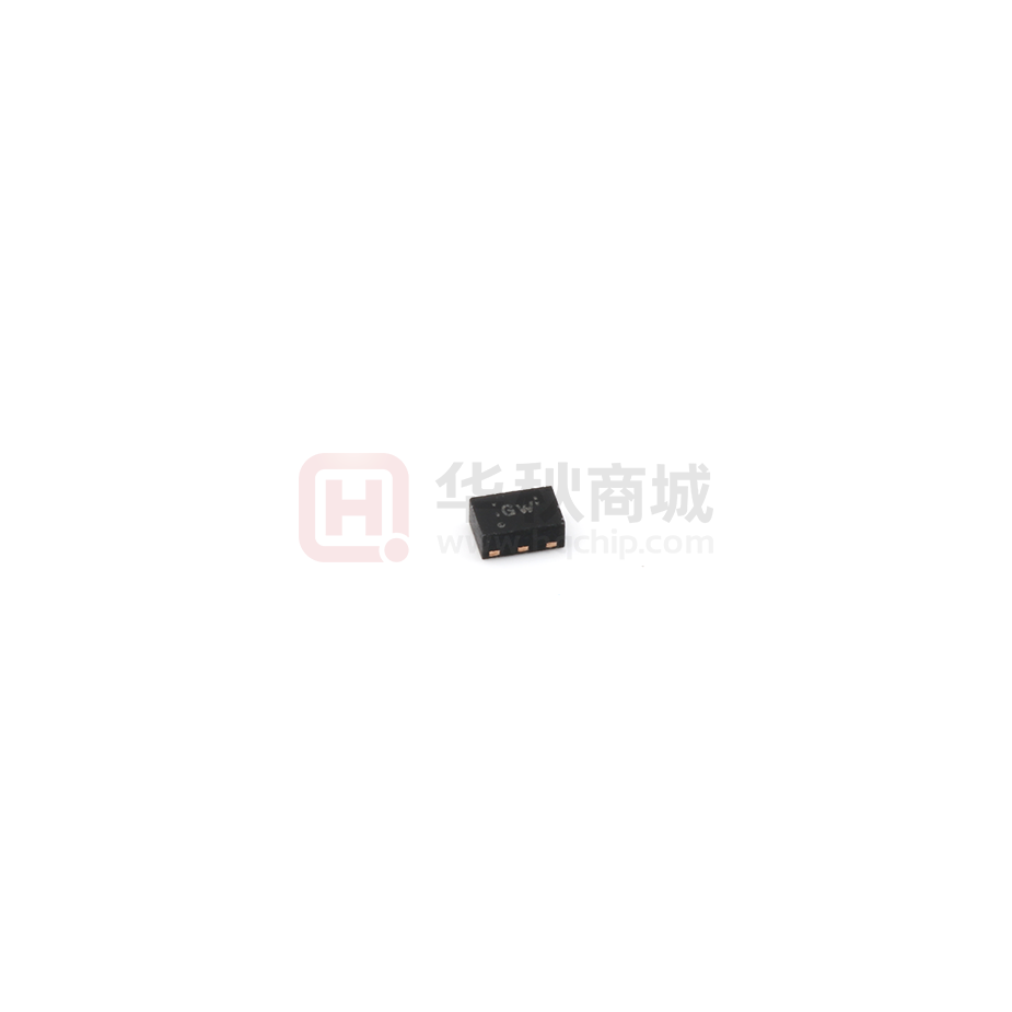


 工商网监
湘ICP备2023018690号
工商网监
湘ICP备2023018690号