Sample &
Buy
Product
Folder
Support &
Community
Tools &
Software
Technical
Documents
Reference
Design
TPS62260, TPS62261, TPS62262, TPS62263
SLVS763E – JUNE 2007 – REVISED JULY 2015
TPS6226x 2.25-MHz 600-mA Step Down Converter in 2 x 2 WSON and SOT Package
1 Features
•
•
•
1
•
•
•
•
•
•
•
•
High Efficiency Step-Down Converter
Output Current up to 600 mA
VIN Range from 2 V to 6 V for Li-ion Batteries with
Extended Voltage Range
2.25-MHz Fixed Frequency Operation
Power Save Mode at Light Load Currents
Output Voltage Accuracy in PWM Mode ±1.5%
Typical 15-μA Quiescent Current
100% Duty Cycle for Lowest Dropout
Voltage Positioning at Light Loads
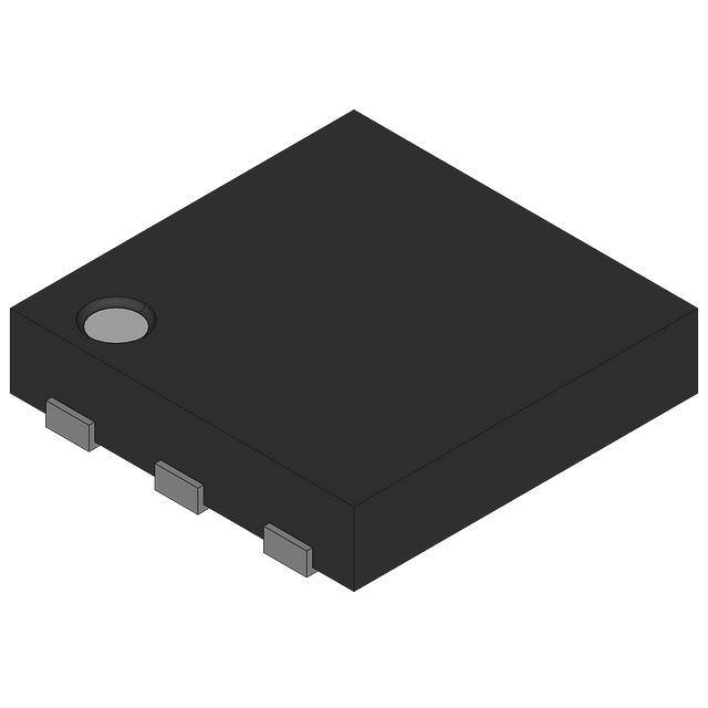
Available in a SOT (5) and 2-mm × 2-mm × 0.8mm WSON (6) Package
Allows 4.5 V. The input capacitor can be increased without any
limit for better input voltage filtering. Take care when using only small ceramic input capacitors. When a ceramic
capacitor is used at the input and the power is being supplied through long wires, such as from a wall adapter, a
load step at the output or VIN step on the input can induce ringing at the VIN pin. This ringing can couple to the
output and be mistaken as loop instability or could even damage the part by exceeding the maximum ratings.
Table 3. List of Capacitors
CAPACITANCE
TYPE
SIZE
SUPPLIER
4.7 μF
GRM188R60J475K
0603 1.6 × 0.8 × 0.8 mm3
Murata
10 μF
GRM188R60J106M69D
0603 1.6 × 0.8 × 0.8 mm3
Murata
Table 1 shows the list of components for the Application Curves.
Copyright © 2007–2015, Texas Instruments Incorporated
Submit Documentation Feedback
Product Folder Links: TPS62260 TPS62261 TPS62262 TPS62263
13
�TPS62260, TPS62261, TPS62262, TPS62263
SLVS763E – JUNE 2007 – REVISED JULY 2015
www.ti.com
9.2.3 Application Curves
100%
100%
VI = 2.3 V
90%
80%
VI = 4.5 V
VI = 3.6 V
60%
50%
VI = 3 V
40%
30%
VO = 1.8 V
MODE = GND
L = 2.2 μH
DCR = 110 mΩ
10%
0%
10μ
40%
VI = 4.5 V
100μ
1m
10m
Output Current (A)
100m
VO = 1.8 V
MODE = VI
L = 2.2 μH
10%
0%
1m
1
10m
100m
Output Current (A)
1
Figure 8. Efficiency (PWM Mode) vs Output Current
100%
100%
90%
90%
VI = 4.2 V
VI = 3.6 V
Efficiency
VI = 5 V
50%
VI = 4.5 V
40%
VO = 3.3 V
MODE = VI
L = 2.2 μH
DCR = 110 mΩ
CO = 10 μF 0603
30%
20%
10%
0%
1m
10m
100m
Output Current (A)
0%
10μ
1
VO = 3.3 V
MODE = GND
L = 2.2 μH
DCR = 110 mΩ
CO = 10 μF 0603
100μ
1m
10m
Output Current (A)
100m
1
Figure 10. Efficiency (Power Save Mode) vs Output
Current
90%
VI = 2.7 V
VI = 2.3 V
80%
VI = 4.5 V
70%
Efficiency
VI = 2.3 V
VI = 4.5 V
VI = 3.6 V
20%
10%
0%
1m
VI = 4.2 V
100%
50%
30%
40%
10%
90%
40%
50%
20%
100%
60%
VI = 4.5 V
60%
30%
Figure 9. Efficiency (PWM Mode) vs Output Current
70%
VI = 5 V
70%
60%
80%
VI = 3.6 V
80%
70%
Efficiency
VI = 3.6 V
50%
20%
Figure 7. Efficiency (Power Save Mode) vs Output Current
Efficiency
VI = 3 V
60%
30%
20%
VO = 1.2 V
MODE = VI
L = 2 μH
MIPSA2520
CO = 10 μF 0603
10m
100m
Output Current (A)
Figure 11. Efficiency vs Output Current
14
VI = 2.7 V
70%
Efficiency
Efficiency
70%
80%
VI = 2.3 V
90%
80% VI = 2.7 V
Submit Documentation Feedback
VI = 3.6 V
60%
50%
VI = 2.7 V
40%
VO = 1.2 V
MODE = GND
L = 2 μH
MIPSA2520
CO = 10 μF 0603
30%
20%
10%
1
0%
10μ
100μ
1m
10m
Output Current (A)
100m
1
Figure 12. Efficiency vs Output Current
Copyright © 2007–2015, Texas Instruments Incorporated
Product Folder Links: TPS62260 TPS62261 TPS62262 TPS62263
�TPS62260, TPS62261, TPS62262, TPS62263
www.ti.com
SLVS763E – JUNE 2007 – REVISED JULY 2015
1.88
1.88
1.86
1.86
PFM Mode, Voltage Positioning
Output Voltage DC (V)
Output Voltage DC (V)
PFM Mode, Voltage Positioning
1.84
1.82
1.80
VI = 2.3 V
VI = 3.6 V
VI = 2.7 V
1.78
1.76
1.74
10μ
100μ
PWM
Mode
VI = 4.5 V
VI = 3 V
TA = 25°C
VO = 1.8 V
MODE = GND
L = 2.2 μH
CO = 10 μF
1m
10m
Output Current (A)
100m
Output Voltage DC (V)
Output Voltage DC (V)
TA = –40°C
VO = 1.8 V
MODE = GND
L = 2.2 μH
CO = 10 μF
1.78
100μ
1m
10m
Output Current (A)
100m
1
1.82
VI = 3.6 V
VI = 2.7 V
1.78
100μ
PWM
Mode
VI = 4.5 V
VI = 3 V
VI = 2 V
TA = 25°C
VO = 1.8 V
MODE = VI
L = 2.2 μH
1.836
1.84
1.76
TA = 85°C
VO = 1.8 V
MODE = GND
L = 2.2 μH
CO = 10 μF
1m
10m
Output Current (A)
100m
1.818
1.8
1.782
VI = 3 V
VI = 2.3 V
VI = 2.7 V
VI = 4.5 V
VI = 3.6 V
1.764
1.746
10μ
1
Figure 15. Output Voltage Accuracy (Power Save Mode) vs
Output Current
100μ
1m
10m
Output Current (A)
100m
1
Figure 16. Output Voltage Accuracy (PWM Mode) vs
Output Current
1.854
1.854
TA = –40°C
VO = 1.8 V
MODE = VI
L = 2.2 μH
1.818
1.8
VI = 2 V
VI = 3 V
VI = 2.7 V
TA = 85°C
VO = 1.8 V
MODE = VI
L = 2.2 μH
1.836
Output Voltage DC (V)
1.836
Output Voltage DC (V)
VI = 2.7 V
PWM
Mode
VI = 3.6 V
1.854
PFM Mode, Voltage Positioning
VI = 4.5 V
VI = 3.6 V
1.764
1.746
10μ
VI = 4.5 V
VI = 3 V
VI = 2.3 V
Figure 14. Output Voltage Accuracy (Power Save Mode) vs
Output Current
1.86
1.782
1.80
1.74
10μ
1
1.88
1.74
10μ
1.82
1.76
Figure 13. Output Voltage Accuracy vs Output Current
1.80
1.84
1.818
1.8
1.782
VI = 2.3 V
VI = 3 V
VI = 2.7 V
VI = 4.5 V
VI = 3.6 V
1.764
100μ
1m
10m
Output Current (A)
100m
1
Figure 17. Output Voltage Accuracy (PWM Mode) vs
Output Current
Copyright © 2007–2015, Texas Instruments Incorporated
1.746
10μ
100μ
1m
10m
Output Current (A)
100m
1
Figure 18. Output Voltage Accuracy (PWM Mode) vs
Output Current
Submit Documentation Feedback
Product Folder Links: TPS62260 TPS62261 TPS62262 TPS62263
15
�TPS62260, TPS62261, TPS62262, TPS62263
SLVS763E – JUNE 2007 – REVISED JULY 2015
VO (10 mV/Div)
www.ti.com
VI = 3.6 V
VO = 1.8 V, IO = 150 mA
L = 2.2 μH, CO = 10 μF 0603
VO (20 mV/Div)
VI = 3.6 V
VO = 1.8 V, IO = 10 mA
L = 2.2 μH, CO = 10 μF
SW (2 V/Div)
SW (2 V/Div)
ICOIL (200 mA/Div)
ICOIL (200 mA/Div)
Time Base (10 μs/Div)
Time Base (10 μs/Div)
Figure 19. Typical Operation (PWM Mode)
VI = 3.6 V
VO = 1.8 V
IO = 10 mA
MODE (2 V/Div)
Figure 20. Typical Operation (PFM Mode)
VI = 3.6 V
VO = 1.8 V
IO = 10 mA
MODE
(2 V/Div)
SW
(2 V/Div)
SW
(2 V/Div)
PFM Mode
Forced PWM Mode
Forced PWM Mode
PFM Mode
ICOIL
(200 mA/Div)
ICOIL
(200 mA/Div)
Time Base (1 μs/Div)
Figure 21. Mode Pin Transition from PFM
to Forced PWM Mode at Light Load
EN
(2 V/Div)
Time Base (2.5 μs/Div)
Figure 22. Mode Pin Transition from PWM
to PFM Mode at Light Load
VI = 3.6 V
VO = 1.5 V
IO = 50 mA to 200 mA
MODE = VIN
VO (50 mV/Div)
SW (2 V/Div)
IO (200 mA/Div)
VO (2 V/Div)
50 mA
ICOIL (500 mA/Div)
II (100 mA/Div)
VI = 3.6 V, RL = 10 Ω
VO = 1.8 V, II into CI
MODE = GND
Time Base (100 μs/Div)
Figure 23. Start-Up Timing
16
200 mA
Submit Documentation Feedback
Time Base (20 μs/Div)
Figure 24. Load Transient (Forced PWM Mode)
Copyright © 2007–2015, Texas Instruments Incorporated
Product Folder Links: TPS62260 TPS62261 TPS62262 TPS62263
�TPS62260, TPS62261, TPS62262, TPS62263
www.ti.com
SLVS763E – JUNE 2007 – REVISED JULY 2015
VI = 3.6 V
VO = 1.5 V
IO = 200 mA to 400 mA
VO (50 mV/Div)
IO (200 mA/Div)
400 mA
SW (2 V/Div)
VI = 3.6 V
VO = 1.5 V
IO = 150 μA to 400 mA
MODE = GND
VO (50 mV/Div)
200 mA
400 mA
IO (500 mA/Div)
ICOIL (500 mA/Div)
150 μA
ICOIL (500 mA/Div)
Time Base (500 μs/Div)
Time Base (20 μs/Div)
Figure 25. Load Transient (Forced PWM Mode)
Figure 26. Load Transient (PFM Mode to PWM Mode)
SW (2 V/Div)
SW (2 V/Div)
VI = 3.6 V
VO = 1.5 V
IO = 150 μA to 400 mA
MODE = GND
VI = 3.6 V
VO = 1.5 V
IO = 1.5 mA to 50 mA
MODE = GND
VO (50 mV/Div)
VO (50 mV/Div)
400 mA
150 μA
50 mA
IO (50 mA/Div)
IO (500 mA/Div)
1.5 mA
ICOIL (500 mA/Div)
ICOIL (500 mA/Div)
Time Base (50 μs/Div)
Time Base (500 μs/Div)
Figure 27. Load Transient (PWM Mode to PFM Mode)
Figure 28. Load Transient (PFM Mode)
SW (2 V/Div)
SW (2 V/Div)
VO (50 mV/Div)
50 mA
VI = 3.6 V
VO = 1.5 V
IO = 50 mA to 1.5 mA
MODE = GND
VO (50 mV/Div)
VI = 3.6 V
VO = 1.8 V
IO = 50 mA to 250 mA
MODE = GND
IO (50 mA/Div)
1.5 mA
50 mA
250 mA
IO (200 mA/Div)
ICOIL (500 mA/Div)
ICOIL (500 mA/Div)
Time Base (50 μs/Div)
Figure 29. Load Transient (PFM Mode)
Copyright © 2007–2015, Texas Instruments Incorporated
Time Base (20 μs/Div)
Figure 30. Load Transient (PFM Mode to PWM Mode)
Submit Documentation Feedback
Product Folder Links: TPS62260 TPS62261 TPS62262 TPS62263
17
�TPS62260, TPS62261, TPS62262, TPS62263
SLVS763E – JUNE 2007 – REVISED JULY 2015
www.ti.com
SW (2 V/Div)
VO (50 mV/Div)
PFM Mode
IO (500 mA/Div)
50 mA
VI = 3.6 V
VO = 1.5 V
IO = 50 mA to 400 mA
MODE = GND
PWM Mode
400 mA
ICOIL (500 mA/Div)
Time Base (20 μs/Div)
Figure 31. Load Transient (PFM Mode to PWM Mode)
VI = 3.6 V to 4.2 V
(500 mV/Div)
VI = 3.6 V to 4.2 V
(500 mV/Div)
VO = 1.8 V
(50 mV/Div)
IO = 50 mA
MODE = GND
VO = 1.8 V
(50 mV/Div)
IO = 250 mA
MODE = VIN
Time Base (100 μs/Div)
Figure 33. Line Transient (PFM Mode)
18
Figure 32. Load Transient (PWM Mode to PFM Mode)
Submit Documentation Feedback
Time Base (100 μs/Div)
Figure 34. Line Transient (Forced PWM Mode)
Copyright © 2007–2015, Texas Instruments Incorporated
Product Folder Links: TPS62260 TPS62261 TPS62262 TPS62263
�TPS62260, TPS62261, TPS62262, TPS62263
www.ti.com
SLVS763E – JUNE 2007 – REVISED JULY 2015
9.3 System Examples
9.3.1 TPS62260, Adjustable 1.5-V Output
TPS62260DRV
VIN
CIN
4.7 mF
VOUT 1.5 V
Up to 600 mA
L1
2.2 mH
VIN = 2 V to 6 V
SW
R1
540 kΩ
EN
C1
22 pF
COUT
10 mF
FB
GND
R2
360 kΩ
MODE
Figure 35. TPS62260 Adjustable 1.5-V Output
9.3.2 TPS62262, Fixed 1.2-V Output
TPS62262DRV
VIN = 2 V to 6 V
VIN
CIN
4.7 mF
L1
2.2 mH
VOUT 1.2 V
Up to 600 mA
SW
COUT
10 mF
EN
FB
GND
MODE
Figure 36. TPS62262 Fixed 1.2-V Output
9.3.3 TPS62261, Fixed 1.8-V Output
L1
2.2 mH
TPS62261DRV
VIN = 2 V to 6 V
VIN
CIN
4.7 mF
VOUT 1.8 V
Up to 600 mA
SW
EN
FB
GND
COUT
10 mF
MODE
Figure 37. TPS62261 Fixed 1.8-V Output
Copyright © 2007–2015, Texas Instruments Incorporated
Submit Documentation Feedback
Product Folder Links: TPS62260 TPS62261 TPS62262 TPS62263
19
�TPS62260, TPS62261, TPS62262, TPS62263
SLVS763E – JUNE 2007 – REVISED JULY 2015
www.ti.com
10 Power Supply Recommendations
The TPS6226x device has no special requirements for its input power supply. The input power supply output
current must be rated according to the supply voltage, output voltage, and output current of the TPS6226x.
11 Layout
11.1 Layout Guidelines
As for all switching power supplies, the layout is an important step in the design. Proper function of the device
demands careful attention to PCB layout. Care must be taken in board layout to get the specified performance. If
the layout is not carefully done, the regulator could show poor line and/or load regulation, and additional stability
issues as well as EMI problems. It is critical to provide a low inductance, impedance ground path. Therefore, use
wide and short traces for the main current paths. The input capacitor should be placed as close as possible to
the IC pins as well as the inductor and output capacitor.
Connect the GND pin of the device to the PowerPAD™ land of the PCB and use this pad as a star point. Use a
common power GND node and a different node for the signal GND to minimize the effects of ground noise.
Connect these ground nodes together to the PowerPAD land (star point) underneath the IC. Keep the common
path to the GND pin, which returns the small signal components and the high current of the output capacitors as
short as possible to avoid ground noise. The FB line should be connected right to the output capacitor and routed
away from noisy components and traces (for example, the SW line).
11.2 Layout Examples
Figure 38. Suggested Layout for Fixed Output Voltage Options
20
Submit Documentation Feedback
Copyright © 2007–2015, Texas Instruments Incorporated
Product Folder Links: TPS62260 TPS62261 TPS62262 TPS62263
�TPS62260, TPS62261, TPS62262, TPS62263
www.ti.com
SLVS763E – JUNE 2007 – REVISED JULY 2015
Layout Examples (continued)
VOUT
R2
GND
C1
R1
COUT
CIN
VIN
L
G
N
D
U
Figure 39. Suggested Layout for Adjustable Output Voltage Version
Copyright © 2007–2015, Texas Instruments Incorporated
Submit Documentation Feedback
Product Folder Links: TPS62260 TPS62261 TPS62262 TPS62263
21
�TPS62260, TPS62261, TPS62262, TPS62263
SLVS763E – JUNE 2007 – REVISED JULY 2015
www.ti.com
12 Device and Documentation Support
12.1 Device Support
12.1.1 Third-Party Products Disclaimer
TI'S PUBLICATION OF INFORMATION REGARDING THIRD-PARTY PRODUCTS OR SERVICES DOES NOT
CONSTITUTE AN ENDORSEMENT REGARDING THE SUITABILITY OF SUCH PRODUCTS OR SERVICES
OR A WARRANTY, REPRESENTATION OR ENDORSEMENT OF SUCH PRODUCTS OR SERVICES, EITHER
ALONE OR IN COMBINATION WITH ANY TI PRODUCT OR SERVICE.
12.2 Related Links
The table below lists quick access links. Categories include technical documents, support and community
resources, tools and software, and quick access to sample or buy.
Table 4. Related Links
PARTS
PRODUCT FOLDER
SAMPLE & BUY
TECHNICAL
DOCUMENTS
TOOLS &
SOFTWARE
SUPPORT &
COMMUNITY
TPS62260
Click here
Click here
Click here
Click here
Click here
TPS62261
Click here
Click here
Click here
Click here
Click here
TPS62262
Click here
Click here
Click here
Click here
Click here
TPS62263
Click here
Click here
Click here
Click here
Click here
12.3 Community Resources
The following links connect to TI community resources. Linked contents are provided "AS IS" by the respective
contributors. They do not constitute TI specifications and do not necessarily reflect TI's views; see TI's Terms of
Use.
TI E2E™ Online Community TI's Engineer-to-Engineer (E2E) Community. Created to foster collaboration
among engineers. At e2e.ti.com, you can ask questions, share knowledge, explore ideas and help
solve problems with fellow engineers.
Design Support TI's Design Support Quickly find helpful E2E forums along with design support tools and
contact information for technical support.
12.4 Trademarks
PowerPAD, E2E are trademarks of Texas Instruments.
All other trademarks are the property of their respective owners.
12.5 Electrostatic Discharge Caution
These devices have limited built-in ESD protection. The leads should be shorted together or the device placed in conductive foam
during storage or handling to prevent electrostatic damage to the MOS gates.
12.6 Glossary
SLYZ022 — TI Glossary.
This glossary lists and explains terms, acronyms, and definitions.
13 Mechanical, Packaging, and Orderable Information
The following pages include mechanical, packaging, and orderable information. This information is the most
current data available for the designated devices. This data is subject to change without notice and revision of
this document. For browser-based versions of this data sheet, refer to the left-hand navigation.
22
Submit Documentation Feedback
Copyright © 2007–2015, Texas Instruments Incorporated
Product Folder Links: TPS62260 TPS62261 TPS62262 TPS62263
�PACKAGE OPTION ADDENDUM
www.ti.com
14-Oct-2022
PACKAGING INFORMATION
Orderable Device
Status
(1)
Package Type Package Pins Package
Drawing
Qty
Eco Plan
(2)
Lead finish/
Ball material
MSL Peak Temp
Op Temp (°C)
Device Marking
(3)
Samples
(4/5)
(6)
TPS62260DDCR
ACTIVE
SOT-23-THIN
DDC
5
3000
RoHS & Green
NIPDAU
Level-1-260C-UNLIM
-40 to 85
BYP
Samples
TPS62260DDCT
ACTIVE
SOT-23-THIN
DDC
5
250
RoHS & Green
NIPDAU
Level-1-260C-UNLIM
-40 to 85
BYP
Samples
TPS62260DDCTG4
ACTIVE
SOT-23-THIN
DDC
5
250
RoHS & Green
NIPDAU
Level-1-260C-UNLIM
-40 to 85
BYP
Samples
TPS62260DRVR
ACTIVE
WSON
DRV
6
3000
RoHS & Green
NIPDAUAG
Level-1-260C-UNLIM
-40 to 85
BYK
Samples
TPS62260DRVT
ACTIVE
WSON
DRV
6
250
RoHS & Green
NIPDAUAG
Level-1-260C-UNLIM
-40 to 85
BYK
Samples
TPS62260DRVTG4
ACTIVE
WSON
DRV
6
250
RoHS & Green
NIPDAUAG
Level-1-260C-UNLIM
-40 to 85
BYK
Samples
TPS62261DRVR
ACTIVE
WSON
DRV
6
3000
RoHS & Green
NIPDAU
Level-1-260C-UNLIM
-40 to 85
BYL
Samples
TPS62261DRVT
ACTIVE
WSON
DRV
6
250
RoHS & Green
NIPDAU
Level-1-260C-UNLIM
-40 to 85
BYL
Samples
TPS62262DDCR
ACTIVE
SOT-23-THIN
DDC
5
3000
RoHS & Green
NIPDAU
Level-1-260C-UNLIM
-40 to 85
QXS
Samples
TPS62262DDCT
ACTIVE
SOT-23-THIN
DDC
5
250
RoHS & Green
NIPDAU
Level-1-260C-UNLIM
-40 to 85
QXS
Samples
TPS62262DRVR
ACTIVE
WSON
DRV
6
3000
RoHS & Green
NIPDAUAG
Level-1-260C-UNLIM
-40 to 85
BYM
Samples
TPS62262DRVT
ACTIVE
WSON
DRV
6
250
RoHS & Green
NIPDAUAG
Level-1-260C-UNLIM
-40 to 85
BYM
Samples
TPS62263DRVR
ACTIVE
WSON
DRV
6
3000
RoHS & Green
NIPDAU
Level-1-260C-UNLIM
-40 to 85
CFX
Samples
TPS62263DRVT
ACTIVE
WSON
DRV
6
250
RoHS & Green
NIPDAU
Level-1-260C-UNLIM
-40 to 85
CFX
Samples
(1)
The marketing status values are defined as follows:
ACTIVE: Product device recommended for new designs.
LIFEBUY: TI has announced that the device will be discontinued, and a lifetime-buy period is in effect.
NRND: Not recommended for new designs. Device is in production to support existing customers, but TI does not recommend using this part in a new design.
PREVIEW: Device has been announced but is not in production. Samples may or may not be available.
OBSOLETE: TI has discontinued the production of the device.
(2)
RoHS: TI defines "RoHS" to mean semiconductor products that are compliant with the current EU RoHS requirements for all 10 RoHS substances, including the requirement that RoHS substance
do not exceed 0.1% by weight in homogeneous materials. Where designed to be soldered at high temperatures, "RoHS" products are suitable for use in specified lead-free processes. TI may
reference these types of products as "Pb-Free".
Addendum-Page 1
�PACKAGE OPTION ADDENDUM
www.ti.com
14-Oct-2022
RoHS Exempt: TI defines "RoHS Exempt" to mean products that contain lead but are compliant with EU RoHS pursuant to a specific EU RoHS exemption.
Green: TI defines "Green" to mean the content of Chlorine (Cl) and Bromine (Br) based flame retardants meet JS709B low halogen requirements of