Order
Now
Product
Folder
Support &
Community
Tools &
Software
Technical
Documents
TPS6283810
SLVSEX7 – DECEMBER 2018
TPS6283810, Tiny 6-pin 3-A Step-Down Converter in 1.2-mm x 0.8-mm WCSP
1 Features
3 Description
•
•
•
•
•
•
•
•
•
•
•
•
•
The device is a high-frequency synchronous stepdown converter optimized for small solution size and
high efficiency. With an input voltage range of 2.4 V
to 5.5 V, common battery technologies are supported.
At medium to heavy loads, the converter operates in
PWM mode and automatically enters Power Save
Mode operation at light load to maintain high
efficiency over the entire load current range. The 3.5MHz switching frequency allows the device to use
small external components. Together with its DCScontrol architecture, excellent load transient
performance and output voltage regulation accuracy
are achieved. Other features like over current
protection, thermal shutdown protection, active output
discharge and power good are built-in. The device is
available in a 6-pin WCSP package.
1
DCS-Control™ Topology
1-V Fixed Output Voltage, with 1% Accuracy
26mΩ and 26mΩ Internal Power MOSFETs
2.4-V to 5.5-V Input Voltage Range
4-μA Operating Quiescent Current
3.5-MHz Switching Frequency
Power Save Mode for Light Load Efficiency
Active Output Discharge
Power Good Output
Thermal Shutdown Protection
Hiccup Short-Circuit Protection
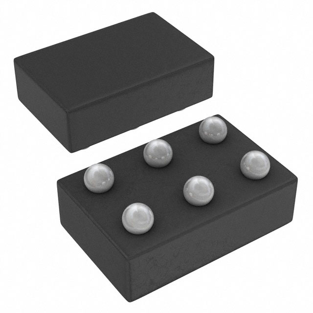
Available in 0.8 x 1.2 x 0.5-mm 6-Pin WCSP
Create a Custom Design Using the TPS6283810
With the WEBENCH® Power Designer
PART NUMBER
2 Applications
•
•
•
•
Device Information(1)
TPS6283810
Consumer Wireless Modules
Wearable Products
Smart Phones
Optical Modules
PACKAGE
BODY SIZE (NOM)
YFP (6)
1.2mm x 0.8mm
(1) For all available packages, see the orderable addendum at
the end of the data sheet.
Spacer
Typical Application Schematic
TPS6283810
VIN
R3
100 k
C1
4.7 µF
EN
Efficiency
VOUT
1.0 V
L1
0.24 µH
100
SW
FB
C2
10 µF
95
C3
10 µF
90
85
VPG
PG GND
Copyright Ú 2018, Texas Instruments Incorporated
Efficiency (%)
VIN
2.4 V to 5.5 V
80
75
70
65
60
55
50
100P
VIN = 2.5V
VIN = 3.3V
VIN = 4.2V
VIN = 5.0V
1m
10m
Load (A)
100m
1
3
D003
1
An IMPORTANT NOTICE at the end of this data sheet addresses availability, warranty, changes, use in safety-critical applications,
intellectual property matters and other important disclaimers. PRODUCTION DATA.
�TPS6283810
SLVSEX7 – DECEMBER 2018
www.ti.com
Table of Contents
1
2
3
4
5
6
7
Features ..................................................................
Applications ...........................................................
Description .............................................................
Revision History.....................................................
Pin Configuration and Functions .........................
Specifications.........................................................
1
1
1
2
3
4
6.1
6.2
6.3
6.4
6.5
6.6
4
4
4
4
4
6
Absolute Maximum Ratings ......................................
ESD Ratings..............................................................
Recommended Operating Conditions.......................
Thermal Information ..................................................
ELECTRICAL CHARACTERISTICS ........................
Typical Characteristics ..............................................
Detailed Description .............................................. 7
7.1
7.2
7.3
7.4
Overview ...................................................................
Functional Block Diagram .........................................
Feature Description...................................................
Device Functional Modes..........................................
7
7
7
9
8
Application and Implementation ........................ 10
8.1 Application Information............................................ 10
8.2 Typical Application ................................................. 10
9 Power Supply Recommendations...................... 15
10 Layout................................................................... 15
10.1 Layout Guidelines ................................................. 15
10.2 Layout Example .................................................... 15
10.3 Thermal Considerations ........................................ 15
11 Device and Documentation Support ................. 16
11.1
11.2
11.3
11.4
11.5
11.6
Device Support......................................................
Documentation Support ........................................
Community Resources..........................................
Trademarks ...........................................................
Electrostatic Discharge Caution ............................
Glossary ................................................................
16
16
16
16
16
16
12 Mechanical, Packaging, and Orderable
Information ........................................................... 17
4 Revision History
NOTE: Page numbers for previous revisions may differ from page numbers in the current version.
2
DATE
REVISION
NOTES
December 2018
*
Initial release
Submit Documentation Feedback
Copyright © 2018, Texas Instruments Incorporated
Product Folder Links: TPS6283810
�TPS6283810
www.ti.com
SLVSEX7 – DECEMBER 2018
5 Pin Configuration and Functions
YFP Package
Top View
YFP Package
Bottom View
1
A
2
EN
C
FB
GND
B
PG
SW
A
EN
VIN
SW
FB
C
2
VIN
PG
B
1
GND
Not to scale
Not to scale
Pin Functions
PIN
I/O
DESCRIPTION
A1
I
Device enable pin. To enable the device, this pin needs to be pulled high. Pulling this pin low
disables the device. Do not leave floating.
PG
B1
O
Power good open drain output pin. The pull-up resistor can be connected to voltages up to
5.5 V. If unused, leave it floating.
FB
C1
I
Feedback pin. For the fixed output voltage versions, this pin must be connected to the
output.
GND
C2
SW
B2
PWR
Switch pin of the power stage.
VIN
A2
PWR
Input voltage pin.
NAME
NO.
EN
Ground pin.
Submit Documentation Feedback
Copyright © 2018, Texas Instruments Incorporated
Product Folder Links: TPS6283810
3
�TPS6283810
SLVSEX7 – DECEMBER 2018
www.ti.com
6 Specifications
6.1 Absolute Maximum Ratings (1)
Voltage at Pins (2)
Temperature
(1)
(2)
(3)
MIN
MAX
VIN, FB, EN, PG
–0.3
6
SW (DC)
–0.3
VIN + 0.3
SW (DC, in current limit)
-1.0
VIN + 0.3
SW (AC, less than 10ns) (3)
-2.5
10
Operating Junction, TJ
–40
150
Storage, Tstg
–65
150
UNIT
V
°C
Stresses beyond those listed under Absolute Maximum Ratings may cause permanent damage to the device. These are stress ratings
only and functional operation of the device at these or any other conditions beyond those indicated under Recommended Operating
Conditions is not implied. Exposure to absolute–maximum–rated conditions for extended periods may affect device reliability.
All voltage values are with respect to network ground terminal.
While switching
6.2 ESD Ratings
VALUE
V(ESD)
(1)
(2)
Electrostatic discharge
Human body model (HBM), per ANSI/ESDA/JEDEC JS-001 (1)
±2000
Charged device model (CDM), per JEDEC specification JESD22-C101 (2)
±500
UNIT
V
JEDEC document JEP155 states that 500-V HBM allows safe manufacturing with a standard ESD control process.
JEDEC document JEP157 states that 250-V CDM allows safe manufacturing with a standard ESD control process.
6.3 Recommended Operating Conditions
MIN NOM
MAX
UNIT
VIN
Input voltage range
2.4
5.5
V
VOUT
Output voltage range
0.6
4
V
IOUT
Output current range (1)
0
3
A
1
mA
ISINK_PG Sink current at PG pin
VPG
Pull-up resistor voltage
TJ
Operating junction temperature
(1)
–40
5.5
V
125
°C
Lifetime is reduced when operating continuously at IOUT = 3 A and the junction temperature ≥ 105 °C.
6.4 Thermal Information
THERMAL METRIC (1)
TPS6283810
YFP (6-PINS), JEDEC
UNIT
RθJA
Junction-to-ambient thermal resistance
141.3
°C/W
RθJC(top)
Junction-to-case (top) thermal resistance
1.7
°C/W
RθJB
Junction-to-board thermal resistance
47.3
°C/W
ψJT
Junction-to-top characterization parameter
0.5
°C/W
ψJB
Junction-to-board characterization parameter
47.5
°C/W
RθJC(bot)
Junction-to-case (bottom) thermal resistance
n/a
°C/W
(1)
6.5
For more information about traditional and new thermal metrics, see the Semiconductor and IC Package Thermal Metrics application
report.
ELECTRICAL CHARACTERISTICS
TJ = -40 °C to 125 °C, and VIN = 2.4 V to 5.5 V. Typical values are at TJ = 25 °C and VIN = 5 V , unless otherwise noted.
PARAMETER
TEST CONDITIONS
MIN
TYP
MAX
UNIT
4
10
µA
0.05
0.5
µA
SUPPLY
IQ
Quiescent current
EN = High, no load, device not switching
ISD
Shutdown current
EN = Low, TJ = -40℃ to 85℃
4
Submit Documentation Feedback
Copyright © 2018, Texas Instruments Incorporated
Product Folder Links: TPS6283810
�TPS6283810
www.ti.com
SLVSEX7 – DECEMBER 2018
ELECTRICAL CHARACTERISTICS (continued)
TJ = -40 °C to 125 °C, and VIN = 2.4 V to 5.5 V. Typical values are at TJ = 25 °C and VIN = 5 V , unless otherwise noted.
PARAMETER
VUVLO
TJSD
TEST CONDITIONS
MIN
2.1
TYP
MAX
2.2
2.3
UNIT
Under voltage lock out threshold
VIN falling
Under voltage lock out hysteresis
VIN rising
160
mV
V
Thermal shutdown threshold
TJ rising
150
°C
Thermal shutdown hysteresis
TJ falling
20
°C
LOGIC INTERFACE EN
VIH
High-level threshold voltage
VIL
Low-level threshold voltage
IEN,LKG
Input leakage current into EN pin
1.0
V
0.01
0.4
V
0.1
µA
SOFT START, POWER GOOD
tSS
Soft start time
Power good lower threshold
VPG
Power good upper threshold
Time from EN high to 95% of VOUT nominal
1.25
ms
VPG rising, VFB referenced to VOUT nominal
94
96
98
%
VPG falling, VFB referenced to VOUT nominal
90
92
94
%
VPG rising, VFB referenced to VOUT nominal
103
105
107
%
VPG falling, VFB referenced to VOUT nominal
108
110
112
%
VPG,OL
Low-level output voltage
Isink = 1 mA
IPG,LKG
Input leakage current into PG pin
VPG = 5.0 V
VOUT
Output voltage accuracy
TPS6283810, PWM mode
RFB
Internal resistor divider connected to FB
pin
IDIS
Output discharge current
0.4
V
0.01
0.1
µA
1.0
1.010
V
OUTPUT
0.990
7.5
MΩ
400
mA
High-side FET on-resistance
26
mΩ
Low-side FET on-resistance
26
mΩ
VSW = 0.4V; EN = LOW
75
POWER SWITCH
RDS(on)
ILIM
High-side FET switch current limit
fSW
PWM switching frequency
3.6
IOUT = 1 A, VOUT = 1.0 V
4.3
5.0
3.5
Submit Documentation Feedback
Copyright © 2018, Texas Instruments Incorporated
Product Folder Links: TPS6283810
A
MHz
5
�TPS6283810
SLVSEX7 – DECEMBER 2018
www.ti.com
70.0
70.0
60.0
60.0
50.0
50.0
RDS(on) (mOhm)
RDS(on) (mOhm)
6.6 Typical Characteristics
40.0
30.0
20.0
10.0
0.0
2.5
40.0
30.0
20.0
TJ = 0 °C
TJ = 25 °C
TJ = 85 °C
TJ = 125 °C
3.0
10.0
3.5
4.0
4.5
Input Voltage (V)
5.0
TJ = 0 °C
TJ = 25 °C
TJ = 85 °C
TJ = 125 °C
0.0
2.5
5.5
3.0
$
6KXWGRZQ &XUUHQW
4XLHVFHQW &XUUHQW
$
0.4
5.5
D011
4.0
TJ = -40 °C
TJ = 25 °C
TJ = 85 °C
TJ = 125 °C
3.0
TJ = -40 °C
TJ = 25 °C
TJ = 85 °C
TJ = 125 °C
0.3
0.2
0.1
3.5
4.0
4.5
Input Voltage (V)
5.0
5.5
0.0
2.5
D001
Figure 3. Quiescent Current
6
5.0
0.5
6.0
0.0
2.5
4.0
4.5
Input Voltage (V)
Figure 2. Low-Side FET On-Resistance
Figure 1. High-Side FET On-Resistance
8.0
2.0
3.5
D010
3.0
3.5
4.0
4.5
Input Voltage (V)
5.0
5.5
D000
Figure 4. Shutdown Current
Submit Documentation Feedback
Copyright © 2018, Texas Instruments Incorporated
Product Folder Links: TPS6283810
�TPS6283810
www.ti.com
SLVSEX7 – DECEMBER 2018
7 Detailed Description
7.1 Overview
The synchronous step-down converter adopts a DCS-Control (Direct Control with Seamless transition into Power
Save Mode) topology. This is an advanced regulation topology that combines the advantages of hysteretic,
voltage, and current mode control schemes.
The DCS-Control topology operates in PWM (pulse width modulation) mode for medium to heavy load conditions
and in Power Save Mode at light load currents. In PWM mode, the converter operates with its nominal switching
frequency of 3.5 MHz, having a controlled frequency variation over the input voltage range. As the load current
decreases, the converter enters Power Save Mode, reducing the switching frequency and minimizing the IC
current consumption to achieve high efficiency over the entire load current range. Because DCS-Control supports
both operation modes (PWM and PFM) within a single building block, the transition from PWM mode to Power
Save Mode is seamless and without effects on the output voltage. The devices offer both excellent DC voltage
and superior load transient regulation, combined with very low output voltage ripple, minimizing interference with
RF circuits.
7.2 Functional Block Diagram
PG
VPG_H
Control Logic
VREF
UVLO
Thermal Shutdown
Startup
EN
VIN
+
±
VFB
VPG_L
+
±
GND
Peak Current Detect
VSW
TON
VIN
VSW
HICCUP
Direct Control
&
Compensation
VREF
Modulator
Comparator
FB
Zero Current Detect
Discharge
+
_EA
SW
Gate
Drive
GND
Fixed VOUT
GND
7.3 Feature Description
7.3.1 Power Save Mode
As the load current decreases, the device enters Power Save Mode (PSM) operation. The power save mode
occurs when the inductor current becomes discontinuous. PSM is based on a fixed on-time architecture and the
switching frequency in PSM is reduced, as related in Equation 1.
Submit Documentation Feedback
Copyright © 2018, Texas Instruments Incorporated
Product Folder Links: TPS6283810
7
�TPS6283810
SLVSEX7 – DECEMBER 2018
www.ti.com
Feature Description (continued)
t ON
250ns u
VOUT
VIN
2 u IOUT
V
VOUT
V
2
u IN u IN
t ON
VOUT
L
fPSM
(1)
In Power Save Mode, the output voltage rises slightly above the nominal output voltage. This effect is minimized
by increasing the output capacitor or inductor value.
When the device operates close to 100% duty cycle mode, the device can't enter Power Save Mode regardless
of the load current if the input voltage decreases to typically 10% above the output voltage. The device maintains
output regulation in PWM mode.
7.3.2 100% Duty Cycle Low Dropout Operation
The devices offer low input-to-output voltage difference by entering 100% duty cycle mode. In this mode, the
high-side MOSFET switch is constantly turned on and the low-side MOSFET is switched off. This is particularly
useful in battery powered applications to achieve the longest operation time by taking full advantage of the whole
battery voltage range. The minimum input voltage to maintain output regulation, depending on the load current
and output voltage can be calculated as:
VIN,MIN = VOUT + IOUT,MAX ´ (RDS(on) + RL )
where
•
•
•
•
VIN,MIN = Minimum input voltage to maintain an output voltage
IOUT,MAX = Maximum output current
RDS(on) = High-side FET ON-resistance
RL = Inductor ohmic resistance (DCR)
(2)
7.3.3 Soft Start
After enabling the device, there is a 250-µs delay before switching starts. Then, an internal soft startup circuitry
ramps up the output voltage which reaches nominal output voltage during the startup time of 1 ms. This avoids
excessive inrush current and creates a smooth output voltage rise slope. It also prevents excessive voltage
drops of primary cells and rechargeable batteries with high internal impedance.
The device is able to start into a pre-biased output capacitor. It starts with the applied bias voltage and ramps the
output voltage to its nominal value.
7.3.4 Switch Current Limit and HICCUP Short-Circuit Protection
The switch current limit prevents the device from high inductor current and from drawing excessive current from
the battery or input voltage rail. Excessive current might occur with a shorted or saturated inductor or a heavy
load or shorted output circuit condition. If the inductor current reaches the threshold ILIM, the high-side MOSFET
is turned off and the low-side MOSFET remains off, while the inductor current flows through its body diode and
quickly ramps down.
When this switch current limits is triggered 32 times, the device stops switching. The device then automatically
starts a new start-up after a typical delay time of 128 µs has passed. This is named HICCUP short-circuit
protection. The device repeats this mode until the high load condition disappears.
7.3.5 Undervoltage Lockout
To avoid mis-operation of the device at low input voltages, under voltage lockout is implemented that shuts down
the device at voltages lower than VUVLO.
8
Submit Documentation Feedback
Copyright © 2018, Texas Instruments Incorporated
Product Folder Links: TPS6283810
�TPS6283810
www.ti.com
SLVSEX7 – DECEMBER 2018
Feature Description (continued)
7.3.6 Thermal Shutdown
The device goes into thermal shutdown and stops the power stage switching when the junction temperature
exceeds TJSD. When the device temperature falls below the threshold by 20°C, the device returns to normal
operation automatically by switching the power stage again.
7.4 Device Functional Modes
7.4.1 Enable and Disable
The device is enabled by setting the EN pin to a logic High. Accordingly, shutdown mode is forced if the EN pin
is pulled Low with a shutdown current of typically 50 nA. In shutdown mode, the internal power switches as well
as the entire control circuitry are turned off. An internal switch smoothly discharges the output through the SW
pin in shutdown mode. Do not leave the EN pin floating.
The typical threshold value of the EN pin is 0.89 V for rising input signal, and 0.62 V for falling input signal.
7.4.2 Power Good
The device has a power good output. The PG pin goes high impedance once the FB pin voltage is above 96%
and less than 105% of the nominal voltage, and is driven low once the voltage falls below typically 92% or higher
than 110% of the nominal voltage. The PG pin is an open-drain output and is specified to sink up to 1 mA. The
power good output requires a pull-up resistor connecting to any voltage rail less than 5.5 V. The PG signal can
be used for sequencing of multiple rails by connecting it to the EN pin of other converters. Leave the PG pin
unconnected when not used.
The PG rising edge has a 100-µs blanking time and the PG falling edge has a deglitch delay of 20 µs.
Table 1. PG Pin Logic
DEVICE CONDITIONS
EN = High, VFB ≥ 96% of Nominal Value
Enable
LOGIC STATUS
HIGH IMPEDANCE
EN = High, VFB ≤ 92% of Nominal Value
EN = High, VFB ≤ 105% of Nominal Value
LOW
√
√
√
EN = High, VFB ≥ 110% of Nominal Value
√
Shutdown
EN = Low
√
Thermal Shutdown
TJ > TJSD
√
UVLO
0.7 V < VIN < VUVLO
Power Supply Removal
VIN < 0.7 V
√
√
Submit Documentation Feedback
Copyright © 2018, Texas Instruments Incorporated
Product Folder Links: TPS6283810
9
�TPS6283810
SLVSEX7 – DECEMBER 2018
www.ti.com
8 Application and Implementation
NOTE
Information in the following applications sections is not part of the TI component
specification, and TI does not warrant its accuracy or completeness. TI’s customers are
responsible for determining suitability of components for their purposes. Customers should
validate and test their design implementation to confirm system functionality.
8.1 Application Information
The following section discusses the design of the external components to complete the power supply design for
several input and output voltage options by using typical applications as a reference.
8.2 Typical Application
VIN
2.4 V to 5.5 V
TPS6283810
R3
100 k
C1
4.7 µF
VIN
SW
EN
FB
VOUT
1.0 V
L1
0.24 µH
C2
10 µF
C3
10 µF
VPG
PG GND
Copyright Ú 2018, Texas Instruments Incorporated
Figure 5. Typical Application of Fixed Output
8.2.1 Design Requirements
For this design example, use the parameters listed in Table 2 as the input parameters.
Table 2. Design Parameters
DESIGN PARAMETER
EXAMPLE VALUE
Input voltage
2.4 V to 5.5 V
Output voltage
1.0 V
Maximum peak output current
3A
Table 3 lists the components used for the example.
Table 3. List of Components of Figure 5
REFERENCE
C1
C2, C3
(1)
MANUFACTURER (1)
DESCRIPTION
4.7 µF, Ceramic capacitor, 6.3 V, X7R, size 0603, JMK107BB7475MA
Taiyo Yuden
10 µF, Ceramic capacitor, 10 V, X7R, size 0603, GRM188Z71A106MA73D
Murata
L1
0.24 µH, Power Inductor, size 0603, DFE160810S-R24M (DFE18SANR24MG0)
Murata
R3
100 kΩ, Chip resistor, 1/16 W, 1%, size 0603
Std
See Third-party Products disclaimer.
Table 4. List of Components of Figure 5, Smallest Solution
REFERENCE
C1, C2, C3
MANUFACTURER (1)
DESCRIPTION
10 µF, Ceramic capacitor, 6.3 V, X5R, size 0402, GRM155R60J106ME47
Murata
L1
0.24 µH, Power Inductor, size 0603, DFE160810S-R24M (DFE18SANR24MG0)
Murata
R3
100 kΩ, Chip resistor, 1/16 W, size 0402
(1)
See Third-party Products disclaimer.
10
Submit Documentation Feedback
Std
Copyright © 2018, Texas Instruments Incorporated
Product Folder Links: TPS6283810
�TPS6283810
www.ti.com
SLVSEX7 – DECEMBER 2018
8.2.2 Detailed Design Procedure
8.2.2.1 Custom Design With WEBENCH® Tools
Click here to create a custom design using the device with the WEBENCH® Power Designer.
1. Start by entering the input voltage (VIN), output voltage (VOUT), and output current (IOUT) requirements.
2. Optimize the design for key parameters such as efficiency, footprint, and cost using the optimizer dial.
3. Compare the generated design with other possible solutions from Texas Instruments.
The WEBENCH Power Designer provides a customized schematic along with a list of materials with real-time
pricing and component availability.
In most cases, these actions are available:
• Run electrical simulations to see important waveforms and circuit performance
• Run thermal simulations to understand board thermal performance
• Export customized schematic and layout into popular CAD formats
• Print PDF reports for the design, and share the design with colleagues
Get more information about WEBENCH tools at www.ti.com/WEBENCH.
8.2.2.2 Output Filter Design
The inductor and the output capacitor together provide a low-pass filter. To simplify this process, Table 5 outlines
possible inductor and capacitor value combinations for most applications. Checked cells represent combinations
that are proven for stability by simulation and lab test. Further combinations should be checked for each
individual application.
Table 5. Matrix of Output Capacitor and Inductor Combinations
NOMINAL L [µH] (1)
NOMINAL COUT [µF] (2)
10
0.24
+
0.33
+
2 x 10 or 1 x 22
47
(3)
+
+
+
+
100
0.47
(1)
(2)
(3)
Inductor tolerance and current derating is anticipated. The effective inductance can vary by 20% and –30%.
Capacitance tolerance and bias voltage derating is anticipated. The effective capacitance can vary by 20% and –50%.
This LC combination is the standard value and recommended for most applications.
8.2.2.3 Inductor Selection
The main parameter for the inductor selection is the inductor value and then the saturation current of the
inductor. To calculate the maximum inductor current under static load conditions, Equation 3 is given.
DI
IL,MAX = IOUT,MAX + L
2
VOUT
VIN
DIL = VOUT ´
L ´ fSW
1-
where
•
•
•
•
IOUT,MAX = Maximum output current
ΔIL = Inductor current ripple
fSW = Switching frequency
L = Inductor value
(3)
It is recommended to choose a saturation current for the inductor that is approximately 20% to 30% higher than
IL,MAX. In addition, DC resistance and size should also be taken into account when selecting an appropriate
inductor. Table 6 lists recommended inductors.
Submit Documentation Feedback
Copyright © 2018, Texas Instruments Incorporated
Product Folder Links: TPS6283810
11
�TPS6283810
SLVSEX7 – DECEMBER 2018
www.ti.com
Table 6. List of Recommended Inductors (1)
Inductance
[µH]
Current Rating [A]
Dimensions
[L x W x H mm]
DC Resistance [mΩ]
Part Number
0.24
4.9
1.6 x 0.8 x 1.0
30
Murata, DFE160810S-R24M
(DFE18SANR24MG0)
0.24
6.5
2.0 x 1.2 x 1.0
25
Murata, DFE201210U-R24M
0.24
4.9
1.6 x 0.8 x 0.8
22
Cyntec, HTEH16080H-R24MSR
0.25
9.7
4.0 x 4.0 x 1.2
7.64
Coilcraft, XFL4012-251ME
0.24
3.5
2.0 x 1.6 x 0.6
35
Wurth Electronics, 74479977124
0.24
3.5
2.0 x 1.6 x 0.6
35
Sunlord, MPM201606SR24M
(1)
See Third-party Products disclaimer.
8.2.2.4 Capacitor Selection
The input capacitor is the low-impedance energy source for the converters which helps to provide stable
operation. A low ESR multilayer ceramic capacitor is recommended for best filtering and must be placed between
VIN and GND as close as possible to those pins. For most applications, 4.7 μF is sufficient, though a larger value
reduces input current ripple.
The architecture of the device allows the use of tiny ceramic output capacitors with low equivalent series
resistance (ESR). These capacitors provide low output voltage ripple and are recommended. To keep its low
resistance up to high frequencies and to get narrow capacitance variation with temperature, TI recommends
using X7R or X5R dielectrics. The recommended typical output capacitor value is 2 x 10 μF or 1 x 22 µF; this
capacitance can vary over a wide range as outline in the output filter selection table.
8.2.3 Application Curves
VIN = 5.0 V, VOUT = 1.0 V, TA = 25 ºC, BOM = Table 3, unless otherwise noted.
1.011
100
95
1.008
90
1.005
80
Vout (V)
Efficiency (%)
85
75
70
65
1.002
0.999
0.996
VIN = 2.5V
VIN = 3.3V
VIN = 4.2V
VIN = 5.0V
60
55
50
100P
1m
0.993
10m
Load (A)
100m
VOUT = 1.0 V
1
3
VIN = 2.5 V
VIN = 3.3 V
VIN = 4.2 V
VIN = 5.0 V
0.990
100P
10m
Load (A)
100m
1
3
D031
VOUT = 1.0 V
Figure 6. Efficiency
12
1m
D003
Figure 7. Load Regulation
Submit Documentation Feedback
Copyright © 2018, Texas Instruments Incorporated
Product Folder Links: TPS6283810
�TPS6283810
www.ti.com
SLVSEX7 – DECEMBER 2018
VIN = 5.0 V, VOUT = 1.0 V, TA = 25 ºC, BOM = Table 3, unless otherwise noted.
Switching Frequency (MHz)
5.0
ICOIL
1A/DIV
4.0
VOUT
10mV/DIV
AC
3.0
2.0
VSW
5V/DIV
VIN = 2.5V
VIN = 3.3V
VIN = 4.2V
VIN = 5.0V
1.0
0.0
0.0
0.5
1.0
1.5
Load (A)
2.0
2.5
Time - 200ns/DIV
3.0
D013
D008
IOUT = 3.0 A
VOUT = 1.0 V
Figure 9. PWM Operation
Figure 8. Switching Frequency
VEN
5V/DIV
ICOIL
1A/DIV
VPG
5V/DIV
VOUT
10mV/DIV
AC
VOUT
1V/DIV
VSW
5V/DIV
ICOIL
0.5A/DIV
7LPH
V ',9
7LPH
V ',9
D014
D015
IOUT = 50 mA
No Load
Figure 10. PSM Operation
Figure 11. Startup and Shutdown with No-Load
VPG
5V/DIV
VEN
5V/DIV
VPG
5V/DIV
ILOAD
2A/DIV
VOUT
1V/DIV
VOUT
50mV/DIV
AC
ICOIL
2A/DIV
7LPH
V ',9
7LPH
V ',9
D016
IOUT = 3.0 A
D017
IOUT = 0.1 A to 3 A
Figure 12. Startup and Shutdown with Load
Figure 13. Load Transient
Submit Documentation Feedback
Copyright © 2018, Texas Instruments Incorporated
Product Folder Links: TPS6283810
13
�TPS6283810
SLVSEX7 – DECEMBER 2018
www.ti.com
VIN = 5.0 V, VOUT = 1.0 V, TA = 25 ºC, BOM = Table 3, unless otherwise noted.
VPG
5V/DIV
ICOIL
2A/DIV
VOUT
0.5V/DIV
7LPH
V ',9
D018
IOUT = 3 A
Figure 14. HICCUP Short Circuit Protection
14
Submit Documentation Feedback
Copyright © 2018, Texas Instruments Incorporated
Product Folder Links: TPS6283810
�TPS6283810
www.ti.com
SLVSEX7 – DECEMBER 2018
9 Power Supply Recommendations
The device is designed to operate from an input voltage supply range from 2.4 V to 5.5 V. Ensure that the input
power supply has a sufficient current rating for the application.
10 Layout
10.1 Layout Guidelines
The printed-circuit-board (PCB) layout is an important step to maintain the high performance of the device. See
and Figure 15 for the recommended PCB layout.
• The input/output capacitors and the inductor should be placed as close as possible to the IC. This keeps the
power traces short. Routing these power traces direct and wide results in low trace resistance and low
parasitic inductance.
• The low side of the input and output capacitors must be connected properly to the power GND to avoid a
GND potential shift.
• The sense traces connected to FB is a signal trace. Special care should be taken to avoid noise being
induced. Keep these traces away from SW nodes. The connection of the output voltage trace for the FB
resistors should be made at the output capacitor.
• Refer to and Figure 15 for an example of component placement, routing and thermal design.
10.2 Layout Example
Figure 15. PCB Layout of Fixed Output Voltage Application
10.3 Thermal Considerations
Implementation of integrated circuits in low-profile and fine-pitch surface-mount packages typically requires
special attention to power dissipation. Many system-dependent issues such as thermal coupling, airflow, added
heat sinks and convection surfaces, and the presence of other heat-generating components affect the power
dissipation limits of a given component.
Two basic approaches for enhancing thermal performance are:
• Improving the power dissipation capability of the PCB design
• Introducing airflow in the system
For more details on how to use the thermal parameters, see the Thermal Characteristics Application Notes,
SZZA017 and SPRA953.
Submit Documentation Feedback
Copyright © 2018, Texas Instruments Incorporated
Product Folder Links: TPS6283810
15
�TPS6283810
SLVSEX7 – DECEMBER 2018
www.ti.com
11 Device and Documentation Support
11.1 Device Support
11.1.1 Third-Party Products Disclaimer
TI'S PUBLICATION OF INFORMATION REGARDING THIRD-PARTY PRODUCTS OR SERVICES DOES NOT
CONSTITUTE AN ENDORSEMENT REGARDING THE SUITABILITY OF SUCH PRODUCTS OR SERVICES
OR A WARRANTY, REPRESENTATION OR ENDORSEMENT OF SUCH PRODUCTS OR SERVICES, EITHER
ALONE OR IN COMBINATION WITH ANY TI PRODUCT OR SERVICE.
11.2 Documentation Support
11.2.1 Development Support
11.2.1.1 Custom Design With WEBENCH® Tools
Click here to create a custom design using the device with the WEBENCH® Power Designer.
1. Start by entering the input voltage (VIN), output voltage (VOUT), and output current (IOUT) requirements.
2. Optimize the design for key parameters such as efficiency, footprint, and cost using the optimizer dial.
3. Compare the generated design with other possible solutions from Texas Instruments.
The WEBENCH Power Designer provides a customized schematic along with a list of materials with real-time
pricing and component availability.
In most cases, these actions are available:
• Run electrical simulations to see important waveforms and circuit performance
• Run thermal simulations to understand board thermal performance
• Export customized schematic and layout into popular CAD formats
• Print PDF reports for the design, and share the design with colleagues
Get more information about WEBENCH tools at www.ti.com/WEBENCH.
11.2.2 Related Documentation
For related documentation, see the following:
• Thermal Characteristics Application Note, SZZA017
• Thermal Characteristics Application Note, SPRA953
11.3 Community Resources
TI E2E™ support forums are an engineer's go-to source for fast, verified answers and design help — straight
from the experts. Search existing answers or ask your own question to get the quick design help you need.
Linked content is provided "AS IS" by the respective contributors. They do not constitute TI specifications and do
not necessarily reflect TI's views; see TI's Terms of Use.
11.4 Trademarks
DCS-Control, E2E are trademarks of Texas Instruments.
WEBENCH is a registered trademark of Texas Instruments.
11.5 Electrostatic Discharge Caution
These devices have limited built-in ESD protection. The leads should be shorted together or the device placed in conductive foam
during storage or handling to prevent electrostatic damage to the MOS gates.
11.6 Glossary
SLYZ022 — TI Glossary.
This glossary lists and explains terms, acronyms, and definitions.
16
Submit Documentation Feedback
Copyright © 2018, Texas Instruments Incorporated
Product Folder Links: TPS6283810
�TPS6283810
www.ti.com
SLVSEX7 – DECEMBER 2018
12 Mechanical, Packaging, and Orderable Information
The following pages include mechanical, packaging, and orderable information. This information is the most
current data available for the designated devices. This data is subject to change without notice and revision of
this document. For browser-based versions of this data sheet, refer to the left-hand navigation.
Submit Documentation Feedback
Copyright © 2018, Texas Instruments Incorporated
Product Folder Links: TPS6283810
17
�TPS6283810
SLVSEX7 – DECEMBER 2018
www.ti.com
PACKAGE OUTLINE
YFP0006-C01
DSBGA - 0.5 mm max height
SCALE 10.000
DIE SIZE BALL GRID ARRAY
B
E
A
BALL A1
CORNER
D
0.30
0.25
C
0.5 MAX
SEATING PLANE
0.19
0.13
BALL TYP
0.05 C
0.4
TYP
SYMM
C
D: Max = 1.22 mm, Min = 1.18 mm
0.8
TYP
SYMM
B
E: Max = 0.82 mm, Min = 0.78 mm
0.4 TYP
A
6X
0.015
0.25
0.21
C A B
1
2
4224455/B 02/2019
NOTES:
1. All linear dimensions are in millimeters. Any dimensions in parenthesis are for reference only. Dimensioning and tolerancing
per ASME Y14.5M.
2. This drawing is subject to change without notice.
www.ti.com
18
Submit Documentation Feedback
Copyright © 2018, Texas Instruments Incorporated
Product Folder Links: TPS6283810
�TPS6283810
www.ti.com
SLVSEX7 – DECEMBER 2018
EXAMPLE BOARD LAYOUT
YFP0006-C01
DSBGA - 0.5 mm max height
DIE SIZE BALL GRID ARRAY
(0.4) TYP
6X (
0.23)
2
1
A
(0.4) TYP
SYMM
B
C
SYMM
LAND PATTERN EXAMPLE
SCALE:50X
0.05 MAX
( 0.23)
METAL
METAL UNDER
SOLDER MASK
0.05 MIN
( 0.23)
SOLDER MASK
OPENING
SOLDER MASK
OPENING
NON-SOLDER MASK
DEFINED
(PREFERRED)
SOLDER MASK
DEFINED
SOLDER MASK DETAILS
NOT TO SCALE
4224455/B 02/2019
NOTES: (continued)
3. Final dimensions may vary due to manufacturing tolerance considerations and also routing constraints.
For more information, see Texas Instruments literature number SNVA009 (www.ti.com/lit/snva009).
www.ti.com
Submit Documentation Feedback
Copyright © 2018, Texas Instruments Incorporated
Product Folder Links: TPS6283810
19
�TPS6283810
SLVSEX7 – DECEMBER 2018
www.ti.com
EXAMPLE STENCIL DESIGN
YFP0006-C01
DSBGA - 0.5 mm max height
DIE SIZE BALL GRID ARRAY
(0.4) TYP
(R0.05) TYP
6X ( 0.25)
1
2
A
(0.4) TYP
SYMM
B
METAL
TYP
C
SYMM
SOLDER PASTE EXAMPLE
BASED ON 0.1 mm THICK STENCIL
SCALE:50X
4224455/B 02/2019
NOTES: (continued)
4. Laser cutting apertures with trapezoidal walls and rounded corners may offer better paste release.
www.ti.com
20
Submit Documentation Feedback
Copyright © 2018, Texas Instruments Incorporated
Product Folder Links: TPS6283810
�PACKAGE OPTION ADDENDUM
www.ti.com
10-Dec-2020
PACKAGING INFORMATION
Orderable Device
Status
(1)
Package Type Package Pins Package
Drawing
Qty
Eco Plan
(2)
Lead finish/
Ball material
MSL Peak Temp
Op Temp (°C)
Device Marking
(3)
(4/5)
(6)
TPS6283810YFPR
ACTIVE
DSBGA
YFP
6
3000
RoHS & Green
SNAGCU
Level-1-260C-UNLIM
-40 to 125
1DU
TPS6283810YFPT
ACTIVE
DSBGA
YFP
6
250
RoHS & Green
SNAGCU
Level-1-260C-UNLIM
-40 to 125
1DU
(1)
The marketing status values are defined as follows:
ACTIVE: Product device recommended for new designs.
LIFEBUY: TI has announced that the device will be discontinued, and a lifetime-buy period is in effect.
NRND: Not recommended for new designs. Device is in production to support existing customers, but TI does not recommend using this part in a new design.
PREVIEW: Device has been announced but is not in production. Samples may or may not be available.
OBSOLETE: TI has discontinued the production of the device.
(2)
RoHS: TI defines "RoHS" to mean semiconductor products that are compliant with the current EU RoHS requirements for all 10 RoHS substances, including the requirement that RoHS substance
do not exceed 0.1% by weight in homogeneous materials. Where designed to be soldered at high temperatures, "RoHS" products are suitable for use in specified lead-free processes. TI may
reference these types of products as "Pb-Free".
RoHS Exempt: TI defines "RoHS Exempt" to mean products that contain lead but are compliant with EU RoHS pursuant to a specific EU RoHS exemption.
Green: TI defines "Green" to mean the content of Chlorine (Cl) and Bromine (Br) based flame retardants meet JS709B low halogen requirements of