Sample &
Buy
Product
Folder
Support &
Community
Tools &
Software
Technical
Documents
TPS63700
SLVS530D – SEPTEMBER 2005 – REVISED OCTOBER 2015
TPS63700 DC-DC Inverter
1 Features
3 Description
•
•
•
•
•
•
The TPS63700 is an inverting DC/DC converter
generating a negative output voltage down to –15 V
with output currents up to 360 mA, depending on
input-voltage to output-voltage ratio. With a peak
efficiency of 84%, the device is ideal for portable
battery-powered equipment. The input voltage range
of 2.7 V to 5.5 V allows the TPS63700 to be directly
powered from a Li-ion battery, from 3-cell NiMH/NiCd,
from a 3.3-V or 5-V supply rail.
1
•
•
•
•
Adjustable Output Voltage Down to –15 V
2.7-V to 5.5-V Input Voltage Range
Up to 360-mA Output Current
1000-mA Typical Switch Current Limit
Up to 84% Efficiency
Typical 1.4-MHz Fixed-Frequency PWM
Operation
Thermal Shutdown
Typical –19-V Output Overvoltage Protection
1.5-μA Shutdown Current
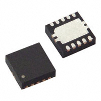
Small 3-mm × 3-mm SON-10 Package (DRC)
2 Applications
•
•
•
The inverter operates with a fixed-frequency pulse
width modulation (PWM) control topology. The device
has an internal current limit, overvoltage protection,
and a thermal shutdown for highest reliability under
fault conditions.
A switching frequency of typically 1.4 MHz allows the
use of small external components enabling a small
solution size.
Generic Negative Voltage Supply
Small-to-Medium Size OLED Displays
Bias Supply
The TPS63700 comes in a small 3-mm × 3-mm SON10 package.
Efficiency vs Output Current
90
VIN = 3.6 V
Device Information(1)
PART NUMBER
VIN = 5 V
TPS63700
80
VIN = 3.3 V
70
VIN = 4.2 V
PACKAGE
BODY SIZE (NOM)
VSON (10)
3.00 mm x 3.00 mm
(1) For all available packages, see the orderable addendum at
the end of the datasheet.
Efficiency %
60
50
40
30
20
10
0
0
100
200
300
400
IO − Output Current − mA
Typical Application Schematic
TPS63700
C2
VIN
R1
C1
0.1 μF
R2
VREF
0.22 μF
EN
FB
R3
OUT
PS_GND
D1
IN
VIN
2.7 V To 5.5 V
C4
10 μF
GND
VOUT
−5 V
SW
PowerPAD
COMP
L1
4.7 μH
C5
22 μF
C6
4.7 nF
1
An IMPORTANT NOTICE at the end of this data sheet addresses availability, warranty, changes, use in safety-critical applications,
intellectual property matters and other important disclaimers. PRODUCTION DATA.
�TPS63700
SLVS530D – SEPTEMBER 2005 – REVISED OCTOBER 2015
www.ti.com
Table of Contents
1
2
3
4
5
6
7
Features ..................................................................
Applications ...........................................................
Description .............................................................
Revision History.....................................................
Pin Configuration and Functions .........................
Specifications.........................................................
1
1
1
2
3
4
6.1
6.2
6.3
6.4
6.5
6.6
4
4
4
4
5
6
Absolute Maximum Ratings ......................................
ESD Ratings..............................................................
Recommended Operating Conditions.......................
Thermal Information ..................................................
Electrical Characteristics...........................................
Typical Characteristics ..............................................
Detailed Description .............................................. 7
7.1 Overview ................................................................... 7
7.2 Functional Block Diagram ......................................... 7
7.3 Feature Description................................................... 7
7.4 Device Functional Modes.......................................... 8
8
Application and Implementation .......................... 9
8.1 Application Information.............................................. 9
8.2 Typical Application .................................................... 9
8.3 System Example ..................................................... 15
9 Power Supply Recommendations...................... 16
10 Layout................................................................... 16
10.1 Layout Guidelines ................................................. 16
10.2 Layout Example .................................................... 16
11 Device and Documentation Support ................. 18
11.1
11.2
11.3
11.4
11.5
Device Support......................................................
Community Resources..........................................
Trademarks ...........................................................
Electrostatic Discharge Caution ............................
Glossary ................................................................
18
18
18
18
18
12 Mechanical, Packaging, and Orderable
Information ........................................................... 18
4 Revision History
NOTE: Page numbers for previous revisions may differ from page numbers in the current version.
Changes from Revision C (June 2013) to Revision D
•
Added Pin Configuration and Functions section, ESD Ratings table, Feature Description section, Device Functional
Modes, Application and Implementation section, Power Supply Recommendations section, Layout section, Device
and Documentation Support section, and Mechanical, Packaging, and Orderable Information section .............................. 1
Changes from Revision B (November 2007) to Revision C
•
2
Page
Page
Deleted Dissipation Ratings table and added Thermal Information table. ............................................................................. 4
Submit Documentation Feedback
Copyright © 2005–2015, Texas Instruments Incorporated
Product Folder Links: TPS63700
�TPS63700
www.ti.com
SLVS530D – SEPTEMBER 2005 – REVISED OCTOBER 2015
5 Pin Configuration and Functions
DRC Package
10-Pin VSON With PowerPAD™
Top View
COMP
1
10
GND
2
9
FB
VIN
3
8
OUT
EN
4
7
PS_GND
IN
5
6
SW
PowerPAD
VREF
Pin Functions
PIN
I/O
DESCRIPTION
NAME
NO.
COMP
1
I/O
Compensation pin for control, connect a 4.7 nF capacitor between this pin and GND
GND
2
—
Ground pin
VIN
3
I
Supply voltage input for control logic, connect a RC circuit of 10R and 100 nF to filter this supply voltage
EN
4
I
Enable pin (EN = GND: disabled; EN = VIN: enabled)
IN
5
I
Supply voltage for the power switch
SW
6
O
Inverter switch output
PS_GND
7
I
Connect to GND for control logic
OUT
8
I
Output voltage sense input
FB
9
I
Feedback pin for the voltage divider
VREF
10
O
Reference voltage output. Connect a 220-nF capacitor to ground. Connect the lower resistor of the negative
output voltage divider to this pin.
Submit Documentation Feedback
Copyright © 2005–2015, Texas Instruments Incorporated
Product Folder Links: TPS63700
3
�TPS63700
SLVS530D – SEPTEMBER 2005 – REVISED OCTOBER 2015
www.ti.com
6 Specifications
6.1 Absolute Maximum Ratings
over operating free-air temperature range unless otherwise noted (1)
MIN
MAX
UNIT
–0.3
6
V
VIN
V
–18
V
–0.3
VIN + 0.3
V
24
V
Operating virtual junction temperature, TJ
–40
150
°C
Storage temperature, Tstg
–65
150
°C
Input voltage at VIN (2)
Input voltage at IN
(2)
Minimum voltage at OUT
(2)
Voltage at EN, FB, COMP, PS_GND
(2)
Differential voltage between OUT to VIN
(1)
(2)
(2)
Stresses beyond those listed under Absolute Maximum Ratings may cause permanent damage to the device. These are stress ratings
only, and functional operation of the device at these or any other conditions beyond those indicated under Recommended Operating
Conditions is not implied. Exposure to absolute-maximum-rated conditions for extended periods may affect device reliability.
All voltage values are with respect to network ground terminal, unless otherwise noted.
6.2 ESD Ratings
VALUE
Human body model (HBM), per ANSI/ESDA/JEDEC JS-001, all pins
V(ESD)
(1)
(2)
Electrostatic discharge
(1)
UNIT
±2000
Charged device model (CDM), per JEDEC specification JESD22-C101,
all pins (2)
V
±1000
JEDEC document JEP155 states that 500-V HBM allows safe manufacturing with a standard ESD control process.
JEDEC document JEP157 states that 250-V CDM allows safe manufacturing with a standard ESD control process.
6.3 Recommended Operating Conditions
MIN
MAX
UNIT
Input voltage range, VIN
2.7
5.5
V
Operating free-air temperature, TA
–40
85
°C
Operating virtual junction temperature, TJ
–40
125
°C
6.4 Thermal Information
TPS63700
THERMAL METRIC
(1)
DRC (VSON)
UNIT
10 PINS
RθJA
Junction-to-ambient thermal resistance
41.2
°C/W
RθJC(top)
Junction-to-case(top) thermal resistance
62.8
°C/W
RθJB
Junction-to-board thermal resistance
16.6
°C/W
ψJT
Junction-to-top characterization parameter
1.2
°C/W
ψJB
Junction-to-board characterization parameter
16.8
°C/W
RθJC(bot)
Junction-to-case(bottom) thermal resistance
4.1
°C/W
(1)
4
For more information about traditional and new thermal metrics, see the Semiconductor and IC Package Thermal Metrics application
report, SPRA953.
Submit Documentation Feedback
Copyright © 2005–2015, Texas Instruments Incorporated
Product Folder Links: TPS63700
�TPS63700
www.ti.com
SLVS530D – SEPTEMBER 2005 – REVISED OCTOBER 2015
6.5 Electrical Characteristics
–40°C to 85°C, over recommended input voltage range, typical at an ambient temperature of 25°C (unless otherwise noted)
PARAMETER (1)
TEST CONDITIONS
MIN
TYP
MAX
UNIT
5.5
V
VIN = 3.6 V, IOUT = 0,
EN = VIN, no switching
VOUT = –5 V
330
400
μA
640
750
μA
EN = GND
0.2
1.5
μA
2.35
2.7
V
SUPPLY
VIN
Input voltage range
I(Q)
Quiescent
current
ISD
Shutdown supply current
UVLO
Undervoltage lockout
threshold
Pin VIN, IN
VIN
IN
2.7
2.1
Thermal shutdown temperature
TSD
Junction temperature
decreasing
Thermal Shutdown hysteresis
150
°C
5
°C
CONTROL STAGE
VEN
High level input voltage
VEN
Low level input voltage
IEN
Input current
1.4
EN = VIN or GND
V
0.4
V
0.01
0.1
μA
mA
POWER SWITCH
ILIM
Inverter switch current limit
2.7 V < VIN < 5.5 V
1000
1140
VIN = 3.6 V
860
440
600
VIN = 5 V
370
500
RDS(ON)
Inverter switch on-resistance
DMAX
Maximum duty cycle
inverting converter
87.5%
DMIN
Minimum duty cycle
inverting converter
12.5%
fS
Oscillator frequency
1250
1380
1500
mΩ
kHz
OUTPUT
VOUT
Adjustable output
voltage range
VOUT
DC output accuracy
PWM mode, device switching
VREF
Reference voltage
IREF = 10 μA
VOVP
Output overvoltage
protection
VFB
Negative feedback
regulation voltage
VIN = 2.7 V to 5.5 V
IFB
Negative feedback input bias current
VFBN = 0.1 VREF
(1)
–15
–2
V
1.225
V
±3%
1.2
1.213
–19
–0.024
0
V
0.024
2
V
nA
Parameter does not include tolerance of external resistors.
Submit Documentation Feedback
Copyright © 2005–2015, Texas Instruments Incorporated
Product Folder Links: TPS63700
5
�TPS63700
SLVS530D – SEPTEMBER 2005 – REVISED OCTOBER 2015
www.ti.com
6.6 Typical Characteristics
400
Maximum Output Current − mA
350
VO = −5 V
300
250
VO = −12 V
200
VO = −15 V
150
100
50
0
2.5
3
3.5
4
4.5
5
5.5
VI − Input Voltage − V
Figure 1. Maximum Output Current vs Input Voltage
6
Submit Documentation Feedback
Copyright © 2005–2015, Texas Instruments Incorporated
Product Folder Links: TPS63700
�TPS63700
www.ti.com
SLVS530D – SEPTEMBER 2005 – REVISED OCTOBER 2015
7 Detailed Description
7.1 Overview
The TPS63700 is a DC/DC converter for negative output voltages using buck-boost topology. It operates with an
input voltage range of 2.7 V to 5.5 V and generates a negative output voltage down to –15 V. The output is
controlled by a fixed-frequency, pulse-width-modulated (PWM) regulator. In normal operation mode, the
converter operates at continuous conduction mode (CCM). At light loads it can enter discontinuous conduction
mode (DCM).
7.2 Functional Block Diagram
VIN
VIN
VIN
Temperature
GND
Oscillator
Control
VIN
PS_GND
OUT
Control Logic
EN
−
COMP
FB
+
VREF
Gate
IN
Control
+
−
SW
IN
7.3 Feature Description
7.3.1 Enable
Applying GND signal at the EN pin disables the converter, where all internal circuitry is turned off. The device
now just consumes low shutdown current flowing into the VIN pin. The output load of the converter is also
disconnected from the battery as described in Load Disconnect. Pulling the EN pin to VIN enables the converter.
Internal circuitry, necessary to operate the converter, is then turned on.
7.3.2 Load Disconnect
The device supports complete load disconnection when the converter is disabled. The converter turns off the
internal PMOS switch, thus no DC current path remains between load and input voltage source.
7.3.3 Output Overvoltage Protection
The converter has an output overvoltage protection implemented. The output voltage is limited to –19 V in case
the feedback connection from the output to the FB pin is open.
Submit Documentation Feedback
Copyright © 2005–2015, Texas Instruments Incorporated
Product Folder Links: TPS63700
7
�TPS63700
SLVS530D – SEPTEMBER 2005 – REVISED OCTOBER 2015
www.ti.com
Feature Description (continued)
7.3.4 Undervoltage Lockout
An undervoltage lockout prevents the device from starting up and operating if the supply voltage at VIN is lower
than the programmed threshold shown in the Electrical Characteristics table. The device automatically shuts
down the converter when the supply voltage at VIN falls below this threshold. Nevertheless, parts of the control
circuits remain active, which is different than device shutdown using EN inputs. The undervoltage lockout
function is implemented to prevent device malfunction.
7.3.5 Overtemperature Shutdown
The device automatically shuts down if the implemented internal temperature detector detects a chip temperature
above the programmed threshold shown in the electrical characteristics table. It starts operating again when the
chip temperature decreases. A built-in temperature hysteresis avoids undefined operation caused by ringing from
over-temperature shutdown.
7.4 Device Functional Modes
7.4.1 Soft-Start
The converter has a soft-start function. When the converter is enabled, the implemented switch current limit
ramps up slowly to its nominal value. Soft-start is implemented to limit the input current during start-up to avoid
high peak currents at the battery which could interfere with other systems connected to the same battery.
Without soft-start, uncontrolled input peak currents flow to charge up the output capacitors and to supply the load
during start-up. This would cause significant voltage drops across the series resistance of the battery and its
connections.
7.4.2 PWM Operation
The converter operates in a fixed-frequency, pulse-width-modulated control scheme. The on-time of the switches
varies depending on input-to-output voltage ratio and the load. During this on-time, the inductor connected to the
converter is charged with current. In the remaining time, the time period set by the fixed operating frequency, the
inductor discharges into the output capacitor via the rectifier diode. At medium to heavy loads the inductor
current is continuous and the device operates in continuous conduction mode (CCM).
7.4.3 Power Save Mode Operation
As the load current decreases, the converter enters Power Save Mode. Entering Power Save Mode happens at
the boundary to discontinuous conduction mode (DCM). During light load, the inductor current of this converter
can become discontinuous. In this case, the control circuit of the controller output automatically takes care of
these changing conditions to always operate with an optimum control setup.
7.4.4 Control
The controller circuit of the converter is based on a fixed-frequency, multiple-feed-forward controller topology.
Input voltage, output voltage, and voltage drop across the switch are monitored and forwarded to the regulator.
Changes in the operating conditions of the converter directly affect the duty cycle.
The error amplifier compares the voltage at FB pin with GND to generate an accurate and stable output voltage.
The error amplifier is internally compensated. At light loads, the converter operates in discontinuous conduction
mode (DCM).
If the load will be further decreased, the energy transmitted to the output capacitor cannot be absorbed by the
load and would lead to an increase of the output voltage. In this case, the converter limits the output voltage
increase by skipping switch pulses.
8
Submit Documentation Feedback
Copyright © 2005–2015, Texas Instruments Incorporated
Product Folder Links: TPS63700
�TPS63700
www.ti.com
SLVS530D – SEPTEMBER 2005 – REVISED OCTOBER 2015
8 Application and Implementation
NOTE
Information in the following applications sections is not part of the TI component
specification, and TI does not warrant its accuracy or completeness. TI’s customers are
responsible for determining suitability of components for their purposes. Customers should
validate and test their design implementation to confirm system functionality.
8.1 Application Information
The TPS63700 DC/DC converter is intended for systems typically powered by a single-cell Li-ion or Li-polymer
battery with a terminal voltage between 2.7 V up to 4.2 V. Due to the recommended input voltage going up to 5.5
V, the device is also suitable for 3-cell alkaline, NiCd,or NiMH batteries, as well as regulated supply voltages of
3.3 V or 5 V.
8.2 Typical Application
TPS63700
R2
150 kW
C2
VIN
VREF
EN
FB
0.22 mF
10 W
C1
0.1 mF
VIN
D1
SW
IN
C4
10 mF
10pF
R3
619 kW
OUT
PS_GND
2.7 V To 5.5 V
C3
R4
100 kW
VOUT, –5V
SL02
GND
PowerPAD
COMP
C5
4x4.7 mF
L1
4.7 mH
C6
4.7 nF
Figure 2. Circuit for –5-V Output
8.2.1 Design Requirements
The design of the inverter can be adapted to different output voltage and load current needs by choosing
external components appropriately. The following design procedure is adequate for the whole VIN, VOUT and load
current range of TPS63700.
Table 1 shows the list of components for the Application Curves.
Table 1. List of Components
REFERENCE
C1, C2, C3, C4,
DESCRIPTION
X7R/X5R ceramic
C5
4 × 4.7 μF X7R/X5R ceramic
D1
SL03/SL02 Vishay
L1
–5V: TDK VLF4012 4R7, TDK SLF60254R7, Coilcraft LPS4018-472,
–12V: Sumida CDRH5D18 10 μH
Submit Documentation Feedback
Copyright © 2005–2015, Texas Instruments Incorporated
Product Folder Links: TPS63700
9
�TPS63700
SLVS530D – SEPTEMBER 2005 – REVISED OCTOBER 2015
www.ti.com
8.2.2 Detailed Design Procedure
8.2.2.1 Programming the Output Voltage: Converter
The output voltage of the TPS63700 converter can be adjusted with an external resistor divider connected to the
FB pin. The reference point of the feedback divider is the reference voltage VREF with 1.213 V. The typical value
of the voltage at the FB pin is 0 V. The minimum recommended output voltage at the converter is –15 V. The
feedback divider current should be 10 μA. The voltage across R2 is 1.213 V. Based on those values, the
recommended value for R2 should be 120 kΩ to 200 kΩ in order to set the divider current at the required value.
The value of the resistor R3 can then be calculated using Equation 1, depending on the needed output voltage
(VOUT).
æV
ö
- VOUT
R3 = R2 ´ ç REF
- 1÷
V
REF
è
ø
(1)
For example, if an output voltage of –5 V is needed and a resistor of 150 kΩ has been chosen for R2, a 619-kΩ
resistor is needed to program the desired output voltage.
8.2.2.1.1 Inductor Selection
An inductive converter normally requires two main passive components for storing energy during the conversion.
An inductor and a storage capacitor at the output are required.
The average inductor current depends on the output load, the input voltage VIN, and the output voltage VOUT. It
can be estimated with Equation 2, which shows the formula for the inverting converter.
V - VOUT
ILavg = IN
´ IOUT
VIN ´ 0.8
where
•
ILavg= Average inductor current
(2)
An important parameter for choosing the inductor is the desired current ripple in the inductor.
A ripple current value between 20% and 80% of the average inductor current can be considered as reasonable,
depending on the application requirements. A smaller ripple reduces the losses in the inductor, as well as output
voltage ripple and EMI. But in the same way, the inductor becomes larger and more expensive.
Keeping those parameters in mind, the possible inductor value can be calculated using Equation 3.
VIN ´ VOUT
L=
DIL ´ (VOUT - VIN )´ f
where
•
•
•
ΔIL = Peak-to-peak ripple current
f = Switching frequency
L = Inductor value
(3)
With the known inductor current ripple, the peak inductor value can be approximated with Equation 4. The peak
current through the switch and the inductor depends also on the output load, the input voltage VIN, and the output
voltage VOUT. To select the right inductor, it is recommended to keep the possible peak inductor current below
the current-limit threshold of the power switch. For example, the current-limit threshold of the TPS63700 switch
for the inverting converter is nominally 1000 mA.
V - VOUT
DI
IL max = IN
´ IOUT + L
VIN ´ 0.8
2
where
•
•
ILMAX = Peak inductor current
ΔIL = Peak-to-peak ripple current
(4)
With Equation 5, the inductor current ripple at a given inductor can be approximated.
10
Submit Documentation Feedback
Copyright © 2005–2015, Texas Instruments Incorporated
Product Folder Links: TPS63700
�TPS63700
www.ti.com
SLVS530D – SEPTEMBER 2005 – REVISED OCTOBER 2015
DIL =
VIN ´ VOUT
L ´ (VOUT - VIN )´ f
where
•
•
•
ΔIL = Peak-to-peak ripple current
L = Inductor value
f = Switching frequency
(5)
Care has to be taken for the possibility that load transients and losses in the circuit can lead to higher currents as
estimated in Equation 4. Also, the losses caused by magnetic hysteresis losses and copper losses are a major
parameter for total circuit efficiency.
The following inductor series from different suppliers have been tested with the TPS63700 converter, see
Table 2.
Table 2. List of Inductors
Output Voltage
Vendor
SUGGESTED INDUCTOR
VLF4012 4.7 μH
–5 V
TDK
–5 V
Coilcraft
–12 V
Sumida
CDRH5D18 10 μH
–12 V
Coilcraft
MOS6020 10 μH
SLF6025-4.7 μH
LPS4018 4.7 μH
LPS3015 4.7 μH
8.2.2.2 Capacitor Selection
8.2.2.2.1 Input Capacitor
At least a 10-μF ceramic input capacitor is recommended for a good transient behavior of the regulator, and EMI
behavior of the total power supply circuit.
8.2.2.2.2 Output Capacitors
One of the major parameters necessary to define the capacitance value of the output capacitor is the maximum
allowed output voltage ripple of the converter. This ripple is determined by two parameters of the capacitor, the
capacitance and the ESR. It is possible to calculate the minimum capacitance needed for the defined ripple,
supposing that the ESR is zero, by using Equation 6 for the inverting converter output capacitor.
IOUT ´ VOUT
Cmin =
fS ´ DV ´ (VOUT - VIN )
where
•
•
•
f = Switching frequency
ΔV = Maximum allowed ripple
Cmin = Minimum capacitance
(6)
With a chosen ripple voltage in the range of 10 mV, a minimum capacitance of 12 μF is needed. The total ripple
is larger due to the ESR of the output capacitor. This additional component of the ripple can be calculated using
Equation 7 .
DVESR = IOUT ´ RESR
where
•
•
ΔVESR = Voltage ripple caused by RESR of capacitor
RESR = Equivalent series resistance of capacitor
(7)
Submit Documentation Feedback
Copyright © 2005–2015, Texas Instruments Incorporated
Product Folder Links: TPS63700
11
�TPS63700
SLVS530D – SEPTEMBER 2005 – REVISED OCTOBER 2015
www.ti.com
An additional ripple of 2 mV is the result of using a typical ceramic capacitor with an ESR in a 10-mΩ range. The
total ripple is the sum of the ripple caused by the capacitance, and the ripple caused by the ESR of the capacitor.
In this example, the total ripple is 12 mV. Additional ripple is caused by load transients. When the load current
increases rapidly, the output capacitor must provide the additional current until the inductor current has been
increased by the control loop by setting a higher on-time at the main switch (duty cycle). The higher duty cycle
results in longer inductor charging periods, but the rate of increase of the inductor current is also limited by the
inductance itself. When the load current decreases rapidly, the output capacitor needs to store the excessive
energy (stored in the inductor) until the regulator has decreased the inductor current by reducing the duty cycle.
The recommendation is to use higher capacitance values, as the previous calculations show.
8.2.2.3 Stabilizing the Control Loop
8.2.2.3.1 Feedback Divider
To speed up the control loop, a feed-forward capacitor of 10 pF is recommended in the feedback divider, parallel
to R3.
To avoid coupling noise into the control loop from the feed-forward capacitor, the feed-forward effect can be
bandwidth-limited by adding series resistor R4. A value in the range of 100 kΩ is suitable. The higher the
resistance, the lower the noise coupled into the control loop system.
8.2.2.3.2 Compensation Capacitor
The control loop of the converter is completely compensated internally. However the internal feed-forward system
requires an external capacitor. A 4.7-nF capacitor at the COMP pin of the converter is recommended.
12
Submit Documentation Feedback
Copyright © 2005–2015, Texas Instruments Incorporated
Product Folder Links: TPS63700
�TPS63700
www.ti.com
SLVS530D – SEPTEMBER 2005 – REVISED OCTOBER 2015
8.2.3 Application Curves
90
VIN = 3.6 V
90
VIN = 5 V
80
80
VIN = 4.2 V
VIN = 3.3 V
70
50
40
30
VIN = 3.3 V
50
40
30
20
20
10
10
100
0
200
300
0
400
0
100
50
IO − Output Current − mA
90
200
90
VIN = 5 V
IOUT = 200 mA
IOUT = 50 mA
80
70
VIN = 3.3 V
250
Figure 4. Efficiency vs Output Current,
VOUT –12 V
80
VIN = 4.2 V
IOUT = 20 mA
70
60
Efficiency %
60
50
40
50
40
30
30
20
20
10
10
0
150
IO − Output Current − mA
Figure 3. Efficiency vs Output Current,
VOUT –5 V
Efficiency %
VIN = 3.6 V
60
Efficiency %
Efficiency %
VIN = 4.2 V
70
60
0
VIN = 5 V
0
20
40
0
2.5
60 80 100 120 140 160 180 200
IO − Output Current − mA
4
4.5
5
5.5
VIN − Input Voltage − V
Figure 5. Efficiency vs Output Current,
VOUT –15 V
90
3.5
3
Figure 6. Efficiency vs Input Voltage,
VOUT –5 V
−5.1
IOUT = 150 mA
IOUT = 50 mA
80
IOUT = 20 mA
VOUT− Output Voltage − V
70
Efficiency %
60
50
40
30
20
VIN = 5 V
−5.05
−5
VIN = 3.6 V
VIN = 3.3 V
−4.95
10
0
2.5
3
3.5
4.5
4
VIN − Input Voltage − V
5.5
5
−4.9
0
50
100
150
200
250
300
350
400
IOUT − Output Current − mA
Figure 7. Efficiency vs Input Voltage,
VOUT –12 V
Figure 8. Output Voltage vs Output Current
Submit Documentation Feedback
Copyright © 2005–2015, Texas Instruments Incorporated
Product Folder Links: TPS63700
13
�TPS63700
SLVS530D – SEPTEMBER 2005 – REVISED OCTOBER 2015
www.ti.com
−12.4
VIN = 3.6 V,
ILOAD = 20 mA
VOUT− Output Voltage − V
−12.3
VOUT 20 mV/div, AC
−12.2
VIN = 5 V
−12.1
VIN = 3.6 V
−12
VIN = 3.3 V
−11.9
−11.8
ICOIL 200 mA/div, DC
VOUT = –5 V
−11.7
0
50
100
150
200
250
IOUT − Output Current − mA
t - Time - 500 ns/div
Figure 9. Output Voltage vs Output Current
VIN = 3.6 V,
ILOAD = 95 mA
VOUT 20 mV/div, AC
Figure 10. Output Voltage in
Discontinuous Conduction Mode
VIN = 3.6V,
I
= 45mA to 150mA
LOAD
V
OUT
100mV/div, AC
ICOIL 200 mA/div, DC
VOUT = –5 V
V OUT = –5V
t - Time - 500 ns/div
LOAD
50mA/div, DC
t-Time-2ms/div
Figure 12. Load Transient Response,
–5 V, 45 to 150 mA
Figure 11. Output Voltage in
Continuous Conduction Mode
VIN = 3.6 V to 4.2 V,
ILOAD = 100 mA,
VOUT = –5 V
4.2 V
I
EN 2 V/div, DC
VIN 500 mV/div, DC
VIN = 3.6 V,
Load = 22 W,
VOUT = –5 V
3.6 V
ICOIL 200 mA/div, DC
VOUT 100 mV/div, DC
VOUT 2 V/div, DC
t - Time - 500 ms/div
t - Time - 2 ms/div
Figure 13. Line Transient Response, –5 V
14
Submit Documentation Feedback
Figure 14. Start-Up After Enable, –5 V
Copyright © 2005–2015, Texas Instruments Incorporated
Product Folder Links: TPS63700
�TPS63700
www.ti.com
SLVS530D – SEPTEMBER 2005 – REVISED OCTOBER 2015
8.3 System Example
TPS63700
C2
10 W
C1
0.1 mF
VIN
VREF
EN
FB
0.22 mF
OUT
PS_GND
VIN
2.7 V To 5.5 V
C4
10 mF
D1
SW
IN
GND
PowerPAD
COMP
SL03
L1
10 mH
R2
121 kW
C3
10pF
R3
1.2 MW
R4
100 kW
VOUT, –12V
C5
4x4.7 mF
C6
4.7 nF
Figure 15. Circuit for –12-V Output
Submit Documentation Feedback
Copyright © 2005–2015, Texas Instruments Incorporated
Product Folder Links: TPS63700
15
�TPS63700
SLVS530D – SEPTEMBER 2005 – REVISED OCTOBER 2015
www.ti.com
9 Power Supply Recommendations
The power supply to the TPS63700 needs to have a current rating according to the input supply voltage, output
voltage and output current of the TPS63700.
10 Layout
10.1 Layout Guidelines
For all switching power supplies the layout is an important step in the design, especially at high peak currents
and high switching frequencies. If the layout is not carefully done, the regulator could show stability problems as
well as EMI problems. Therefore, use wide and short traces for the main current paths, and for the power-ground
tracks. The input and output capacitors should be placed as close as possible to the IC. The diode need to be
connected closest to the SW pin to minimize parasitic inductance. For low noise operation small bypass
capacitors CIN BP and COUT BP in the nF range can be added close to the IC.
The feedback divider should be placed as close as possible to the VREF pin of the IC. Use short traces when
laying out the control ground. Figure 18 shows the layout of the EVM board.
10.2 Layout Example
Figure 16. Layout Considerations, Top View
16
Submit Documentation Feedback
Copyright © 2005–2015, Texas Instruments Incorporated
Product Folder Links: TPS63700
�TPS63700
www.ti.com
SLVS530D – SEPTEMBER 2005 – REVISED OCTOBER 2015
Layout Example (continued)
VOUT sense
Figure 17. Layout Considerations, Bottom View
TPS63700
10 W
C4
0.1 mF
VIN
2.7V to 5.5V
VIN
VREF
EN
FB
OUT
PS_GND
10 mF
CIN BP
22 nF
D1
SL03
GND
R2
121 kW
C6
10 pF
R2
1.2 MW
SW
IN
C1
C5
0.22 mF
PowerPAD
COMP
L1
10 mH
COUT BP
10 nF
R4
100 kW
VOUT, -12 V
C8,C9,C10,C11
4x4.7 mF
C6
4.7 nF
Figure 18. Layout Circuit
Submit Documentation Feedback
Copyright © 2005–2015, Texas Instruments Incorporated
Product Folder Links: TPS63700
17
�TPS63700
SLVS530D – SEPTEMBER 2005 – REVISED OCTOBER 2015
www.ti.com
11 Device and Documentation Support
11.1 Device Support
11.1.1 Third-Party Products Disclaimer
TI'S PUBLICATION OF INFORMATION REGARDING THIRD-PARTY PRODUCTS OR SERVICES DOES NOT
CONSTITUTE AN ENDORSEMENT REGARDING THE SUITABILITY OF SUCH PRODUCTS OR SERVICES
OR A WARRANTY, REPRESENTATION OR ENDORSEMENT OF SUCH PRODUCTS OR SERVICES, EITHER
ALONE OR IN COMBINATION WITH ANY TI PRODUCT OR SERVICE.
11.2 Community Resources
The following links connect to TI community resources. Linked contents are provided "AS IS" by the respective
contributors. They do not constitute TI specifications and do not necessarily reflect TI's views; see TI's Terms of
Use.
TI E2E™ Online Community TI's Engineer-to-Engineer (E2E) Community. Created to foster collaboration
among engineers. At e2e.ti.com, you can ask questions, share knowledge, explore ideas and help
solve problems with fellow engineers.
Design Support TI's Design Support Quickly find helpful E2E forums along with design support tools and
contact information for technical support.
11.3 Trademarks
PowerPAD, E2E are trademarks of Texas Instruments.
All other trademarks are the property of their respective owners.
11.4 Electrostatic Discharge Caution
These devices have limited built-in ESD protection. The leads should be shorted together or the device placed in conductive foam
during storage or handling to prevent electrostatic damage to the MOS gates.
11.5 Glossary
SLYZ022 — TI Glossary.
This glossary lists and explains terms, acronyms, and definitions.
12 Mechanical, Packaging, and Orderable Information
The following pages include mechanical, packaging, and orderable information. This information is the most
current data available for the designated devices. This data is subject to change without notice and revision of
this document. For browser-based versions of this data sheet, refer to the left-hand navigation.
18
Submit Documentation Feedback
Copyright © 2005–2015, Texas Instruments Incorporated
Product Folder Links: TPS63700
�PACKAGE OPTION ADDENDUM
www.ti.com
14-Oct-2022
PACKAGING INFORMATION
Orderable Device
Status
(1)
Package Type Package Pins Package
Drawing
Qty
Eco Plan
(2)
Lead finish/
Ball material
MSL Peak Temp
Op Temp (°C)
Device Marking
(3)
Samples
(4/5)
(6)
TPS63700DRCR
ACTIVE
VSON
DRC
10
3000
RoHS & Green
NIPDAU
Level-2-260C-1 YEAR
-40 to 85
NUB
Samples
TPS63700DRCT
ACTIVE
VSON
DRC
10
250
RoHS & Green
NIPDAU
Level-2-260C-1 YEAR
-40 to 85
NUB
Samples
TPS63700DRCTG4
ACTIVE
VSON
DRC
10
250
RoHS & Green
NIPDAU
Level-2-260C-1 YEAR
-40 to 85
NUB
Samples
(1)
The marketing status values are defined as follows:
ACTIVE: Product device recommended for new designs.
LIFEBUY: TI has announced that the device will be discontinued, and a lifetime-buy period is in effect.
NRND: Not recommended for new designs. Device is in production to support existing customers, but TI does not recommend using this part in a new design.
PREVIEW: Device has been announced but is not in production. Samples may or may not be available.
OBSOLETE: TI has discontinued the production of the device.
(2)
RoHS: TI defines "RoHS" to mean semiconductor products that are compliant with the current EU RoHS requirements for all 10 RoHS substances, including the requirement that RoHS substance
do not exceed 0.1% by weight in homogeneous materials. Where designed to be soldered at high temperatures, "RoHS" products are suitable for use in specified lead-free processes. TI may
reference these types of products as "Pb-Free".
RoHS Exempt: TI defines "RoHS Exempt" to mean products that contain lead but are compliant with EU RoHS pursuant to a specific EU RoHS exemption.
Green: TI defines "Green" to mean the content of Chlorine (Cl) and Bromine (Br) based flame retardants meet JS709B low halogen requirements of