Product
Folder
Order
Now
Support &
Community
Tools &
Software
Technical
Documents
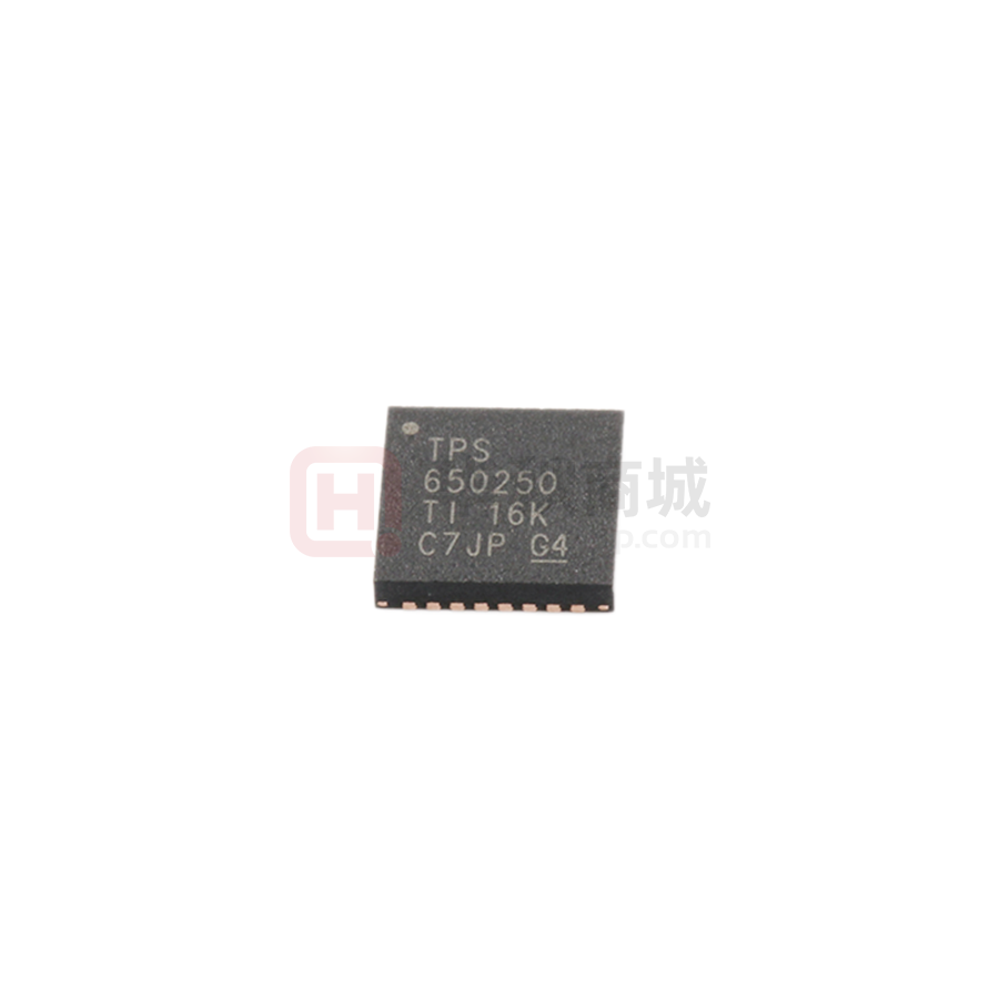
TPS650250
SLVS843B – DECEMBER 2008 – REVISED MAY 2018
TPS650250 Power Management IC (PMIC) for SoCs and Multirail Subsystems
1 Features
•
1
•
•
•
•
•
•
•
•
•
•
•
1.6 A, 97% Efficient Step-Down Converter for
System Voltage (VDCDC1)
– 3.3 V, 2.8 V, or Adjustable
0.8 A, up to 95% Efficient Step-Down Converter
for Memory Voltage (VDCDC2)
– 1.8 V, 2.5 V, or Adjustable
0.8 A, 90% Efficient Step-Down Converter for
Processor Core (VDCDC3)
Adjustable Output Voltage on VDCDC3
30-mA LDO for Vdd_alive
2 × 200 mA General-Purpose LDOs (LDO1 and
LDO2)
Dynamic Voltage Management for Processor Core
LDO1 and LDO2 Voltage Externally Adjustable
Separate Enable Pins for Inductive Converters
2.25-MHz Switching Frequency
85-μA Quiescent Current
Thermal Shutdown Protection
Device Information(1)
PART NUMBER
PACKAGE
TPS650250
VQFN (32)
(1) For all available packages, see the orderable addendum at
the end of the datasheet.
Detailed Block Diagram
TPS650250
1R
VCC
Vbat
1 mF
VINDCDC1
Vbat
10 mF
STEP-DOWN
CONVERTER
1600 mA
EN_DCDC1
ENABLE
VINDCDC2
Vbat
DCDC2
(memory )
10 mF
STEP-DOWN
CONVERTER
800 mA
EN_DCDC2
ENABLE
VINDCDC3
10 mF
DCDC3 (core)
ENABLE
STEP-DOWN
CONVERTER
800 mA
2 Applications
Cellular, Smart Phones
GPS
Digital Still Cameras
Split Supply DSP and μP Solutions
Samsung ARM-Based Processors
EN_DCDC3
The TPS650250 device integrates two generalpurpose 200-mA LDO voltage regulators. Both LDOs
operate with an input voltage range from 1.5 V to 6.5
V, allowing them to be supplied from one of the stepdown converters. The output voltage of all rails can
be set with an external resistor divider and enabled
with an input pin. Additionally, a 30-mA LDO is
typically used to provide power to an always-on rail.
2.2 mH
VDCDC1
R1
22 mF
DEFDCDC1
PGND1
R2
2.5 V / 1.8 V
or adjustable
L2
2.2 mH
VDCDC2
R3
22 mF
DEFDCDC2
PGND2
R4
L3
2.2 mH
VDCDC3
R5
22 mF
DEFDCDC3
PGND3
R6
MODE
PWM/ PFM
VIN_LDO
VIN
VLDO1
200 mA LDO
EN_LDO
ENABLE
VLDO1
FB_LDO1 R7
2.2 mF
R8
3 Description
The TPS650250 device is an integrated power
management IC for applications requiring multiple
power rails. The TPS650250 provides three highly
efficient, step-down converters targeted at providing
the core voltage, peripheral, I/O and memory rails in
a processor-based system. All three step-down
converters, controlled by the MODE pin, enter a lowpower mode at light load for maximum efficiency or
operate in forced fixed frequency PWM mode.
3.3 V / 2.8 V
or adjustable
L1
DCDC1 (I/O)
Vbat
•
•
•
•
•
BODY SIZE (NOM)
5.00 mm × 5.00 mm
VLDO2
200 mA LDO
VLDO2
FB_LDO2 R9
R10
EN_Vdd_alive
ENABLE
VLDO3
Vdd_alive
VCC
Vbat
2.2 mF
1V
2.2 mF
30 mA LDO
R11
I/O voltage
PWRFAIL _SNS
R12
-
PWRFAIL
R19
+
Vref = 1 V
AGND1
AGND2
1
An IMPORTANT NOTICE at the end of this data sheet addresses availability, warranty, changes, use in safety-critical applications,
intellectual property matters and other important disclaimers. PRODUCTION DATA.
�TPS650250
SLVS843B – DECEMBER 2008 – REVISED MAY 2018
www.ti.com
Table of Contents
1
2
3
4
5
6
Features ..................................................................
Applications ...........................................................
Description .............................................................
Revision History.....................................................
Pin Configuration and Functions .........................
Specifications.........................................................
6.1
6.2
6.3
6.4
6.5
6.6
6.7
6.8
6.9
6.10
7
1
1
1
2
3
4
Absolute Maximum Ratings ...................................... 4
ESD Ratings.............................................................. 4
Recommended Operating Conditions....................... 5
Thermal Information .................................................. 5
Dissipation Ratings ................................................... 6
Electrical Characteristics........................................... 6
Electrical Characteristics VDCDC1........................... 8
Electrical Characteristics VDCDC2........................... 8
Electrical Characteristics VDCDC3........................... 9
Typical Characteristics .......................................... 10
Detailed Description ............................................ 12
7.1 Overview ................................................................. 12
7.2 Functional Block Diagram ....................................... 12
7.3 Feature Description................................................. 13
7.4 Device Functional Modes........................................ 15
8
Application and Implementation ........................ 16
8.1 Application Information............................................ 16
8.2 Typical Application ................................................. 17
9 Power Supply Recommendations...................... 24
10 Layout................................................................... 24
10.1 Layout Guidelines ................................................. 24
10.2 Layout Example .................................................... 25
11 Device and Documentation Support ................. 26
11.1
11.2
11.3
11.4
11.5
11.6
11.7
Device Support......................................................
Documentation Support ........................................
Receiving Notification of Documentation Updates
Community Resources..........................................
Trademarks ...........................................................
Electrostatic Discharge Caution ............................
Glossary ................................................................
26
26
26
26
26
27
27
12 Mechanical, Packaging, and Orderable
Information ........................................................... 27
4 Revision History
NOTE: Page numbers for previous revisions may differ from page numbers in the current version.
Changes from Revision A (September 2014) to Revision B
Page
•
Changed the title of the data sheet ....................................................................................................................................... 1
•
Changed the Handling Ratings table to ESD Ratings and moved the storage temperature to the Absolute Maximum
Ratings table........................................................................................................................................................................... 4
•
Added the Development Support, Documentation Support, Receiving Notification of Documentation Updates, and
Community Resources sections ........................................................................................................................................... 26
•
Changed the Electrostatic Discharge Caution statement..................................................................................................... 26
Changes from Original (December 2008) to Revision A
•
2
Page
Added Handling Rating table, Feature Description section, Device Functional Modes, Application and
Implementation section, Power Supply Recommendations section, Layout section, Device and Documentation
Support section, and Mechanical, Packaging, and Orderable Information section................................................................ 1
Submit Documentation Feedback
Copyright © 2008–2018, Texas Instruments Incorporated
Product Folder Links: TPS650250
�TPS650250
www.ti.com
SLVS843B – DECEMBER 2008 – REVISED MAY 2018
5 Pin Configuration and Functions
DEFDCDC3
AGND1
PWRFAIL_SNS
Vcc
VINDCDC2
L2
PGND2
VDCDC2
RHB Package
32-Pin VQFN With Exposed Thermal Pad
Top View
32 31 30 29 28 27 26 25
VDCDC3
PGND3
L3
VINDCDC3
VINDCDC1
L1
PGND1
VDCDC1
1
2
3
4
5
6
7
8
24
23
22
21
20
19
18
17
TPS650250
EN_Vdd_alive
MODE
DEFDCDC2
PWRFAIL
EN_DCDC1
EN_DCDC2
EN_DCDC3
EN_LDO
DEFDCDC1
FB_LDO2
FB_LDO1
Vdd_alive
AGND2
VLDO2
VINLDO
VLDO1
9 10 11 12 13 14 15 16
Pin Functions
PIN
NAME
NO.
I/O
DESCRIPTION
SWITCHING REGULATOR SECTION
AGND1
31
—
Analog ground connection. All analog ground pins are connected internally on the chip.
AGND2
13
—
Analog ground connection. All analog ground pins are connected internally on the chip.
Thermal pad
—
—
Connect the power pad to analog ground.
VINDCDC1
5
L1
6
—
VDCDC1
8
I
PGND1
7
—
I
I
VINDCDC2
28
L2
27
—
VDCDC2
25
I
PGND2
26
—
VINDCDC3
4
L3
3
—
VDCDC3
1
I
PGND3
2
—
Vcc
29
I
DEFDCDC1
9
I
I
Input voltage for VDCDC1 step-down converter. This must be connected to the same voltage supply as
VINDCDC2, VINDCDC3 and VCC.
Switch pin of VDCDC1 converter. The VDCDC1 inductor is connected here.
VDCDC1 feedback voltage sense input, connect directly to VDCDC1.
Power ground for VDCDC1 converter.
Input voltage for VDCDC2 step-down converter. This must be connected to the same voltage supply as
VINDCDC1, VINDCDC3 and VCC.
Switch pin of VDCDC2 converter. The VDCDC2 inductor is connected here.
VDCDC2 feedback voltage sense input, connect directly to VDCDC2.
Power ground for VDCDC2 converter.
Input voltage for VDCDC3 step-down converter. This must be connected to the same voltage supply as
VINDCDC1, VINDCDC2 and VCC.
Switch pin of VDCDC3 converter. The VDCDC3 inductor is connected here.
VDCDC3 feedback voltage sense input, connect directly to VDCDC3.
Power ground for VDCDC3 converter.
Power supply for digital and analog circuitry of DCDC1, DCDC2 and DCDC3 DC-DC converters. This must be
connected to the same voltage supply as VINDCDC3, VINDCDC1 and VINDCDC2.
Input signal indicating default VDCDC1 voltage, 0 = 2.8V, 1 = 3.3V .
This pin can also be connected to a resistor divider between VDCDC1 and GND. In this case the output
voltage of the DCDC1 converter can be set in a range from 0.6V to VINDCDC1.
Submit Documentation Feedback
Copyright © 2008–2018, Texas Instruments Incorporated
Product Folder Links: TPS650250
3
�TPS650250
SLVS843B – DECEMBER 2008 – REVISED MAY 2018
www.ti.com
Pin Functions (continued)
PIN
NAME
NO.
I/O
DESCRIPTION
Input signal indicating default VDCDC2 voltage, 0 = 1.8V, 1 = 2.5V .
DEFDCDC2
22
I
This pin can also be connected to a resistor divider between VDCDC2 and GND. In this case the output
voltage of the DCDC2 converter can be set in a range from 0.6V to VINDCDC2.
DEFDCDC3
32
I
This pin must be connected to a resistor divider between VDCDC3 and GND. The output voltage of the
DCDC3 converter can be set in a range from 0.6V to VINDCDC3.
EN_DCDC1
EN_DCDC2
20
I
VDCDC1 enable pin. A logic high enables the regulator, a logic low disables the regulator.
19
I
VDCDC2 enable pin. A logic high enables the regulator, a logic low disables the regulator.
EN_DCDC3
18
I
VDCDC3 enable pin. A logic high enables the regulator, a logic low disables the regulator.
LDO REGULATOR SECTION
VINLDO
15
I
Input voltage for LDO1 and LDO2.
VLDO1
16
O
Output voltage of LDO1.
VLDO2
14
O
Output voltage of LDO2.
EN_LDO
17
I
Enable input for LDO1 and LDO2. Logic high enables the LDOs, logic low disables the LDOs.
EN_Vdd_alive
24
I
Enable input for Vdd_alive LDO. Logic high enables the LDO, logic low disables the LDO.
Vdd_alive
12
O
Output voltage for Vdd_alive.
FB_LDO1
11
I
Feedback pin for LDO1.
FB_LDO2
10
I
Feedback pin for LDO2.
CONTROL AND I2C SECTION
MODE
23
I
Select between Power Safe Mode and forced PWM Mode for DCDC1, DCDC2 and DCDC3. In Power Safe
Mode PFM is used at light loads, PWM for higher loads. If PIN is set to high level, forced PWM Mode is
selected. If Pin has low level, then Device operates in Power Safe Mode.
PWRFAIL
21
O
Open drain output. Active low when PWRFAIL comparator indicates low VBAT condition.
PWRFAIL_SNS
30
I
Input for the comparator driving the /PWRFAIL output.
6 Specifications
6.1 Absolute Maximum Ratings
over operating free-air temperature range (unless otherwise noted)
(1)
MIN
MAX
UNIT
Input voltage range on all pins except A/PGND pins with respect to AGND
–0.3
7
V
Voltage range on pins VLDO1, VLDO2, FB_LDO1, FB_LDO2
–0.3
3.6
V
Current at VINDCDC1, L1, PGND1, VINDCDC2, L2, PGND2, VINDCDC3, L3,
PGND3
2000
2000
mA
500
500
mA
Peak current at all other pins
Continuous total power dissipation
See Dissipation Ratings
TA
Operating free-air temperature
–40
85
°C
TJ
Maximum junction temperature
125
125
°C
Tstg
Storage temperature
–65
150
°C
(1)
Stresses beyond those listed under Absolute Maximum Ratings may cause permanent damage to the device. These are stress ratings
only and functional operation of the device at these or any other conditions beyond those indicated under Recommended Operating
Conditions is not implied. Exposure to absolute-maximum-rated conditions for extended periods may affect device reliability.
6.2 ESD Ratings
VALUE
V(ESD)
(1)
(2)
4
Electrostatic discharge
Human body model (HBM), per ANSI/ESDA/JEDEC JS-001 (1)
2000
Charged device model (CDM), per JEDEC specification
JESD22-C101 (2)
500
UNIT
V
JEDEC document JEP155 states that 500-V HBM allows safe manufacturing with a standard ESD control process.
JEDEC document JEP157 states that 250-V CDM allows safe manufacturing with a standard ESD control process.
Submit Documentation Feedback
Copyright © 2008–2018, Texas Instruments Incorporated
Product Folder Links: TPS650250
�TPS650250
www.ti.com
SLVS843B – DECEMBER 2008 – REVISED MAY 2018
6.3 Recommended Operating Conditions
MIN
VCC
Input voltage range step-down converters, VINDCDC1, VINDCDC2, VINDCDC3
MAX
UNIT
6.0
V
0.6
VINDCDC1
V
Output voltage range for mem step-down converter, VDCDC2 (1)
0.6
VINDCDC2
V
Output voltage range for step-down converter, VDCDC1
VO
NOM
2.5
(1)
Output voltage range for core step-down converter, VDCDC3
0.6
VINDCDC3
V
VI
Input voltage range for LDOs, VINLDO1, VINLDO2
1.5
6.5
V
VO
Output voltage range for LDOs
1
3.3
V
IO
Output current at L, V1DCDC1
L1
Inductor at L1 (2)
1.5
CI
Input capacitor at VINDCDC1 (2)
10
(2)
10
1600
CO
Output capacitor at VDCDC1
IO
Output current at L2, VDCDC2
L2
Inductor at L2 (2)
CI
Input capacitor at VINDCDC2
(2)
10
CO
Output capacitor at VDCDC2
(2)
10
IO
Output current at L3, VDCDC3
L3
Inductor at L3 (2)
mA
2.2
μH
μF
22
μF
800
1.5
mA
2.2
μH
μF
22
μF
800
1.5
CI
Input capacitor at VINDCDC3
(2)
CO
Output capacitor at VDCDC3
(2)
CI
Input capacitor at VCC (2)
(2)
10
10
mA
2.2
μH
μF
22
μF
1
μF
1
μF
CI
Input capacitor at VINLDO
CO
Output capacitor at VLDO1, VLDO2 (2)
IO
Output current at VLDO1, VLDO2
CO
Output capacitor at Vdd_alive (2)
IO
Output current at Vdd_alive
30
mA
TA
Operating ambient temperature
–40
85
°C
TJ
Operating junction temperature
–40
125
°C
10
Ω
RCC
(1)
(2)
(3)
2.2
μF
200
mA
2.2
Resistor from VINDCDC3,VINDCDC2, VINDCDC1 to VCC used for filtering
(3)
μF
1
When using an external resistor divider at DEFDCDC2, DEFDCDC1.
See applications section for more information, for VO > 2.85V choose 3.3μH inductor.
Up to 2.5mA can flow into VCC when all 3 converters are running in PWM, this resistor will cause the UVLO threshold to be shifted
accordingly.
6.4 Thermal Information
TPS650250
THERMAL METRIC (1)
RHB (VQFN)
UNIT
32 PINS
RθJA
Junction-to-ambient thermal resistance
31.8
°C/W
RθJC(top)
Junction-to-case (top) thermal resistance
21.8
°C/W
RθJB
Junction-to-board thermal resistance
5.8
°C/W
ψJT
Junction-to-top characterization parameter
0.2
°C/W
ψJB
Junction-to-board characterization parameter
5.7
°C/W
RθJC(bot)
Junction-to-case (bottom) thermal resistance
1.3
°C/W
(1)
For more information about traditional and new thermal metrics, see the Semiconductor and IC Package Thermal Metrics application
report.
Submit Documentation Feedback
Copyright © 2008–2018, Texas Instruments Incorporated
Product Folder Links: TPS650250
5
�TPS650250
SLVS843B – DECEMBER 2008 – REVISED MAY 2018
www.ti.com
6.5 Dissipation Ratings
PACKAGE (1)
RθJA
TA ≤ 25°C
POWER RATING
DERATING FACTOR
ABOVE TA = 25°C
TA = 70°C
POWER RATING
TA = 85°C
POWER RATING
RHB
35 K/W
2.85 W
28m W/K
1.57 W
1.14 W
(1)
The thermal resistance junction to ambient of the RHB package is measured on a high K board. The thermal resistance junction to
power pad is 1.5k/W.
6.6 Electrical Characteristics
VINDCDC1 = VINDCDC2 = VINDCDC3 = VCC = VINLDO = 3.6V, TA = –40°C to 85°C, typical values are at TA = 25°C
(unless otherwise noted)
PARAMETER
TEST CONDITIONS
MIN
TYP
MAX
UNIT
CONTROL SIGNALS: EN_DCDC1, EN_DCDC2, EN_DCDC3, EN_LDO, MODE, EN_VDD_ALIVE
VIH
High level input
voltage
1.45
VCC
V
VIL
Low level input
voltage
0
0.4
V
IH
Input bias current
0.01
0.1
μA
135
170
75
100
SUPPLY PINS: VCC, VINDCDC1, VINDCDC2, VINDCDC3
PFM All 3 DCDC converters enabled, zero load
and no switching, LDOs enabled
Operating quiescent
current
I(qPFM)
IVCC(PWM)
Current into VCC;
PWM
PFM All 3 DCDC converters enabled, zero load
and no switching, LDO1, LDO2 = OFF, Vdd_alive
= ON
PFM DCDC1 and DCDC2 converters enabled,
zero load and no switching, LDO1, LDO2 = OFF,
Vdd_alive = ON
VCC = 3.6V
μA
55
80
PFM DCDC1 converter enabled, zero load and no
switching, LDO1, LDO2 = OFF, Vdd_alive = ON
40
60
All 3 DCDC converters enabled & running in PWM,
LDOs off
2
PWM DCDC1 and DCDC2 converters enabled and
VCC = 3.6V
running in PWM, LDOs off
PWM DCDC1 converter enabled and running in
PWM, LDOs off
Iq
Quiescent current
All converters disabled, LDO1, LDO2 = OFF,
Vdd_alive = OFF
All converters disabled, LDO1, LDO2 = OFF,
Vdd_alive = ON
1.5
2.5
0.85
2
mA
16
VCC = 3.6V
μA
26
VLDO1 AND VLDO2 LOW DROPOUT REGULATORS
I(q)
Operating quiescent
current
Current per LDO into VINLDO
16
30
μA
I(SD)
Shutdown current
Total current into VINLDO, VLDO = 0V
0.6
2
μA
VI
Input voltage range
for LDO1, LDO2
1.5
6.5
V
VO
LDO1 output voltage
range
1
3.3
V
LDO2 output voltage
range
1
3.3
V
VFB
LDO1 and LDO2
feedback voltage
IO
Maximum output
current for LDO1,
LDO2
VI = 1.8V, VO = 1.3V
Maximum output
current for LDO1,
LDO2
VI = 1.5V; VO = 1.3V
IO
6
1.0
Submit Documentation Feedback
200
V
mA
120
mA
Copyright © 2008–2018, Texas Instruments Incorporated
Product Folder Links: TPS650250
�TPS650250
www.ti.com
SLVS843B – DECEMBER 2008 – REVISED MAY 2018
Electrical Characteristics (continued)
VINDCDC1 = VINDCDC2 = VINDCDC3 = VCC = VINLDO = 3.6V, TA = –40°C to 85°C, typical values are at TA = 25°C
(unless otherwise noted)
PARAMETER
ISC
LDO1 and LDO2
short circuit current
limit
TEST CONDITIONS
MIN
TYP
VLDO1 = GND, VLDO2 = GND
Minimum voltage
I = 50mA, VINLDO = 1.8V
drop at LDO1, LDO2 O
Minimum voltage
I = 50mA, VINLDO = 1.5V
drop at LDO1, LDO2 O
65
Minimum voltage
I = 200mA, VINLDO = 1.8V
drop at LDO1, LDO2 O
MAX
UNIT
400
mA
120
mV
150
mV
300
mV
Output voltage
accuracy for LDO1,
LDO2
IO = 10mA
–2%
1%
Line regulation for
LDO1, LDO2
VINLDO1,2 = VLDO1,2 + 0.5V (min. 2.5V) to 6.5V, IO = 10mA
–1%
1%
Load regulation for
LDO1, LDO2
IO = 0mA to 200mA
–1%
1%
Regulation time for
LDO1, LDO2
Load change from 10% to 90%
10
μs
1.0
V
VDD_ALIVE LOW DROPOUT REGULATOR
Vdd_alive
Vdd_alive LDO
output voltage,
TPS6502500 to
TPS6502504
IO = 0mA
IO
Output current for
Vdd_alive
I(SC)
Vdd_alive short
circuit current limit
Vdd_alive = GND
Output voltage
accuracy for
Vdd_alive
IO = 0mA
–1%
1%
Line regulation for
Vdd_alive
VCC = Vdd_alive + 0.5 V to 6.5 V, IO = 0mA
–1%
1%
Regulation time for
Vdd_alive
Load change from 10% to 90%
30
mA
100
mA
10
μs
ANALOGIC SIGNALS DEFDCDC1, DEFDCDC2, DEFDCDC3
VIH
High level input
voltage
1.3
VCC
V
VIL
Low level input
voltage
0
0.1
V
IH
Input bias current
0.05
μA
0.001
THERMAL SHUTDOWN
TSD
Thermal shutdown
Increasing junction temperature
160
°C
Thermal shudown
hysteresis
Decreasing junction temperature
20
°C
INTERNAL UNDER VOLTAGE LOCK OUT
UVLO
Internal UVLO
VUVLO_HYST
internal UVLO
comparator
hysteresis
VCC falling
–3%
2.35
3%
120
V
mV
VOLTAGE DETECTOR COMPARATOR
PWRFAIL_
SNS
Comparator
threshold
Falling threshold
Hysteresis
–2%
1.0
2%
V
40
50
60
mV
Submit Documentation Feedback
Copyright © 2008–2018, Texas Instruments Incorporated
Product Folder Links: TPS650250
7
�TPS650250
SLVS843B – DECEMBER 2008 – REVISED MAY 2018
www.ti.com
Electrical Characteristics (continued)
VINDCDC1 = VINDCDC2 = VINDCDC3 = VCC = VINLDO = 3.6V, TA = –40°C to 85°C, typical values are at TA = 25°C
(unless otherwise noted)
PARAMETER
Propagation delay
VOL
TEST CONDITIONS
MIN
TYP
25mV overdrive
Power fail output low
IOL = 5 mA
voltage
MAX
UNIT
10
μs
0.3
V
6.7 Electrical Characteristics VDCDC1
VINDCDC1 = VINDCDC2 = VINDCDC3 = VCC = VINLDO = 3.6V, TA = –40°C to 85°C, typical values are at TA = 25°C
(unless otherwise noted)
PARAMETER
TEST CONDITIONS
MIN
TYP
MAX
UNIT
VDCDC1 STEP-DOWN CONVERTER
VI
Input voltage range,VINDCDC1
IO
Maximum output current
VO = 3.3V
ISD
Shutdown supply current in VINDCDC1
EN_DCDC1 = GND
0.1
1
μA
RDS(on)
P-channel MOSFET on-resistance
VINDCDC1 = VGS = 3.6V
125
261
mΩ
ILP
P-channel leakage current
VINDCDC1 = 6V
RDS(on)
N-channel MOSFET on-resistance
VINDCDC1 = VGS = 3.6V
ILN
N-channel leakage current
VDS = 6V
ILIMF
Forward current limit (P- and N-channel) 2.5V < VINMAIN < 6V
1.75
fS
Oscillator frequency
1.95
2.25
VDCDC1
Fixed output voltage
MODE=0 (PWM/PFM)
2.8V
Fixed output voltage
MODE=1 (PWM)
2.8V
2.5
3.3V
3.3V
6
1600
V
mA
2
μA
260
mΩ
7
10
μA
1.97
2.15
A
2.55
MHz
130
VINDCDC1 = 3.3V to 6V;
0 mA ≤ IO ≤ 1.0A
–2%
2%
–2%
2%
VINDCDC1 = 3.7V to 6V;
0 mA ≤ IO ≤ 1.0A
–1%
1%
–1%
1%
Adjustable output voltage with resistor
divider at DEFDCDC1 MODE = 0
(PWM/PFM)
VINDCDC1 = VDCDC1 +0.4V (min 2.5V)
to 6V; 0mA ≤ IO ≤ 1.6A
–2%
2%
Adjustable output voltage with resistor
divider at DEFDCDC1; MODE = 1
(PWM)
VINDCDC1 = VDCDC1 +0.4V (min 2.5V)
to 6V; 0mA ≤ IO ≤ 1.6A
–1%
1%
Line regulation
VINDCDC1 = VDCDC1 + 0.3V (min. 2.5 V)
to 6V; IO = 10mA
Load regulation
tSS
Soft start ramp time
R(L1)
Internal resistance from L1 to GND
0
%/V
IO = 10mA to 1.6A
0.25
%/A
VDCDC1 ramping from 5% to 95% of
target value
750
μs
1
MΩ
6.8 Electrical Characteristics VDCDC2
VINDCDC1 = VINDCDC2 = VINDCDC3 = VCC = VINLDO = 3.6V, TA = –40°C to 85°C, typical values are at TA = 25°C
(unless otherwise noted)
PARAMETER
TEST CONDITIONS
MIN
TYP
MAX
UNIT
VDCDC2 STEP-DOWN CONVERTER
VI
Input voltage range, VINDCDC2
IO
Maximum output current
VO = 2.5V
ISD
Shutdown supply current in VINDCDC2
EN_DCDC2 = GND
0.1
1
μA
RDS(on)
P-channel MOSFET on-resistance
VINDCDC2 = VGS = 3.6V
140
300
mΩ
ILP
P-channel leakage current
VINDCDC2 = 6.0V
RDS(on)
N-channel MOSFET on-resistance
VINDCDC2 = VGS = 3.6V
ILN
N-channel leakage current
VDS = 6V
8
2.5
Submit Documentation Feedback
6
800
V
mA
2
μA
150
297
mΩ
7
10
μA
Copyright © 2008–2018, Texas Instruments Incorporated
Product Folder Links: TPS650250
�TPS650250
www.ti.com
SLVS843B – DECEMBER 2008 – REVISED MAY 2018
Electrical Characteristics VDCDC2 (continued)
VINDCDC1 = VINDCDC2 = VINDCDC3 = VCC = VINLDO = 3.6V, TA = –40°C to 85°C, typical values are at TA = 25°C
(unless otherwise noted)
PARAMETER
TEST CONDITIONS
ILIMF
Forward current limit (P- and N-channel) 2.5V < VINDCDC2 < 6V
fS
Oscillator frequency
MIN
TYP
MAX
UNIT
1.05
1.16
1.29
A
1.95
2.25
2.55
MHz
Fixed output voltage
MODE = 0 (PWM/PFM)
1.8V
VINDCDC2 = 2.5V to 6V; 0 mA ≤ IO ≤ 1.6A
–2%
2%
2.5V
VINDCDC2 = 3V to 6V; 0 mA ≤ IO ≤ 1.6A
–2%
2%
Fixed output voltage
MODE = 1 (PWM)
1.8V
VINDCDC2 = 2.5V to 6V; 0 mA ≤ IO ≤ 1.6A
–2%
2%
2.5V
VINDCDC2 = 3V to 6V; 0 mA ≤ IO ≤ 1.6A
–1%
1%
Adjustable output voltage with resistor
divider at DEFDCDC2 MODE = 0
(PWM)
VINDCDC2 = VDCDC2 + 0.5V (min 2.5V)
to 6V; 0mA ≤ IO ≤ 1.6A
–2%
2%
Adjustable output voltage with resistor
divider at DEFDCDC2; MODE = 1
(PWM)
VINDCDC2 = VDCDC2 + 0.5V (min 2.5V)
to 6V; 0mA ≤ IO ≤ 1.6A
–1%
1%
Line regulation
VINDCDC2 = VDCDC2 + 0.3 V (min. 2.5
V) to 6V; IO = 10mA
Load regulation
tSS
Soft start ramp time
R(L2)
Internal resistance from L2 to GND
VDCDC2
0.0
%/V
IO = 10mA to 1.6A
0.25
%/A
VDCDC2 ramping from 5% to 95% of
target value
750
μs
1
MΩ
6.9 Electrical Characteristics VDCDC3
VINDCDC1 = VINDCDC2 = VINDCDC3 = VCC = VINLDO = 3.6V, TA = –40°C to 85°C, typical values are at TA = 25°C
(unless otherwise noted)
PARAMETER
TEST CONDITIONS
MIN
TYP
MAX
UNIT
VDCDC3 STEP-DOWN CONVERTER
VI
Input voltage range, VINDCDC3
IO
Maximum output current
VO = 1.6V
2.5
6.0
ISD
Shutdown supply current in
VINDCDC3
EN_DCDC3 = GND
0.1
1
μA
RDS(on)
P-channel MOSFET on-resistance
VINDCDC3 = VGS = 3.6V
310
698
mΩ
ILP
P-channel leakage current
VINDCDC3 = 6V
0.1
2
μA
RDS(on)
N-channel MOSFET on-resistance
VINDCDC3 = VGS = 3.6V
220
503
mΩ
ILN
N-channel leakage current
VDS = 6.0V
7
10
μA
ILIMF
Forward current limit (P- and Nchannel)
2.5V < VINDCDC3 < 6V
1.00
1.20
1.40
A
fS
Oscillator frequency
1.95
2.25
2.55
MHz
800
Adjustable output voltage with
resistor divider at DEFDCDC2
MODE = 0 (PWM)
VINDCDC3 = VDCDC3 + 0.5V (min 2.5V) to 6V;
0mA ≤ IO ≤ 0.8A
–2%
2%
Adjustable output voltage with
resistor divider at DEFDCDC2;
MODE = 1 (PWM)
VINDCDC3 = VDCDC3 + 0.5V (min 2.5V) to 6V;
0mA ≤ IO ≤ 0.8A
–1%
1%
Line regulation
VINDCDC3 = VDCDC3 + 0.3V (min. 2.5 V) to
6V; IO = 10mA
Load regulation
tSS
Soft start ramp time
R(L3)
Internal resistance from L3 to GND
VDCDC3
V
mA
0.0
%/V
IO = 10mA to 600mA
0.25
%/A
VDCDC3 ramping from 5% to 95% of target
value
750
μs
1
MΩ
Submit Documentation Feedback
Copyright © 2008–2018, Texas Instruments Incorporated
Product Folder Links: TPS650250
9
�TPS650250
SLVS843B – DECEMBER 2008 – REVISED MAY 2018
www.ti.com
6.10 Typical Characteristics
Table 1. Table of Graphs
FIGURE
η
Efficiency VDCDC1
vs Load current PWM/PFM; VO = 3.3V
Figure 1
η
Efficiency VDCDC1
vs Load current PWM; VO = 3.3V
Figure 2
η
Efficiency VDCDC2
vs Load current PWM/PFM; VO = 1.8V
Figure 3
η
Efficiency VDCDC2
vs Load current PWM; VO = 1.8V
Figure 4
η
Efficiency VDCDC3
vs Load current PWM/PFM; VO = 1.3V
Figure 5
η
Efficiency VDCDC3
vs Load current PWM; VO = 1.3V
Figure 6
100
100
90
90
80
VI = 3.8 V
70
VI = 4.2 V
Efficiency (%)
Efficiency (%)
80
60
VI = 5 V
50
40
30
70
50
30
20
10
10
1
10
100
Output Current (mA)
1k
VI = 5 V
0
0.1
10k
100
10
100
Output Current (mA)
1k
10k
100
90
80
80
70
70
Efficiency (%)
90 VI = 2.5 V
VI = 3.8 V
60
50
VI = 4.2 V
40
30
VI = 5 V
20
VI = 3.8 V
60
VI = 2.5 V
50
VI = 4.2 V
40
30
VI = 5 V
20
10
10
0
0.01
0.1
1
10
100
1k
10 k
0
0.01
0.1
Output Current (mA)
1
10
100
1k
10 k
Output Current (mA)
Figure 3. DCDC2: Efficiency vs Output Current
10
1
Figure 2. DCDC1: Efficiency vs Output Current
Figure 1. DCDC1: Efficiency vs Output Current
Efficiency (%)
VI = 4.2 V
40
20
0
0.1
VI = 3.8 V
60
Figure 4. DCDC2: Efficiency vs Output Current
Submit Documentation Feedback
Copyright © 2008–2018, Texas Instruments Incorporated
Product Folder Links: TPS650250
�TPS650250
SLVS843B – DECEMBER 2008 – REVISED MAY 2018
100
100
90
90
80
80
70
70
Efficiency (%)
Efficiency (%)
www.ti.com
VI = 2.5 V
60
50
VI = 3 V
40
VI = 3.8 V
30
20
VI = 4.2 V
10
0
0.01
1
10
Output Current (mA)
VI = 3 V
60
50
VI = 3.8 V
40
VI = 4.2 V
30
VI = 5 V
20
VI = 5 V
0.1
VI = 2.5 V
100
1k
Figure 5. DCDC3: Efficiency vs Output Current
10
0
0.01
0.1
1
10
Output Current (mA)
100
1k
Figure 6. DCDC3: Efficiency vs Output Current
Submit Documentation Feedback
Copyright © 2008–2018, Texas Instruments Incorporated
Product Folder Links: TPS650250
11
�TPS650250
SLVS843B – DECEMBER 2008 – REVISED MAY 2018
www.ti.com
7 Detailed Description
7.1 Overview
The TPS650250 integrates three step-down converters, two general purpose LDOs and one always on low
power LDO for applications powered by one LI-Ion or Li-Polymer cell or a single input voltage from 2.5 V to 6 V.
7.2 Functional Block Diagram
TPS650250
1R
VCC
Vbat
1 mF
VINDCDC1
Vbat
DCDC1 (I/O)
10 mF
STEP-DOWN
CONVERTER
1600 mA
EN_DCDC1
ENABLE
VINDCDC2
Vbat
DCDC2
(memory )
10 mF
STEP-DOWN
CONVERTER
800 mA
EN_DCDC2
ENABLE
VINDCDC3
Vbat
3.3 V / 2.8 V
or adjustable
L1
2.2 mH
VDCDC1
R1
22 mF
DEFDCDC1
PGND1
R2
2.5 V / 1.8 V
or adjustable
L2
2.2 mH
VDCDC2
R3
22 mF
DEFDCDC2
PGND2
R4
L3
10 mF
DCDC3 (core)
2.2 mH
VDCDC3
DEFDCDC3
ENABLE
STEP-DOWN
CONVERTER
800 mA
EN_DCDC3
PGND3
R5
22 mF
R6
MODE
PWM/ PFM
VIN_LDO
VIN
VLDO1
200 mA LDO
EN_LDO
ENABLE
VLDO1
FB_LDO1 R7
2.2 mF
R8
VLDO2
200 mA LDO
VLDO2
FB_LDO2 R9
R10
EN_Vdd_alive
ENABLE
VLDO3
Vdd_alive
1V
VCC
Vbat
2.2 mF
2.2 mF
30 mA LDO
R11
I/O voltage
PWRFAIL _SNS
R12
-
PWRFAIL
R19
+
Vref = 1 V
AGND1
12
AGND2
Submit Documentation Feedback
Copyright © 2008–2018, Texas Instruments Incorporated
Product Folder Links: TPS650250
�TPS650250
www.ti.com
SLVS843B – DECEMBER 2008 – REVISED MAY 2018
7.3 Feature Description
7.3.1 Step-Down Converters, VDCDC1, VDCDC2 AND VDCDC3
The TPS650250 incorporates three synchronous step-down converters operating typically at 2.25 MHz fixed
frequency PWM (Pulse Width Modulation) at moderate to heavy load currents. At light load currents the
converters automatically enter Power Save Mode and operate with PFM (Pulse Frequency Modulation).
VDCDC1 delivers up to 1.6 A, VDCDC2 and VDCDC3 are capable of delivering up to 0.8 A of output current.
The converter output voltages can be programmed via the DEFDCDC1, DEFDCDC2 and DEFDCDC3 pins. The
pins can either be connected to GND, VCC or to a resistor divider between the output voltage and GND. The
VDCDC1 converter defaults to 2.8 V or 3.3 V depending on the DEFDCDC1 configuration pin, if DEFDCDC1 is
tied to ground the default is 2.80 V, if it is tied to VCC the default is 3.3 V. When the DEFDCDC1 pin is
connected to a resistor divider, the output voltage can be set in the range of 0.6 V to VINDCDC1 V. Reference
the section on Output Voltage Selection for details on setting the output voltage range.
The VDCDC2 converter defaults to 1.8 V or 2.5 V depending on the DEFDCDC2 configuration pin, if DEFDCDC2
is tied to ground the default is 1.8 V, if it is tied to VCC the default is 2.5 V. When the DEFDCDC2 pin is
connected to a resistor divider, the output voltage can be set in the range of 0.6 V to VINDCDC2 V.
On the DEFDCDC3 pin for the VDCDC3 converter, a resistor divider must be connected to set the output
voltage. This pin does not accept a logic signal like DEFDCDC1 or DEFDCDC2. The value for the resistor divider
can be changed during operation, so voltage scaling can be implemented by changing the resistor value.
During PWM operation the converters use a unique fast response voltage mode controller scheme with input
voltage feed-forward to achieve good line and load regulation allowing the use of small ceramic input and output
capacitors. At the beginning of each clock cycle initiated by the clock signal, the P-channel MOSFET switch is
turned on and the inductor current ramps up until the comparator trips and the control logic turns off the switch.
The current limit comparator also turns off the switch in case the current limit of the P-channel switch is
exceeded. After the adaptive dead time used to prevent shoot through current, the N-channel MOSFET rectifier
is turned on and the inductor current ramps down. The next cycle is initiated by the clock signal again turning off
the N-channel rectifier and turning on the P-channel switch.
The three DC-DC converters operate synchronized to each other, with the VDCDC1 converter as the master. A
180° phase shift between the VDCDC1 switch turn on and the VDCDC2 and a further 90° shift to the VDCDC3
switch turn on decreases the input RMS current and smaller input capacitors can be used. This is optimized for a
typical application where the VDCDC1 converter regulates a Li-Ion battery voltage of 3.7 V to 3.3 V, the
VDCDC2 converter from 3.7 V to 2.5 V and the VDCDC3 converter from 3.7 V to 1.5 V.
7.3.2 Power Save Mode Operation
As the load current decreases, the converters enter Power Save Mode operation. During Power Save Mode the
converters operate in a burst mode (PFM mode) with a frequency between 1.125 MHz and 2.25 MHz for one
burst cycle. However, the frequency between different burst cycles depends on the actual load current and is
typically far less than the switching frequency, with a minimum quiescent current to maintain high efficiency.
In order to optimize the converter efficiency at light load the average current is monitored and if in PWM mode
the inductor current remains below a certain threshold, then Power Save Mode is entered. The typical threshold
to enter Power Save Mode can be calculated as follows:
I PFMDCDC1enter = VINDCDC 1
24 W
I PFMDCDC2enter = VINDCDC 2
26 W
I PFMDCDC3leave = VINDCDC 3
39 W
(1)
During Power Save Mode the output voltage is monitored with a comparator and by maximum skip burst width.
As the output voltage falls below the threshold, set to the nominal VO, the P-channel switch turns on and the
converter effectively delivers a constant current as defined below.
Submit Documentation Feedback
Copyright © 2008–2018, Texas Instruments Incorporated
Product Folder Links: TPS650250
13
�TPS650250
SLVS843B – DECEMBER 2008 – REVISED MAY 2018
www.ti.com
Feature Description (continued)
I PFMDCDC1leave = VINDCDC 1
18 W
I PFMDCDC2leave = VINDCDC 2
20 W
I PFMDCDC3enter = VINDCDC 3
29 W
(2)
If the load is below the delivered current then the output voltage rises until the same threshold is crossed in the
other direction. All switching activity ceases, reducing the quiescent current to a minimum until the output voltage
has again dropped below the threshold. The power save mode is exited, and the converter returns to PWM mode
if either of the following conditions are met:
1. The output voltage drops 2% below the nominal VO due to increased load current
2. The PFM burst time exceeds 16 × 1/fs (7.1μs typical)
These control methods reduce the quiescent current to typically 14μA per converter and the switching activity to
a minimum thus achieving the highest converter efficiency. Setting the comparator thresholds at the nominal
output voltage at light load current results in a very low output voltage ripple. The ripple depends on the
comparator delay and the size of the output capacitor; increasing capacitor values makes the output ripple tend
to zero. Power Save Mode can be disabled by pulling the MODE pin high. This forces all DC-DC converters into
fixed frequency PWM mode.
7.3.3 Soft Start
Each of the three converters has an internal soft start circuit that limits the inrush current during start-up. The soft
start is realized by using a very low current to initially charge the internal compensation capacitor. The soft start
time is typically 750 μs if the output voltage ramps from 5% to 95% of the final target value. If the output is
already pre-charged to some voltage when the converter is enabled, then this time is reduced proportionally.
There is a short delay of typically 170μs between the converter being enabled and switching activity actually
starting. This is to allow the converter to bias itself properly, to recognize if the output is pre-charged, and if so, to
prevent discharging of the output while the internal soft start ramp catches up with the output voltage.
7.3.4 100% Duty Cycle Low Dropout Operation
The TPS650250x converters offer a low input to output voltage difference while still maintaining operation with
the use of the 100% duty cycle mode. In this mode the P-channel switch is constantly turned on. This is
particularly useful in battery-powered applications to achieve the longest operation time by taking full advantage
of the whole battery voltage range. The minimum input voltage required to maintain DC regulation depends on
the load current and output voltage and can be calculated as:
Vinmin
Voutmin
Ioutmax u RDSonmax
RL
where
•
•
•
•
Ioutmax = Maximum load current (note: ripple current in the inductor is zero under these conditions)
RDSonmax = Maximum P-channel switch RDSon
RL = DC resistance of the inductor
Voutmin = Nominal output voltage minus 2% tolerance limit
(3)
7.3.5 Low Dropout Voltage Regulators
The low dropout voltage regulators are designed to operate well with low value ceramic input and output
capacitors. They operate with input voltages down to 1.5 V. The LDOs offer a maximum dropout voltage of 300
mV at the rated output current. Each LDO sports a current limit feature. Both LDOs are enabled by the EN_LDO
pin. The LDOs also have reverse conduction prevention. This allows the possibility to connect external regulators
in parallel in systems with a backup battery. The TPS650250 step-down and LDO voltage regulators
automatically power down when the Vcc voltage drops below the UVLO threshold or when the junction
temperature rises above 160°C.
14
Submit Documentation Feedback
Copyright © 2008–2018, Texas Instruments Incorporated
Product Folder Links: TPS650250
�TPS650250
www.ti.com
SLVS843B – DECEMBER 2008 – REVISED MAY 2018
Feature Description (continued)
7.3.6 Undervoltage Lockout
The undervoltage lockout circuit for the five regulators on the TPS650250x prevents the device from
malfunctioning at low input voltages and from excessive discharge of the battery. It disables the converters and
LDOs. The UVLO circuit monitors the Vcc pin; the threshold is set internally to 2.35 V with 5% (120 mV)
hysteresis. Note that when any of the DC-DC converters are running there is an input current at the Vcc pin,
which can be up to 3 mA when all three converters are running in PWM mode. This current needs to be taken
into consideration if an external RC filter is used at the Vcc pin to remove switching noise from the TPS650250x
internal analog circuitry supply. See the Vcc-Filter section for details on the external RC filter.
7.3.7
PWRFAIL
The PWRFAIL signal is generated by a voltage detector at the PWRFAIL_SNS input. The input signal is
compared to a 1 V threshold (falling edge) with 5% (50 mV) hysteresis. PWRFAIL is an open drain output which
is actively low when the input voltage at PWRFAIL_SNS is below the threshold.
7.4 Device Functional Modes
The TPS650250x power-up sequencing is designed to be entirely flexible and customer driven; this is achieved
simply by providing separate enable pins for each switch-mode converter and a common enable signal for LDO1
and LDO2. The relevant control pins are described in Table 2.
Table 2. Control Pins for DCDC Converters
PIN NAME
INPUT/
OUTPUT
DEFDCDC3
I
Defines the default voltage of the VDCDC3 switching converter set with an eternal resistor divider.
DEFDCDC2
I
Defines the default voltage of the VDCDC2 switching converter. DEFDCDC2 = 0 defaults VDCDC2 to 1.8V,
DEFDCDC2 = VCC defaults VDCDC2 to 2.5V.
DEFDCDC1
I
Defines the default voltage of the VDCDC1 switching converter. DEFDCDC1 = 0 defaults VDCDC1 to 2.80V,
DEFDCDC1 = VCC defaults VDCDC1 to 3.3V.
EN_DCDC3
I
Set EN_DCDC3 = 0 to disable or EN_DCDC3 = 1 to enable the VDCDC3 converter
EN_DCDC2
I
Set EN_DCDC2 = 0 to disable or EN_DCDC2 = 1 to enable the VDCDC2 converter
EN_DCDC1
I
Set EN_DCDC1 = 0 to disable or EN_DCDC1 = 1 to enable the VDCDC1 converter
FUNCTION
Submit Documentation Feedback
Copyright © 2008–2018, Texas Instruments Incorporated
Product Folder Links: TPS650250
15
�TPS650250
SLVS843B – DECEMBER 2008 – REVISED MAY 2018
www.ti.com
8 Application and Implementation
NOTE
Information in the following applications sections is not part of the TI component
specification, and TI does not warrant its accuracy or completeness. TI’s customers are
responsible for determining suitability of components for their purposes. Customers should
validate and test their design implementation to confirm system functionality.
8.1 Application Information
This device integrates three step-down converters and three LDOs which can be used to power the voltage rails
needed by a processor. A typical configuration for using the TPS650250 PMIC to power the Samsung processor
S3C6400-533MHz is shown in Figure 7.
16
Submit Documentation Feedback
Copyright © 2008–2018, Texas Instruments Incorporated
Product Folder Links: TPS650250
�TPS650250
www.ti.com
SLVS843B – DECEMBER 2008 – REVISED MAY 2018
8.2 Typical Application
8.2.1 Typical Configuration For The Samsung Processor S3C6400-533MHz
TPS 650250
Vcc
VIN
1 mF
DCDC 1
1600 mA
VINDCDC1
VIN
L1
VDDHI (3.3V)
2.2 mH
VDDLCD (3.3V)
VDDPCM (3.3V)
VINDCDC 2
DCDC 2
800 mA
10 mF
VDDSYS (3.3V)
10 mF
VDCDC2
VDD _MEM 0 (1.8V)
VDD _MEM 1 (1.8V)
VINDCDC 3
L3
10 mF
DCDC 3
800 mA
2.2 mH
VDDARM (0.9V / 1.1V)
VDCDC3
10 mF
R5
DEFDCDC3
DEFDCDC1
VIN
VDDMMC (3.3V)
VDCDC 1
L2
VIN
VDDEXT (3.3V)
10 mF
10 mF
VIN
S3C6400 533 MHz
3.3 mH
R6
DEFDCDC2
VLDO2
300 kW
LDO 2
200 mA
VDDADC (3.3V)
2.2 mF
VDDDAC (3.3V)
VDDOTG (3.3V)
VDDUH (3.3V )
FB_LDO 2
130 kW
VLDO1
EN_DCDC 1
LDO 1
200 mA
EN_DCDC 2
EN_DCDC 3
VIN
33 kW
VDDOTGI (1.1V)
2.2 mF
FB_LDO1
330 kW
VINLDO 1/2
1 mF
Vdd_alive 1 V
VIN VIN
VDDALIVE
1 mF
EN_LDO 1/2
VIO
EN_VDDalive
1M
R2
PWRFAIL
PWRFAIL_SNS
-
R3
1V
+
GND
APLL (1 V)
AGND, PowerPAD
EPLL (1 V)
VIN
10 mF
2.2 mH
VIN
MPLL (1 V)
VDDINT (1 V)
SW
EN
EN
MODE
TPS62260
FB 22 pF
GND
100 kW
10 mF
150 kW
Figure 7. Samsung Processor Configuration
Submit Documentation Feedback
Copyright © 2008–2018, Texas Instruments Incorporated
Product Folder Links: TPS650250
17
�TPS650250
SLVS843B – DECEMBER 2008 – REVISED MAY 2018
www.ti.com
Typical Application (continued)
8.2.2 Design Requirements
The design parameters for the Samsung Processor Configuration are shown below.
Table 3. Design Parameters
Design Parameter
Value
Input Voltage Range
4.5 V to 5.5 V
DCDC1 Output Voltage
3.3 V
DCDC2 Output Voltage
1.8 V
DCDC3 Output Voltage
1.0 V
LDO1 Output Voltage
1.1 V
LDO2 Output Voltage
3.3 V
8.2.3 Detailed Design Procedure
This section describes the application design procedure for the TPS650250 PMIC.
8.2.3.1 Inductor Selection for the DCDC Converters
The three converters operate with 2.2 µH output inductors. Larger or smaller inductor values can be used to
optimize performance of the device for specific conditions. The selected inductor has to be rated for its DC
resistance and saturation current. The DC resistance of the inductor influences directly the efficiency of the
converter. Therefore, an inductor with the lowest DC resistance should be selected for the highest efficiency.
For a fast transient response, a 2.2 μH inductor in combination with a 22 μF output capacitor is recommended.
For an output voltage above 2.8 V, an inductor value of 3.3 μH minimum is required. Lower values result in an
increased output voltage ripple in PFM mode. The minimum inductor value is 1.5 μH, but an output capacitor of
22 μF minimum is needed in this case.
Equation 4 calculates the maximum inductor current under static load conditions. The saturation current of the
inductor should be rated higher than the maximum inductor current as calculated with Equation 4. This is
recommended because during heavy load transient the inductor current rises above the calculated value.
Vout
Vin
Vout u
/u¦
1
'IL
IL max
Iout max
'IL
where
•
•
•
•
f = Switching frequency (2.25 MHz typical)
L = Inductor value
ΔIL = Peak-to-peak inductor ripple current
ILmax = Maximum inductor current
(4)
The highest inductor current occurs at maximum Vin.
Open core inductors have a soft saturation characteristic and they can usually handle higher inductor currents
versus a comparable shielded inductor.
A more conservative approach is to select the inductor current rating just for the maximum switch current of the
corresponding converter. Consideration must be given to the difference in the core material from inductor to
inductor which has an impact on efficiency especially at high switching frequencies. See Table 4 and the typical
applications for possible inductors.
18
Submit Documentation Feedback
Copyright © 2008–2018, Texas Instruments Incorporated
Product Folder Links: TPS650250
�TPS650250
www.ti.com
SLVS843B – DECEMBER 2008 – REVISED MAY 2018
Table 4. Tested Inductors
DEVICE
INDUCTOR
VALUE
TYPE
COMPONENT
SUPPLIER
3.3 μH
LPS3015-332 (output current up to 1 A)
Coilcraft
2.2 μH
LPS3015-222 (output current up to 1 A)
Coilcraft
3.3 μH
VLCF4020T-3R3N1R5
TDK
2.2 μH
VLCF4020T-2R2N1R7
TDK
2.2 μH
LPS3010-222
Coilcraft
2.2 μH
LPS3015-222
Coilcraft
2.2 μH
VLCF4020-2R2
TDK
DCDC3 Converter
DCDC3 Converter
8.2.3.2 Output Capacitor Selection
The advanced Fast Response voltage mode control scheme of the inductive converters implemented in the
TPS650250x allows the use of small ceramic capacitors with a typical value of 10 µF for each converter, without
having large output voltage under and overshoots during heavy load transients. Ceramic capacitors having low
ESR values have the lowest output voltage ripple and are recommended. Refer to Table 5 for recommended
components.
If ceramic output capacitors are used, the capacitor RMS ripple current rating will always meet the application
requirements. For completeness, the RMS ripple current is calculated as:
1
IRMSCout
Vout u
Vout
1
Vin u
/u¦
2u 3
(5)
At nominal load current the inductive converters operate in PWM mode and the overall output voltage ripple is
the sum of the voltage spike caused by the output capacitor ESR plus the voltage ripple caused by charging and
discharging the output capacitor:
1
'Vout
Vout u
Vout
Vin u §
¨
/u¦
©
1
u &RXW u ¦
·
ESR ¸
¹
(6)
Where the highest output voltage ripple occurs at the highest input voltage, Vin.
At light load currents the converters operate in Power Save Mode and output voltage ripple is dependent on the
output capacitor value. The output voltage ripple is set by the internal comparator delay and the external
capacitor. Typical output voltage ripple is less than 1% of the nominal output voltage.
8.2.3.3 Input Capacitor Selection
Because of the nature of the buck converter having a pulsating input current, a low ESR input capacitor is
required for best input voltage filtering and minimizing interference with other circuits caused by high input
voltage spikes. Each DC-DC converter requires a 10 µF ceramic input capacitor on its input pin VINDCDCx. The
input capacitor can be increased without any limit for better input voltage filtering. The Vcc pin should be
separated from the input for the DC-DC converters. A filter resistor of up to 10 Ω and a 1 μF capacitor should be
used for decoupling the Vcc pin from switching noise. Note that the filter resistor may affect the UVLO threshold
since up to 3 mA can flow via this resistor into the Vcc pin when all converters are running in PWM mode.
Table 5. Possible Capacitors
CAPACITOR VALUE
CASE SIZE
COMPONENT SUPPLIER
COMMENTS
22 μF
1206
TDK
C3216X5R0J226M
Ceramic
22 μF
1206
Taiyo Yuden
JMK316BJ226ML
Ceramic
22 μF
0805
TDK
C2012X5R0J226MT
Ceramic
22 μF
0805
Taiyo Yuden
JMK212BJ226MG
Ceramic
10 μF
0805
Taiyo Yuden
JMK212BJ106M
Ceramic
10 μF
0805
TDK
C2012X5R0J106M
Ceramic
Submit Documentation Feedback
Copyright © 2008–2018, Texas Instruments Incorporated
Product Folder Links: TPS650250
19
�TPS650250
SLVS843B – DECEMBER 2008 – REVISED MAY 2018
www.ti.com
8.2.3.4 Output Voltage Selection
The DEFDCDC1, DEFDCDC2, and DEFDCDC3 pins are used to set the output voltage for each step-down
converter. See Table 6 for the default voltages if the pins are pulled to GND or to Vcc.
Table 6. Voltage Options
PIN
LEVEL
DEFDCDC1
DEFAULT OUTPUT VOLTAGE
VCC
3.3 V
GND
2.80 V
DEFDCDC2
VCC
2.5 V
GND
1.8 V
DEFDCDC3
external voltage divider
0.6 V to VinDCDC3
If a different voltage is needed, an external resistor divider can be added to the DEFDCDC1 or DEFDCDC2 pin
as shown in Figure 8:
10 R
Vbat
VCC
1 mF
VDCDC1
L1
VINDCDC1
CIN
COUT
EN_DCDC1
VOUT
L
R1
DEFDCDC1
R2
AGND
PGND
Figure 8. External Resistor Divider Added
When a resistor divider is connected to DEFDCDC1 or DEFDCDC2, the output voltage can be set from 0.6 V up
to the input voltage Vbat. The total resistance (R1+R2) of the voltage divider should be kept in the 1 MΩ range in
order to maintain a high efficiency at light load. VDEFDCDCx = 0.6V
VOUT
VDEFDCDCx u
R1 R2
R2
§ VOUT
·
R1 R2 u ¨
¸ R2
© VDEFDCDCx ¹
8.2.3.5 Voltage Change on VDCDC3
The output voltage of VDCDC3 is set with an external resistor divider at DEFDCDC3. This pin must not be
connected to GND or VINDCDC3. The value of the resistor divider can be changed during operation to allow
dynamic voltage scaling.
8.2.3.6 Vdd_alive Output
The Vdd_alive LDO is typically connected to the Vdd_alive input of the Samsung application processor. It
provides an output voltage of 1 V at 30 mA. It is recommended to add a capacitor of 2.2 μF minimum to the
Vdd_alive pin. The LDO can be disabled by pulling the EN_Vdd_alive pin to GND.
8.2.3.7 LDO1 and LDO2
The LDOs in the TPS650250 are general purpose LDOs which are stable using ceramics capacitors. The
minimum output capacitor required is 2.2 μF. The LDOs output voltage can be changed to different voltages
between 1 V and 3.3 V using an external resistor divider. Therefore they can also be used as general purpose
LDOs in the application. The supply voltage for the LDOs needs to be connected to the VINLDO pin, giving the
flexibility to connect the lowest voltage available in the system and therefore providing the highest efficiency.
20
Submit Documentation Feedback
Copyright © 2008–2018, Texas Instruments Incorporated
Product Folder Links: TPS650250
�TPS650250
www.ti.com
SLVS843B – DECEMBER 2008 – REVISED MAY 2018
The total resistance (R5+R6) of the voltage divider should be kept in the 1 MΩ range in order to maintain high
efficiency at light load. VFBLDOx= 1.0 V.
VOUT
VFBLDOx u
R5 R6
R6
R5
§ V
·
R6 u ¨ OUT ¸ R6
© VFBLDOx ¹
8.2.3.8 Vcc-Filter
An RC filter connected at the Vcc input is used to keep noise from the internal supply for the bandgap and other
analog circuitry. A typical value of 1 Ω and 1 μF is used to filter the switching spikes, generated by the DC-DC
converters. A larger resistor than 10 Ω should not be used because the current into Vcc of up to 2.5 mA causes
a voltage drop at the resistor causing the undervoltage lockout circuitry connected at Vcc internally to switch off
too early.
8.2.4 Application Curves
The application curves were taken using the following inductor/output capacitor combinations
CONVERTER
INDUCTOR
OUTPUT CAPACITOR
OUTPUT CAPACITOR
VALUE
DCDC1
VLCF4020-3R3
C2012X5R0J226M
22 μF
DCDC2
VLCF4020-2R2
C2012X5R0J226M
22 μF
DCDC3
LPS3010-222
C2012X5R0J226M
22 μF
Table 7. Table of Application Curves
FIGURE
Line transient response VDCDC1
Figure 9
Line transient response VDCDC2
Figure 10
Line transient response VDCDC3
Figure 11
Load transient response VDCDC1
Figure 12
Load transient response VDCDC2
Figure 13
Load transient response VDCDC3
Figure 14
Output voltage ripple DCDC2; PFM mode
Figure 15
Output voltage ripple DCDC2; PWM mode
Figure 16
Load regulation for Vdd_alive
Figure 17
Start-up VDCDC1 to VDCDC3
Figure 18
Start-up LDO1 and LDO2
Figure 19
Submit Documentation Feedback
Copyright © 2008–2018, Texas Instruments Incorporated
Product Folder Links: TPS650250
21
�TPS650250
SLVS843B – DECEMBER 2008 – REVISED MAY 2018
www.ti.com
Ch1 = VI
Ch2 = VO
Figure 9. VDCDC1 Line Transient Response
Ch1 = VI
Figure 10. VDCDC2 Line Transient Response
Ch1 = VI
Ch2 = VO
Ch2 = VO
Figure 11. VDCDC3 Line Transient Response
Figure 12. VDCDC1 Load Transient Response
Ch4 = IO
Ch4 = IO
Ch2 = VO
Ch2 = VO
Figure 13. VDCDC2 Load Transient Response
22
Figure 14. VDCDC3 Load Transient Response
Submit Documentation Feedback
Copyright © 2008–2018, Texas Instruments Incorporated
Product Folder Links: TPS650250
�TPS650250
www.ti.com
SLVS843B – DECEMBER 2008 – REVISED MAY 2018
Figure 15. VDCDC2 Output Voltage Ripple
Figure 16. VDCDC2 Output Voltage Ripple
1.010
ENABLE
Output Voltage (V)
1.000
0.990
VDCDC1
0.980
0.970
VDCDC2
0.960
0.950
0.940
VDCDC3
0
5
10
15
20
25
30
Output Current (mA)
35
40
Figure 17. VDD_ALIVE Output Voltage vs Output Current
Figure 18. Startup VDCDC1, VDCDC2, VDCDC3
ENABLE
LDO1
LDO2
Figure 19. Startup LDO1 and LDO2
Submit Documentation Feedback
Copyright © 2008–2018, Texas Instruments Incorporated
Product Folder Links: TPS650250
23
�TPS650250
SLVS843B – DECEMBER 2008 – REVISED MAY 2018
www.ti.com
9 Power Supply Recommendations
The TPS650250 is designed to operate from an input voltage supply range between 3.5 V and 5.5 V. The input
supply should be well regulated. If the input supply is located more than a few inches from the TPS650250,
additional bulk capacitance may be required in addition to the ceramic bypass capacitors.
10 Layout
10.1 Layout Guidelines
•
•
•
•
•
•
•
•
24
The VINDCDC1, VINDCDC2 and VINDCDC3 terminals should be bypassed to ground with a low ESR
ceramic bypass capacitor. The typical recommended bypass capacitance is 10 uF ceramic with a X5R or X7R
dielectric.
The VINLDO terminal should be bypassed to ground with a low ESR ceramic bypass capacitor. The typical
recommended bypass capacitance is 1 uF ceramic with a X5R or X7R dielectric.
The optimum placement is closest to the individual voltage terminals and the AGNDx terminals.
The AGNDx terminals should be tied to the pcb ground plane at the terminal of the IC.
The cross sectional area loop from the input capacitor to the VINDCDCx input and corresponding PGNDx
terminal should be minimized as much as possible.
Route the feedback signal for each of the step-down converters next to the current path of the converter in
order to decrease the cross sectional area of the feedback loop which minimizes noise injection into the loop.
Do not route any noise sensitive signals under or next to any of the step-down inductors. Ensure a keepout
region directly under the inductors or at least provide ground shielding.
It is recommended to have the layer directly underneath the IC to be a solid copper ground plane.
Submit Documentation Feedback
Copyright © 2008–2018, Texas Instruments Incorporated
Product Folder Links: TPS650250
�TPS650250
www.ti.com
SLVS843B – DECEMBER 2008 – REVISED MAY 2018
10.2 Layout Example
VIN
SW
VOUT1
FB
GND
Figure 20. Layout Example of VDCDC1
The most important layout practice is the placement of the input capacitor. The input capacitor should be placed
as close as possible to the VINDCDCx and GND pins of the converters inorder to minimize the parasitic
inductance and loop.
The second most important layout practice is to minimize the feedback cross-sectional loop of the converters.
Route the feedback trace along a close path of the VOUT and switch nodes.
Submit Documentation Feedback
Copyright © 2008–2018, Texas Instruments Incorporated
Product Folder Links: TPS650250
25
�TPS650250
SLVS843B – DECEMBER 2008 – REVISED MAY 2018
www.ti.com
11 Device and Documentation Support
11.1 Device Support
11.1.1 Third-Party Products Disclaimer
TI'S PUBLICATION OF INFORMATION REGARDING THIRD-PARTY PRODUCTS OR SERVICES DOES NOT
CONSTITUTE AN ENDORSEMENT REGARDING THE SUITABILITY OF SUCH PRODUCTS OR SERVICES
OR A WARRANTY, REPRESENTATION OR ENDORSEMENT OF SUCH PRODUCTS OR SERVICES, EITHER
ALONE OR IN COMBINATION WITH ANY TI PRODUCT OR SERVICE.
11.1.2 Development Support
For development support, refer to:
• DDR-less EtherCAT® Slave on AMIC110 Reference Design
• EtherCAT Slave and Multi-Protocol Industrial Ethernet Reference Design
• Xilinx Spartan 6 FPGA Power Reference Design with TPS650250
• Universal Line Power Supply for PLC using PSR Flyback and Compact DC/DC Stages Reference Design
• Smart Home and Energy Gateway Reference Design
• Streaming Audio Reference Design
11.2 Documentation Support
11.2.1 Related Documentation
For related documentation see the following:
• Texas Instruments, Empowering Designs With Power Management IC (PMIC) for Processor Applications
application report
• Texas Instruments, Optimizing Resistor Dividers at a Comparator Input application report
• Texas Instruments, Power Supply Reference Design for Samsung™ s3c2416 Using TPS650240 or
TPS650250
• Texas Instruments, Powering the AM335x With the TPS650250 user's guide
• Texas Instruments, Using the TPS650250EVM Power Management IC for Li-Ion Powered Systems
11.3 Receiving Notification of Documentation Updates
To receive notification of documentation updates, navigate to the device product folder on ti.com. In the upper
right corner, click on Alert me to register and receive a weekly digest of any product information that has
changed. For change details, review the revision history included in any revised document.
11.4 Community Resources
The following links connect to TI community resources. Linked contents are provided "AS IS" by the respective
contributors. They do not constitute TI specifications and do not necessarily reflect TI's views; see TI's Terms of
Use.
TI E2E™ Online Community TI's Engineer-to-Engineer (E2E) Community. Created to foster collaboration
among engineers. At e2e.ti.com, you can ask questions, share knowledge, explore ideas and help
solve problems with fellow engineers.
Design Support TI's Design Support Quickly find helpful E2E forums along with design support tools and
contact information for technical support.
11.5 Trademarks
E2E is a trademark of Texas Instruments.
EtherCAT is a registered trademark of Beckhoff Automation GmbH.
Samsung is a trademark of Samsung Semiconductor.
All other trademarks are the property of their respective owners.
26
Submit Documentation Feedback
Copyright © 2008–2018, Texas Instruments Incorporated
Product Folder Links: TPS650250
�TPS650250
www.ti.com
SLVS843B – DECEMBER 2008 – REVISED MAY 2018
11.6 Electrostatic Discharge Caution
This integrated circuit can be damaged by ESD. Texas Instruments recommends that all integrated circuits be handled with
appropriate precautions. Failure to observe proper handling and installation procedures can cause damage.
ESD damage can range from subtle performance degradation to complete device failure. Precision integrated circuits may be more
susceptible to damage because very small parametric changes could cause the device not to meet its published specifications.
11.7 Glossary
SLYZ022 — TI Glossary.
This glossary lists and explains terms, acronyms, and definitions.
12 Mechanical, Packaging, and Orderable Information
The following pages include mechanical, packaging, and orderable information. This information is the most
current data available for the designated devices. This data is subject to change without notice and revision of
this document. For browser-based versions of this data sheet, refer to the left-hand navigation.
Submit Documentation Feedback
Copyright © 2008–2018, Texas Instruments Incorporated
Product Folder Links: TPS650250
27
�PACKAGE OPTION ADDENDUM
www.ti.com
10-Dec-2020
PACKAGING INFORMATION
Orderable Device
Status
(1)
Package Type Package Pins Package
Drawing
Qty
Eco Plan
(2)
Lead finish/
Ball material
MSL Peak Temp
Op Temp (°C)
Device Marking
(3)
(4/5)
(6)
TPS650250RHBR
ACTIVE
VQFN
RHB
32
3000
RoHS & Green
NIPDAU
Level-2-260C-1 YEAR
-40 to 85
TPS
650250
TPS650250RHBT
ACTIVE
VQFN
RHB
32
250
RoHS & Green
NIPDAU
Level-2-260C-1 YEAR
-40 to 85
TPS
650250
(1)
The marketing status values are defined as follows:
ACTIVE: Product device recommended for new designs.
LIFEBUY: TI has announced that the device will be discontinued, and a lifetime-buy period is in effect.
NRND: Not recommended for new designs. Device is in production to support existing customers, but TI does not recommend using this part in a new design.
PREVIEW: Device has been announced but is not in production. Samples may or may not be available.
OBSOLETE: TI has discontinued the production of the device.
(2)
RoHS: TI defines "RoHS" to mean semiconductor products that are compliant with the current EU RoHS requirements for all 10 RoHS substances, including the requirement that RoHS substance
do not exceed 0.1% by weight in homogeneous materials. Where designed to be soldered at high temperatures, "RoHS" products are suitable for use in specified lead-free processes. TI may
reference these types of products as "Pb-Free".
RoHS Exempt: TI defines "RoHS Exempt" to mean products that contain lead but are compliant with EU RoHS pursuant to a specific EU RoHS exemption.
Green: TI defines "Green" to mean the content of Chlorine (Cl) and Bromine (Br) based flame retardants meet JS709B low halogen requirements of