User's Guide
SLVU291B – April 2010 – Revised September 2011
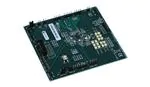
TPS6507xEVM
This user’s guide describes the characteristics, operation, and use of the TPS6507xEVM-430 evaluation
module (EVM). The TPS6507xEVM-430 is a fully assembled and tested platform for evaluating the
performance of the TPS6507x single-chip power management devices. This document includes schematic
diagrams, a printed circuit board (PCB) layout, bill of materials, and test data. Throughout this document,
the abbreviations EVM, TPS6507xEVM, and the term evaluation module are synonymous with the
TPS6507xEVM-430 unless otherwise noted.
1
2
3
4
5
6
7
Contents
Introduction .................................................................................................................. 2
TPS6507xEVM Electrical Performance Specifications ................................................................. 4
TPS6507xEVM Schematic ................................................................................................. 6
Connector and Test Point Descriptions .................................................................................. 8
Setup ........................................................................................................................ 12
EVM Assembly Drawings and Layout .................................................................................. 13
Bill of Materials ............................................................................................................. 19
List of Figures
1
TPS6507xEVM Schematic (Sheet 1) ..................................................................................... 6
2
TPS6507xEVM Schematic (Sheet 2) ..................................................................................... 7
3
TPS6507xEVM Hardware Connection.................................................................................. 12
4
TPS6507xEVM Component Placement (Viewed from Top) ......................................................... 13
5
TPS6507xEVM Silkscreen (Viewed from Top) ........................................................................ 14
6
TPS6507xEVM Top Copper (Viewed from Top) ...................................................................... 15
7
TPS6507xEVM Bottom Copper (X-Ray View from Top) ............................................................. 16
8
TPS6507xEVM Internal 1 (X-Ray View from Top) .................................................................... 17
9
TPS6507xEVM Internal 2 (X-Ray View from Top) .................................................................... 18
List of Tables
1
2
3
....................................................................................
TPS6507xEVM Performance Characteristics ...........................................................................
TPS65070EVM-430 Bill of Materials ...................................................................................
TPS6507xEVM Ordering Information
3
4
19
OMAP is a trademark of Texas Instruments.
Microsoft, Windows are registered trademarks of Microsoft Corporation.
I2C is a trademark of NXP Semiconductors.
All other trademarks are the property of their respective owners.
SLVU291B – April 2010 – Revised September 2011
Submit Documentation Feedback
Copyright © 2010–2011, Texas Instruments Incorporated
TPS6507xEVM
1
�Introduction
1
www.ti.com
Introduction
The TPS6507x are a series of single-chip power management ICs for portable applications consisting of a
battery charger with Power Path management for a single lithium-ion (Li-Ion) or lithium-polymer
(Li-Polymer) cell. The charger can be supplied either by a USB port on the device USB pin or by a dc
voltage from a wall adapter connected to the device AC pin. Three highly-efficient, 2.25-MHz step-down
converters provide the core voltage, memory, and input/output (I/O) voltage in a processor-based system.
The step-down converters enter a low-power mode under light loads for maximum efficiency across the
widest possible range of load currents. In addition, there are two 200-mA low-dropout regulators (LDOs).
For low-noise applications, these devices can be forced into fixed-frequency PWM using the I2C™
interface. The I2C interface allows the user to adjust various settings of the charger, the Power Path, the
dc-to-dc converters, and the LDOs. The step-down converters allow the use of small inductors and
capacitors in order to achieve a small total solution size.
1.1
Features
•
•
•
•
•
•
•
•
1.2
Applications
•
•
•
2
Battery charger with Power Path management
Up to 2.0-A output current on the Power Path
Three step-down converters
Two LDOs (200-mA output current)
wLED boost converter
Up to 25 mA per string with internal current sink
10-Bit analog-to-digital converter (ADC)/Touch screen interface
I2C-compatible interface
Portable navigation systems
PDAs, pocket PCs
OMAP™ and low-power DSP supply
TPS6507xEVM
SLVU291B – April 2010 – Revised September 2011
Submit Documentation Feedback
Copyright © 2010–2011, Texas Instruments Incorporated
�Introduction
www.ti.com
1.3
Requirements
In order to operate this EVM properly, the related software and hardware must be connected and properly
configured. All components and connectors are installed on the EVM as shipped, except for the host
computer and the dc power supply.
The most current version of the software must be downloaded from the TI website at www.ti.com.
1.3.1
Software
To download the software that is necessary to operate the TPS6507xEVM, check the TPS6507x product
folder on the TI Web site.
1.3.2
Host Computer
A computer with an available USB port is required to operate this EVM. The TPS6507xEVM software runs
on the personal computer and communicates with the EVM via the PC USB port and the USB to GPIO
interface. The PC must meet these minimum system requirements:
• Microsoft® Windows® 2000 or XP operating system
• Available USB port
• Minimum of 30 MB of free hard disk space (100 MB recommended)
• Minimum of 256 MB of RAM
1.3.3
Power Supply
A dc power supply capable of delivering 5 V at 3 A is required to operate this EVM.
1.3.4
Ordering Options
Table 1 provides the ordering information for the various EVM options.
Table 1. TPS6507xEVM Ordering Information
Output Voltage
Output Voltage
Output Current
LDO1 / LDO2
DCDC1 / DCDC2 /
DCDC3
Supported
Processor
3.3 V
1.8 V / 3.3 V
1.0 V / 1.2 V
1.8 V / 1.2 V
0.6 A / 1.5 A / 1.5 A
OMAP-L1x8
TPS65072
1.8 V / 1.2 V
1.2 V / 1.2 V
0.6 A / 0.6 A / 0.6 A
Atlas IV
TPS65073
1.8 V
1.2 V / 1.8 V
1.2 V / 1.35 V
1.8 V / 1.8 V
0.6 A / 0.6 A / 1.5 A
OMAP35xx
TPS650731EVM-430
TPS650731
1.8 V
1.2 V / 1.8 V
1.2 V / 1.35 V
1.8 V / 1.8 V
0.6 A / 0.6 A / 1.5 A
OMAP35xx
TPS650732EVM-430
TPS650732
1.8 V
1.8 V / 3.3 V
1.2 V / 1.35 V
1.8 V / 1.8 V
0.6 A / 0.6 A / 1.5 A
OMAP3505
Orderable EVM Number
Device Part
Number
DCDC1 / DCDC2
/ DCDC3
TPS65070EVM-430
TPS65070
TPS65072EVM-430
TPS65073EVM-430
SLVU291B – April 2010 – Revised September 2011
Submit Documentation Feedback
Copyright © 2010–2011, Texas Instruments Incorporated
TPS6507xEVM
3
�TPS6507xEVM Electrical Performance Specifications
2
www.ti.com
TPS6507xEVM Electrical Performance Specifications
Table 2 summarizes the TPS65070EVM-430 performance specifications.
Table 2. TPS6507xEVM Performance Characteristics
Parameter
Symbol
Notes and Conditions
Min
Nom
Max
Units
Input Characteristics
Input Voltage, AC
Input Voltage, USB
VAC
4.3
17
V
VUSB
4.3
5.8
V
4.3
5.8
V
VIN_DCDC
2.8
6.3 (1)
V
VIN_LDO
1.8
6.3 (1)
V
Input Voltage, AC, USB
charging
Input Voltage, DCDC1,
DCDC2, DCDC3
Input Voltage, LDO1, LDO2
Output Characteristics
DCDC1
Default Output Voltage
DCDC1
VOUT_DCDC1
TPS65070, TPS65072
3.3
V
Default Output Voltage
DCDC1
VOUT_DCDC1
TPS65073, TPS650731, TPS650732
1.8
V
Output Voltage Range
DCDC1
Adjustable with I2C
Output Current DCDC1
VIN = Min to max
3.3V or VIN_DCDC
(whichever is less)
0.725
V
600
mA
DEFDCDC2 = Low
1.8
V
DEFDCDC2 =
High
3.3
V
DEFDCDC2 = Low
1.8
V
DEFDCDC2 =
High
2.5
V
DEFDCDC2 = Low
1.2
V
DEFDCDC2 =
High
1.8
DCDC2
VOUT_DCDC2
Default Output Voltage
DCDC2
TPS65070,
TPS650732
VOUT_DCDC2
TPS65072
VOUT_DCDC2
TPS65073,
TPS650731
V
Output Voltage Range
DCDC2
3.3V or VIN_DCDC
(whichever is less)
Adjustable with I2C
TPS65072, TPS65073, TPS650731,
TPS650732
600
mA
Output Current DCDC2
TPS65070
1500
mA
0.725
V
DCDC3
DEFDCDC3 = Low
VOUT_DCDC3
Default Output Voltage
DCDC3
Output Current DCDC2
(1)
4
1
V
DEFDCDC3 =
High
1.2
V
DEFDCDC3 = Low
1.2
V
DEFDCDC3 =
High
1.4
V
DEFDCDC3 = Low
1.2
V
DEFDCDC3 =
High
1.35
V
TPS65072
600
mA
TPS65070, TPS65073, TPS650731,
TPS650732
1500
mA
TPS65070
VOUT_DCDC3
TPS65072
VOUT_DCDC3
TPS65073,
TPS650731,
TPS650732
6.3 V or VSYS, whichever is less.
TPS6507xEVM
SLVU291B – April 2010 – Revised September 2011
Submit Documentation Feedback
Copyright © 2010–2011, Texas Instruments Incorporated
�TPS6507xEVM Electrical Performance Specifications
www.ti.com
Table 2. TPS6507xEVM Performance Characteristics (continued)
Parameter
Symbol
Notes and Conditions
Min
Nom
Max
Units
LDO1, LDO2
Default Output Voltage LDO1,
LDO2
Default Output Voltage LDO2,
LDO2
TPS65070
1.8
mA
TPS65072
1.2
mA
TPS65073, TPS650731, TPS650732
1.8
mA
TPS65070
1.2
mA
TPS65072
1.2
mA
TPS65073, TPS650731, TPS650732
1.8
Output Current LDO1, LDO2
mA
200
mA
wLED Boost Converter and Current Sinks
Switching frequency wLED
boost
1125
Input voltage at ISINK1 , ISINK2
kHz
16
V
39
V
Internal overvoltage
protection
35
37
Maximum boost factor
(VIN/VOUT)
9
10
V
PWM dimming resolution
1
%
Tolerance between current sinks ISINK1, ISINK2
5
%
ADC Converter
Input voltage range AD_IN1
to AD_IN4
0
2.25
V
ADC resolution
10
Bits
Differential linearity error
±1
LSB
Offset error
1
Gain error
±8
LSB
Sampling rime
220
µs
Conversion time
19
µs
Reference voltage on
BYPASS
–1
5
LSB
2.26
+1
%
6.0
6.3
V
TSW(ACBAT)
200
µs
Switching from USB to BAT
TSW(USBBAT)
200
µs
Switching from AC to USB
TSW(ACUSB)
200
µs
Power Path
Minimum battery voltage
Input overvoltage protection
Switching from AC to BAT
VBATMIN
2.75
V(OVP)
5.8
V
SYS power-up delay
From power applied to start of power-up
sequence
11
ms
Dropout voltage AC to SYS
ILIMITAC = 2500 mA, ISYS = 1000 mA
150
mV
Dropout voltage USB to SYS
ILIMITUSB = 13000 mA, ISYS = 800 mA
160
Dropout voltage USB to SYS
VBAT = 3.0 V, ISYS = 1000 mA
85
mV
100
mV
2
A
Charger
Battery discharge current
Battery charge voltage
Set in internal register
4.1
4.25
V
Battery fast-charge current
range
Set with external resistor
100
1500
mA
Pre-charge current
Charge termination current
Switching frequency
IPRECHG
0.08 × ICHG
0.10 × ICHG
0.12 × ICHG
ITERM
0.08 × ICHG
0.10 × ICHG
0.12 × ICHG
1950
2250
2550
fSW
SLVU291B – April 2010 – Revised September 2011
Submit Documentation Feedback
Copyright © 2010–2011, Texas Instruments Incorporated
kHz
TPS6507xEVM
5
�TPS6507xEVM Schematic
3
www.ti.com
TPS6507xEVM Schematic
Figure 1 and Figure 2 show the two sheets of the TPS65070EVM-430 schematic.
NOTE: These diagrams are provided for reference only. See Table 3, the Bill of Materials, for
specific component values.
Figure 1. TPS6507xEVM Schematic (Sheet 1)
6
TPS6507xEVM
SLVU291B – April 2010 – Revised September 2011
Submit Documentation Feedback
Copyright © 2010–2011, Texas Instruments Incorporated
�TPS6507xEVM Schematic
www.ti.com
Figure 2. TPS6507xEVM Schematic (Sheet 2)
SLVU291B – April 2010 – Revised September 2011
Submit Documentation Feedback
Copyright © 2010–2011, Texas Instruments Incorporated
TPS6507xEVM
7
�Connector and Test Point Descriptions
www.ti.com
4
Connector and Test Point Descriptions
4.1
Input / Output Connector Descriptions
4.1.1
J1: VINLDO1, 2, GND
J1 pin 1 is the input supply for LDO1 and LDO2. In the default configuration, VINLDO1,2 is connected to
SYS with R1. To connect VINLDO1,2 to any other voltage source, remove R1 and connect the
VINLDO1,2 supply between J1 pin 1 (positive connection) and J1 pin 2 (GND connection).
4.1.2
J2: AC, GND
A power supply can be connected between J2 pin 1 (AC) and J2 pin 2 (GND). The AC pin is one of the
EVM inputs. Note that the voltage rating on the AC pin ranges from 4.3 V up to 17 V. The allowable
voltage range on both the AC and USB pins for charging is from 4.3 V up to 5.8 V. If the voltage on the
AC pin exceeds 5.8 V, the charger goes into overvoltage lockout.
The input current on the Power Path input AC pin is current-limited. The current limit can be changed in
User Register PPATH1 (01h). The default input current limit is set to 2500 mA. For more information, refer
to the respective device data sheet, available for download at www.ti.com.
4.1.3
J3: USB, GND
Connect your power supply positive terminal to J3 pin 1. Connect your power supply negative terminal to
J3 pin 2. Note that the voltage rating on the USB input ranges from 4.3 V up to 17 V. The allowable
voltage range on both the AC and USB pins for charging is from 4.3 V up to 5.8 V. If the voltage on the
AC pin exceeds 5.8 V, the charger goes into overvoltage lockout.
The input current on the Power Path input USB pin is current-limited. The current limit can be changed in
User Register PPATH1 (01h). The default input current limit is set to 500 mA. For more information, refer
to the respective device data sheet, available for download at www.ti.com.
4.1.4
J4: SYS
J4 is connected to the output of the Power Path (SYS). When the TPS6507x device is turned off and there
is no voltage source applied at either the AC or USB pins, the SYS output is disconnected internally from
the battery. When the TPS6507x is turned on by pulling PB_IN low, the voltage at SYS ramps up. If there
is no voltage applied at either the AC or USB pin, SYS remains connected to VBAT internally. If there is a
voltage applied at either the AC or USB pin, SYS is connected to this input. If both input supplies are
connected, the AC input has priority. The voltage at SYS is not regulated.
4.1.5
J5: GND
J5 is connected to GND.
4.1.6
J6: VBAT, GND, TS
Connect your single-cell Li-Ion or Li-Polymer cell positive connection to J6 pins 1 and 2. Connect your
battery negative connection between J6 pins 3 and 4. If your battery provides a thermistor (NTC)
connection, you can connect the thermistor to J6 pin 5. Note that the factory default EVM configuration
includes a 10-kΩ resistor connected from TS to GND (R5). If you wish to use the battery internal resistor,
R5 must first be removed. The thermistor type is defined in User Register CHGCONFIG1 with the bit
SENSOR TYPE. Two different thermistor types can be selected: 100 kΩ and 10 kΩ; the default selection
is 10 kΩ.
A resistor in parallel to the thermistor (NTC) is required for linearization (see the TPS6507x data sheet for
details). Note that the factory default EVM configuration uses a 75-kΩ resistor for linearization (R6).
8
TPS6507xEVM
SLVU291B – April 2010 – Revised September 2011
Submit Documentation Feedback
Copyright © 2010–2011, Texas Instruments Incorporated
�Connector and Test Point Descriptions
www.ti.com
4.1.7
J7: VLDO1, GND
J7 pins 1 and 2 are connected to the positive output of linear regulator LDO1. J7 pins 2 and 4 are the
GND connection for LDO1. A load can be connected between J7 pins 1 and 2 (VLDO1) and J13 pins 3
and 4 (GND).
LDO1 is able to supply a load current up to 200 mA.
4.1.8
J8: VLDO2, GND
J8 pins 1 and 2 are connected to the positive output of linear regulator LDO2. J8 pins 2 and 4 are the
GND connection for LDO2. A load can be connected between J8 pins 1 and 2 (VLDO2) and J8 pins 3 and
4 (GND).
LDO2 is able to supply a load current up to 200 mA.
4.1.9
J9: VDCDC1, GND
J9 pins 3 and 4 are connected to the positive output of the step-down converter DCDC1. J9 pins 1 and 2
are the GND connection of DCDC1. A load can be connected between J9 pins 3 and 4 (VDCDC1) and J9
pins 1 and 2 (GND).
Refer to Table 2 for information on the maximum output current and default output voltage of DCDC1.
4.1.10
J10: VDCDC2, GND
J10 pins 3 and 4 are connected to the positive output of the step-down converter DCDC2. J10 pins 1 and
2 are the GND connection of DCDC2. A load can be connected between J10 pins 3 and 4 (VDCDC2) and
J10 pins 1 and 2 (GND).
Refer to Table 2 for information on the maximum output current and default output voltage of DCDC2.
4.1.11
J11: VDCDC3, GND
J11 pins 3 and 4 are the positive output of the step-down converter DCDC3. J11 pins 1 and 2 are the
GND connection of DCDC3. A load can be connected between J11 pins 3 and 4 (VDCDC3) and J11 pins
1 and 2 (GND).
Refer to Table 2 for information on the maximum output current and default output voltage of DCDC3.
4.1.12
J12: I2C Interface
J12 is a 10-pin interface connector to connect to the I2C interface.
4.1.13
J13: I2C Interface
J13 is a 14-pin interface connector to connect to the I2C interface. This connector is not assembled in the
factory default EVM setup.
4.1.14
J14: AD_IN1–4, BYPASS, INT_LDO, GND
AD_IN1, AD_IN2, AD_IN3, and AD_IN4 are the external inputs of the 10-bit ADC. Connect an external
voltage source or touch screen (If configured as touch screen controller) to these pins. See the respective
device data sheet for additional information on the touch screen interface and ADC input configuration.
J14 pin 5 is connected to BYPASS. BYPASS can be used as an internal reference for the ADC. A 10-µF
capacitor is connected from BYPASS to GND (C10).
J14 pin 6 is connected to the output of the internal LDO, INT_LDO. This LDO provides power for the touch
screen controller (TSREF). A 2.2-µF capacitor is connected from INT_LDO to GND (C13).
SLVU291B – April 2010 – Revised September 2011
Submit Documentation Feedback
Copyright © 2010–2011, Texas Instruments Incorporated
TPS6507xEVM
9
�Connector and Test Point Descriptions
4.1.15
www.ti.com
J15: PB_IN, PB_OUT, POWER_ON, PGOOD, RESET/EN_EXTLDO, INT
J15, pin 1: PB_IN
J15 pin 1 is connected to PB_IN. Pulling PB_IN low starts up all dc-dc converters and LDOs according
to the internal power-up sequence. Refer to Table 9 in the data sheet (SLVS950) for information on the
internal power-up sequence. Note that if PB_IN is released high, all dc-dc converters and LDOs shut
down if the POWER_ON input is low. If POWER_ON is pulled high before PB_IN is released high
again, the dc-dc converters and LDOs remain on. Note that PB_IN is also connected to S1. PB_IN is
pulled up to AVDD6 with an internal 50-kΩ pull-up resistor. Pressing the Push-Button S1 pulls PB_IN
low.
J15, pin 2: PB_OUT
J15 pin 2 is connected to the open drain output PB_OUT. PB_OUT is driven by the status of PB_IN. If
PB_IN is low, PB_OUT is also low. If PB_IN is high, PB_OUT is driven to a high impedance state.
PB_OUT is pulled up to a pull-up voltage with resistor R37. In the factory default configuration, VSYS
is selected as the pull-up voltage. In addition, VOUT_DCDC1 and VOUT_DCDC2 can be configured as
pull-up voltages with R22 and R23, respectively.
J15, pin 3: POWER_ON
The POWER_ON pin must be pulled high before PB_IN is released high again to keep the dc-dc
converters and LDOs enabled once PB_IN is released high. Pulling POWER_ON low disables all dc-dc
converters and LDOs. POWER_ON is pulled up to a pull-up voltage with R32. In the factory default
configuration, VSYS is selected as the pull-up voltage. In addition, VOUT_DCDC1 and VOUT_DCDC2
can be configured as pull-up voltages with R22 and R23, respectively.
J15, pin 4: PGOOD
J15 pin 4 is connected to the open drain output PGOOD. PGOOD goes low depending on the setting
in the PGOODMASK register. In this register, different PGOOD bits of each dc-dc converter and LDO
can be connected to the PGOOD open drain output. PGOOD is connected to a pull-up voltage with
resistor R34. In the factory default EVM configuration, VSYS is selected as the pull-up voltage with
R21. In addition, VOUT_DCDC1 and VOUT_DCDC2 can be configured as pull-up voltages with R22
and R23, respectively.
J15, pin 6: RESET/EN_EXTLDO
J15 pin 5 is connected to the open drain output RESET. The TPS65070, TPS65073, TPS650731, and
TPS650732 each contain circuitry that can generate a reset pulse for a processor. The voltage at the
THRESHOLD pin is sensed; if this voltage goes above the threshold voltage of 1.0 V (typ), the RESET
output goes to a high impedance state after a delay time defined in the PGOOD register. If the voltage
at the THRESHOLD pin is below the threshold voltage, the PGOOD output is pulled low.
In the TPS65072, this pin is an active high push-pull output called EN_EXTLDO. This pin is controlled
internally and only used for sequencing the Sirf Prima or Atlas IV processors.
J15, pin 6: INT
J15 pin 6 is connected to the open drain output INT. The INT output indicates if there is an interrupt
active. The interrupts can be configured in the INT register. Different events can be masked as an
interrupt (for example, AC pin or USB pin power removed or applied), or as a touch screen Interface,
PB_IN.
INT is connected to a pull-up voltage with resistor R38. In the factory default EVM configuration, VSYS
is selected as the pull-up voltage with R21. In addition, VOUT_DCDC1 and VOUT_DCDC2 can be
configured as pull-up voltages with R22 and R23, respectively.
10
TPS6507xEVM
SLVU291B – April 2010 – Revised September 2011
Submit Documentation Feedback
Copyright © 2010–2011, Texas Instruments Incorporated
�Connector and Test Point Descriptions
www.ti.com
4.2
4.2.1
Enable Jumpers / Switches
S1: PB_IN
S1 is connected to PB_IN. Pressing the switch S1 pulls the PB_IN pin of the TPS6507x low, starting up all
dc-dc converters and LDOs according to the device internal sequence. Note that if S1 is released, all
dc-dc converters and LDOs shut down if the POWER_ON input is low. If POWER_ON is pulled high
before PB_IN is released high again, the dc-dc converters and LDOs remain on.
JP1: EN_DCDC1
Connect a shorting bar between EN_DCDC1 and ON to pull the EN_DCDC1 pin high (VSYS) and
enable the step-down converter DCDC1. Connect a shorting bar between EN_DCDC1 and OFF to pull
the EN_DCDC1 pin low (GND) and disable DCDC1.
Note that the enable pins of all dc-dc converters and LDOs that are part of the internal automatic
sequence should be terminated to GND. To control the converters with the respective individual
ENABLE pins, the power sequence for the dc-dc converters DCDC_SQ must be set to '101' in User
Register CON_CTRL1 (0Dh).
JP2: EN_DCDC2
Connect a shorting bar between EN_DCDC2 and ON to pull the EN_DCDC2 pin high (VSYS) and
enable the step-down converter DCDC2. Connect a shorting bar between EN_DCDC2 and OFF to pull
the EN_DCDC2 pin low (GND) and disable DCDC2.
Note that the enable pins of all dc-dc converters and LDOs that are part of the internal automatic
sequence should be terminated to GND. To control the converters with the respective individual
ENABLE pins, the power sequence for the dc-dc converters DCDC_SQ must be set to '101' in User
Register CON_CTRL1 (0Dh).
JP3: EN_DCDC3
Connect a shorting bar between EN_DCDC3 and ON to pull the EN_DCDC3 pin high (VSYS) and
enable the step-down converter DCDC3. Connect a shorting bar between EN_DCDC3 and OFF to pull
the EN_DCDC3 pin low (GND) and disable DCDC3.
Note that the enable pins of all dc-dc converters and LDOs that are part of the internal automatic
sequence should be terminated to GND. To control the converters with the respective individual
ENABLE pins, the power sequence for the dc-dc converters DCDC_SQ must be set to '101' in User
Register CON_CTRL1 (0Dh).
JP4: DEFDCDC2
Connecting a shorting bar between DEFDCDC2 and LOW selects the output voltage set in User
Register DEFDCDC2_LOW (11h). Connecting a shorting bar between DEFDCDC2 and HIGH selects
the output voltage set in User Register DEFDCDC2_HIGH (12h).
Refer to Table 2 for information on the default output voltages on DCDC2. After start-up, the user can
adjust the LOW/HIGH output voltage of DCDC2 in the corresponding User Registers. Refer to the
device data sheet for detailed information.
JP5: DEFDCDC3
Connecting a shorting bar between DEFDCDC3 and LOW selects the output voltage set in the User
Register DEFDCDC3_LOW (13h). Connecting a shorting bar between DEFDCDC3 and HIGH selects
the output voltage set in the User Register DEFDCDC3_HIGH (14h).
Refer to Table 2 for information on the default output voltages on DCDC3. After start-up, the user can
adjust the LOW/HIGH output voltage of DCDC3 in the corresponding User Registers. Refer to the
device data sheet for detailed information.
JP6: POWER_ON
The POWER_ON pin must be pulled high before PB_IN is released high again to keep the dc-dc
converters and LDOs enabled once PB_IN is released high. Pulling POWER_ON low disables all dc-dc
converters and LDOs. Connect a shorting bar between POWER_ON and Hi to pull the POWER_ON
pin high. The pull-up source can be selected with resistors R45 (VDCDC2), R46 (VDCDC1) and R47
(SYS). In the factory default configuration, R45 and R46 are open, while R47 is assembled. This
configuration selects SYS as the pull-up source. Connect a shorting bar between POWER_ON and
GND to pull the POWER_ON pin low. This configuration disables all dc-dc converters and LDOs.
SLVU291B – April 2010 – Revised September 2011
Submit Documentation Feedback
Copyright © 2010–2011, Texas Instruments Incorporated
TPS6507xEVM
11
�Setup
5
www.ti.com
Setup
CAUTION
Many of the components on the TPS6507xEVM-430 are susceptible to damage
by electrostatic discharge (ESD). Customers are advised to observe proper
ESD handling precautions when unpacking and handling the EVM, including
the use of a grounded wrist strap, bootstraps, or mats at an approved ESD
workstation. An electrostatic smock and safety glasses should also be worn.
5.1
Software Setup
To download the software required to operate the TPS6507xEVM, check the TPS6507x product folder on
the TI web site (www.ti.com).
Download the software and execute it; follow the on-screen instructions to complete the installation.
5.2
Hardware Setup
Figure 3 shows a typical hardware test configuration.
Lithium-Ion
Battery
LDO2
DCDC3
J11
LDO1
J8
J6
TS - +
TPS6507xEVM-430
Oscilloscope
DC Voltmeter
+
J2
AC
DC
Power Supply
-
J3
USB
J13
J9
J10
DCDC1
DCDC2
PC
USB to GPIO Interface
Figure 3. TPS6507xEVM Hardware Connection
5.3
Running the Software
Click on the TPS6507x software icon to start the software. If no icon appears on the host computer
desktop, use the Start button in the lower left corner of the screen to browse the program folders to find
the installed software. The default directory for the software installation is Program Files\Texas
Instruments\TPS6507xEVM.
For details on how to use the software, refer to application note SLVA418, Using the TPS6507x Software.
12
TPS6507xEVM
SLVU291B – April 2010 – Revised September 2011
Submit Documentation Feedback
Copyright © 2010–2011, Texas Instruments Incorporated
�EVM Assembly Drawings and Layout
www.ti.com
6
EVM Assembly Drawings and Layout
Figure 4 through Figure 9 show the design of the TPS65070EVM-430 printed circuit boards. This EVM
has been designed using a four-layer, 1-ounce copper-clad PCB with all components in an active area on
the top side of the board.
NOTE: Board layouts are not to scale. These figures are intended to show how the board is laid out;
they are not intended to be used for manufacturing TPS65070EVM-430 PCBs.
Figure 4. TPS6507xEVM Component Placement (Viewed from Top)
SLVU291B – April 2010 – Revised September 2011
Submit Documentation Feedback
Copyright © 2010–2011, Texas Instruments Incorporated
TPS6507xEVM
13
�EVM Assembly Drawings and Layout
www.ti.com
TEXAS
INSTRUMENTS
HPA 430 Rev. A
Figure 5. TPS6507xEVM Silkscreen (Viewed from Top)
14
TPS6507xEVM
SLVU291B – April 2010 – Revised September 2011
Submit Documentation Feedback
Copyright © 2010–2011, Texas Instruments Incorporated
�EVM Assembly Drawings and Layout
www.ti.com
Figure 6. TPS6507xEVM Top Copper (Viewed from Top)
SLVU291B – April 2010 – Revised September 2011
Submit Documentation Feedback
Copyright © 2010–2011, Texas Instruments Incorporated
TPS6507xEVM
15
�EVM Assembly Drawings and Layout
www.ti.com
Figure 7. TPS6507xEVM Bottom Copper (X-Ray View from Top)
16
TPS6507xEVM
SLVU291B – April 2010 – Revised September 2011
Submit Documentation Feedback
Copyright © 2010–2011, Texas Instruments Incorporated
�EVM Assembly Drawings and Layout
www.ti.com
Figure 8. TPS6507xEVM Internal 1 (X-Ray View from Top)
SLVU291B – April 2010 – Revised September 2011
Submit Documentation Feedback
Copyright © 2010–2011, Texas Instruments Incorporated
TPS6507xEVM
17
�EVM Assembly Drawings and Layout
www.ti.com
Figure 9. TPS6507xEVM Internal 2 (X-Ray View from Top)
18
TPS6507xEVM
SLVU291B – April 2010 – Revised September 2011
Submit Documentation Feedback
Copyright © 2010–2011, Texas Instruments Incorporated
�Bill of Materials
www.ti.com
7
Bill of Materials
Table 3 lists the bill of materials for the TPS6507xEVM.
Table 3. TPS65070EVM-430 Bill of Materials
EVM Device Option: Count
-001
-002
-003
-004
-005
RefDes
Value
Description
Size
Part Number
MFR
2.2 µF
Capacitor, Ceramic,
6.3 V, X5R, 10%
0805
GRM21BR60J225KA01K
muRata
4
4
4
4
4
C1, C13,
C17, C18
0
0
0
0
0
C19, C20,
C21
open
Capacitor, Ceramic,
6.3 V, X5R, 20%
0805
JMK212BJ106M
Taiyo
Yuden
1
1
1
1
1
C2
4.7 µF
Capacitor, Ceramic,
50 V, X7R, 10%
1210
GRM32ER71H475KA
Taiyo
Yuden
4
4
4
4
4
C22, C23,
C24, C25
10nF
Capacitor, Ceramic,
100 V, X7R, 20%
0805
GRM21BR72A103MA01K
muRata
3
3
3
3
3
C3, C4,
C11
4.7 µF
Capacitor, Ceramic,
6.3 V, X5R, 10%
0805
GRM21BR60J475KA11K
muRata
7
7
7
7
7
C5, C7,
C10, C12,
C14, C15,
C16
10 µF
Capacitor, Ceramic,
6.3 V, X5R, 20%
0805
JMK212BJ106M
Taiyo
Yuden
2
2
2
2
2
C6, C8
22 µF
Capacitor, Ceramic,
6.3 V, X5R, 20%
0805
JMK212BJ226MG
muRata
0
0
0
0
0
C9
open
1
1
1
1
0805
muRata
1
D1
MBR0540L
Diode, Schottky,
0.5 A, 20 V
Q65110A1931
Diode, LED, 30-mA,
Common Anode
0.118 x
0.134 inch
Q65110A1931
Osram
SOD-123
MBR0520L
Fairchild
16
16
16
16
16
D2, D3,
D4, D5,
D6, D7,
D8, D9,
D10, D11,
D12, D13,
D14, D15,
D16, D17
1
1
1
1
1
L1
47 µH
Inductor, SMT,
0.56 A, 650 mΩ
0.153 x
0.153 inch
LPS4018-473MLB
Coilcraft
3
3
3
3
3
L2, L3, L4
2.2 µH
Inductor, SMT,
2.1 A, 110 mΩ
0.118 x
0.118 inch
LPS3015-222ML
Coilcraft
0
0
0
0
0
Q1
open
MOSFET, Pch, -12 V,
–5.7 A, 50 mΩ
SOT23
Si2333
Vishay
8
8
8
8
8
R1, R7,
R13, R18,
R19, R20,
R21, R26
0
Resistor, Chip,
1/10W, 1%
0805
Std
Std
1
0
1
1
1
R36
0
Resistor, Chip,
1/10W, 1%
0805
Std
Std
2
2
2
2
2
R14, R16
3.30 kΩ
Resistor, Chip,
1/10W, 1%
0805
Std
Std
1
1
1
1
1
R2
51.1 kΩ
Resistor, Chip, 1/10W,
1%
0805
Std
Std
4
4
4
4
4
R24, R25,
R27, R28
1.00 MΩ
Resistor, Chip,
1/10W, 1%
0805
Std
Std
1
1
1
1
1
R3
1.00 kΩ
Resistor, Chip,
1/10W, 1%
0805
Std
Std
0
1
0
0
0
R31
0Ω
Resistor, Chip,
1/10W, 1%
0805
Std
Std
1
0
1
1
1
R31
270 kΩ
Resistor, Chip,
1/10W, 1%
0805
Std
Std
4
4
4
4
4
R32, R33,
R37, R38
100 kΩ
Resistor, Chip,
1/10W, 1%
0805
Std
Std
1
0
1
1
1
R34
100 kΩ
Resistor, Chip,
1/10W, 1%
0805
Std
Std
1
0
1
1
1
R35
120 kΩ
Resistor, Chip,
1/10W, 1%
0805
Std
Std
1
1
1
1
1
R4
150 kΩ
Resistor, Chip,
1/10W, 1%
0805
Std
Std
SLVU291B – April 2010 – Revised September 2011
Submit Documentation Feedback
Copyright © 2010–2011, Texas Instruments Incorporated
TPS6507xEVM
19
�Revision History
www.ti.com
Table 3. TPS65070EVM-430 Bill of Materials (continued)
EVM Device Option: Count
-001
-002
-003
-004
-005
RefDes
Value
Description
Size
Part Number
MFR
0805
Std
Std
1
1
1
1
1
R5
10.0 KΩ
Resistor, Chip,
1/10W, 1%
1
1
1
1
1
R6
75.0 kΩ
Resistor, Chip,
1/10W, 1%
0805
Std
Std
open
Resistor, Chip,
1/10W, 1%
0805
Std
Std
KT11P2JM
Switch, SPST,
PB Momentary, Sealed
Tactile
0.245 X
0.251 inch
KT11P2JM34LFS
KT11P2J
M34LFS
0
0
0
0
0
R8, R9,
R10, R11,
R12, R15,
R17, R22,
R23, R29,
R30
1
1
1
1
1
S1
1
0
0
0
0
TPS65070RSL
IC, Power Solution for
Navigation Systems
TPS65070RSL
TI
0
1
0
0
0
TPS65072RSL
IC, Power Solution for
Navigation Systems
TPS65072RSL
TI
0
0
1
0
0
TPS65073RSL
IC, Power Solution for
Navigation Systems
TPS65073RSL
TI
0
0
0
1
0
TPS650731RSL
IC, Power Solution for
Navigation Systems
TPS650731RSL
TI
0
0
0
0
1
TPS650732RSL
IC, Power Solution for
Navigation Systems
TPS650732RSL
TI
Revision History
Changes from Original (April, 2010) to A Revision ......................................................................................................... Page
•
•
Updated Table 1 with correct maximum DC/DC2 output current
Updated Table 2 with correct maximum DC/DC2 output current
..................................................................
..................................................................
3
4
NOTE: Page numbers for previous revisions may differ from page numbers in the current version.
20
Revision History
SLVU291B – April 2010 – Revised September 2011
Submit Documentation Feedback
Copyright © 2010–2011, Texas Instruments Incorporated
�Evaluation Board/Kit Important Notice
Texas Instruments (TI) provides the enclosed product(s) under the following conditions:
This evaluation board/kit is intended for use for ENGINEERING DEVELOPMENT, DEMONSTRATION, OR EVALUATION
PURPOSES ONLY and is not considered by TI to be a finished end-product fit for general consumer use. Persons handling the
product(s) must have electronics training and observe good engineering practice standards. As such, the goods being provided are
not intended to be complete in terms of required design-, marketing-, and/or manufacturing-related protective considerations,
including product safety and environmental measures typically found in end products that incorporate such semiconductor
components or circuit boards. This evaluation board/kit does not fall within the scope of the European Union directives regarding
electromagnetic compatibility, restricted substances (RoHS), recycling (WEEE), FCC, CE or UL, and therefore may not meet the
technical requirements of these directives or other related directives.
Should this evaluation board/kit not meet the specifications indicated in the User’s Guide, the board/kit may be returned within 30
days from the date of delivery for a full refund. THE FOREGOING WARRANTY IS THE EXCLUSIVE WARRANTY MADE BY
SELLER TO BUYER AND IS IN LIEU OF ALL OTHER WARRANTIES, EXPRESSED, IMPLIED, OR STATUTORY, INCLUDING
ANY WARRANTY OF MERCHANTABILITY OR FITNESS FOR ANY PARTICULAR PURPOSE.
The user assumes all responsibility and liability for proper and safe handling of the goods. Further, the user indemnifies TI from all
claims arising from the handling or use of the goods. Due to the open construction of the product, it is the user’s responsibility to
take any and all appropriate precautions with regard to electrostatic discharge.
EXCEPT TO THE EXTENT OF THE INDEMNITY SET FORTH ABOVE, NEITHER PARTY SHALL BE LIABLE TO THE OTHER
FOR ANY INDIRECT, SPECIAL, INCIDENTAL, OR CONSEQUENTIAL DAMAGES.
TI currently deals with a variety of customers for products, and therefore our arrangement with the user is not exclusive.
TI assumes no liability for applications assistance, customer product design, software performance, or infringement of
patents or services described herein.
Please read the User’s Guide and, specifically, the Warnings and Restrictions notice in the User’s Guide prior to handling the
product. This notice contains important safety information about temperatures and voltages. For additional information on TI’s
environmental and/or safety programs, please contact the TI application engineer or visit www.ti.com/esh.
No license is granted under any patent right or other intellectual property right of TI covering or relating to any machine, process, or
combination in which such TI products or services might be or are used.
FCC Warning
This evaluation board/kit is intended for use for ENGINEERING DEVELOPMENT, DEMONSTRATION, OR EVALUATION
PURPOSES ONLY and is not considered by TI to be a finished end-product fit for general consumer use. It generates, uses, and
can radiate radio frequency energy and has not been tested for compliance with the limits of computing devices pursuant to part 15
of FCC rules, which are designed to provide reasonable protection against radio frequency interference. Operation of this
equipment in other environments may cause interference with radio communications, in which case the user at his own expense
will be required to take whatever measures may be required to correct this interference.
EVM Warnings and Restrictions
It is important to operate this EVM within the input voltage range of 3.6 V to 17 V and the output voltage range of 0.6 V to 6.3 V.
Exceeding the specified input range may cause unexpected operation and/or irreversible damage to the EVM. If there are
questions concerning the input range, please contact a TI field representative prior to connecting the input power.
Applying loads outside of the specified output range may result in unintended operation and/or possible permanent damage to the
EVM. Please consult the EVM User's Guide prior to connecting any load to the EVM output. If there is uncertainty as to the load
specification, please contact a TI field representative.
During normal operation, some circuit components may have case temperatures greater than +60°C. The EVM is designed to
operate properly with certain components above +60°C as long as the input and output ranges are maintained. These components
include but are not limited to linear regulators, switching transistors, pass transistors, and current sense resistors. These types of
devices can be identified using the EVM schematic located in the EVM User's Guide. When placing measurement probes near
these devices during operation, please be aware that these devices may be very warm to the touch.
Mailing Address: Texas Instruments, Post Office Box 655303, Dallas, Texas 75265
Copyright © 2011, Texas Instruments Incorporated
�IMPORTANT NOTICE
Texas Instruments Incorporated and its subsidiaries (TI) reserve the right to make corrections, modifications, enhancements, improvements,
and other changes to its products and services at any time and to discontinue any product or service without notice. Customers should
obtain the latest relevant information before placing orders and should verify that such information is current and complete. All products are
sold subject to TI’s terms and conditions of sale supplied at the time of order acknowledgment.
TI warrants performance of its hardware products to the specifications applicable at the time of sale in accordance with TI’s standard
warranty. Testing and other quality control techniques are used to the extent TI deems necessary to support this warranty. Except where
mandated by government requirements, testing of all parameters of each product is not necessarily performed.
TI assumes no liability for applications assistance or customer product design. Customers are responsible for their products and
applications using TI components. To minimize the risks associated with customer products and applications, customers should provide
adequate design and operating safeguards.
TI does not warrant or represent that any license, either express or implied, is granted under any TI patent right, copyright, mask work right,
or other TI intellectual property right relating to any combination, machine, or process in which TI products or services are used. Information
published by TI regarding third-party products or services does not constitute a license from TI to use such products or services or a
warranty or endorsement thereof. Use of such information may require a license from a third party under the patents or other intellectual
property of the third party, or a license from TI under the patents or other intellectual property of TI.
Reproduction of TI information in TI data books or data sheets is permissible only if reproduction is without alteration and is accompanied
by all associated warranties, conditions, limitations, and notices. Reproduction of this information with alteration is an unfair and deceptive
business practice. TI is not responsible or liable for such altered documentation. Information of third parties may be subject to additional
restrictions.
Resale of TI products or services with statements different from or beyond the parameters stated by TI for that product or service voids all
express and any implied warranties for the associated TI product or service and is an unfair and deceptive business practice. TI is not
responsible or liable for any such statements.
TI products are not authorized for use in safety-critical applications (such as life support) where a failure of the TI product would reasonably
be expected to cause severe personal injury or death, unless officers of the parties have executed an agreement specifically governing
such use. Buyers represent that they have all necessary expertise in the safety and regulatory ramifications of their applications, and
acknowledge and agree that they are solely responsible for all legal, regulatory and safety-related requirements concerning their products
and any use of TI products in such safety-critical applications, notwithstanding any applications-related information or support that may be
provided by TI. Further, Buyers must fully indemnify TI and its representatives against any damages arising out of the use of TI products in
such safety-critical applications.
TI products are neither designed nor intended for use in military/aerospace applications or environments unless the TI products are
specifically designated by TI as military-grade or "enhanced plastic." Only products designated by TI as military-grade meet military
specifications. Buyers acknowledge and agree that any such use of TI products which TI has not designated as military-grade is solely at
the Buyer's risk, and that they are solely responsible for compliance with all legal and regulatory requirements in connection with such use.
TI products are neither designed nor intended for use in automotive applications or environments unless the specific TI products are
designated by TI as compliant with ISO/TS 16949 requirements. Buyers acknowledge and agree that, if they use any non-designated
products in automotive applications, TI will not be responsible for any failure to meet such requirements.
Following are URLs where you can obtain information on other Texas Instruments products and application solutions:
Products
Applications
Audio
www.ti.com/audio
Communications and Telecom www.ti.com/communications
Amplifiers
amplifier.ti.com
Computers and Peripherals
www.ti.com/computers
Data Converters
dataconverter.ti.com
Consumer Electronics
www.ti.com/consumer-apps
DLP® Products
www.dlp.com
Energy and Lighting
www.ti.com/energy
DSP
dsp.ti.com
Industrial
www.ti.com/industrial
Clocks and Timers
www.ti.com/clocks
Medical
www.ti.com/medical
Interface
interface.ti.com
Security
www.ti.com/security
Logic
logic.ti.com
Space, Avionics and Defense
www.ti.com/space-avionics-defense
Power Mgmt
power.ti.com
Transportation and Automotive www.ti.com/automotive
Microcontrollers
microcontroller.ti.com
Video and Imaging
RFID
www.ti-rfid.com
OMAP Mobile Processors
www.ti.com/omap
Wireless Connctivity
www.ti.com/wirelessconnectivity
TI E2E Community Home Page
www.ti.com/video
e2e.ti.com
Mailing Address: Texas Instruments, Post Office Box 655303, Dallas, Texas 75265
Copyright © 2011, Texas Instruments Incorporated
�