User's Guide
SLVUAB3A – October 2014 – Revised February 2016
TPS65132W Evaluation Module
This user's guide describes the characteristics, operation, and use of the TPS65132W evaluation module
(EVM) and its software. It includes the EVM specifications, the recommended setup (hardware and
software), the schematic diagram, the board layouts, and the bill of materials.
All the measurements in the Application Performance section of the TPS65132W datasheet (SLVSBM1)
were done with this EVM.
1
2
3
4
5
6
7
8
Contents
Introduction ................................................................................................................... 2
Electrical Specifications ..................................................................................................... 3
Schematic ..................................................................................................................... 4
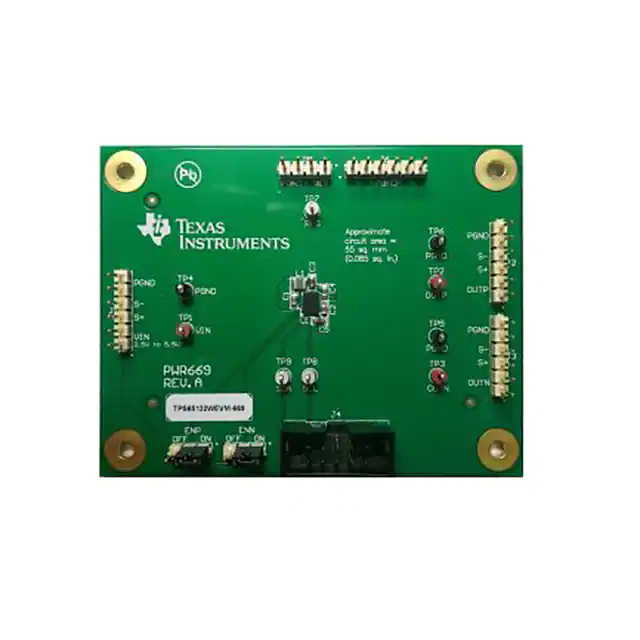
Connectors, Jumpers and Test Points .................................................................................... 5
Setup .......................................................................................................................... 6
Software Operation .......................................................................................................... 9
PCB Layout ................................................................................................................. 14
List of Materials ............................................................................................................. 16
List of Figures
1
Schematic ..................................................................................................................... 4
2
Hardware Setup – Full Functionality ...................................................................................... 6
3
Hardware Setup – Simplified ............................................................................................... 6
4
Two-Terminal Power Supply Connection ................................................................................. 7
5
Four-Terminal Power Supply Connection
6
7
8
9
10
11
12
13
14
15
16
17
................................................................................ 7
Single-Ended Load Connections .......................................................................................... 7
Differential Load Connection ............................................................................................... 8
Ribbon Cable Connected to the Ten Middle Pins of the USB2ANY Interface Adapter............................. 8
Device Selection Window ................................................................................................... 9
Settings Window ............................................................................................................. 9
I2C Bus Internal Pullup Connection ...................................................................................... 10
I2C Bus External Pullup Connection ..................................................................................... 10
DAC Registers Window ................................................................................................... 12
Demo Mode Prompt with No EVM Connected ......................................................................... 13
Component Placement (Top View) ...................................................................................... 14
PCB Top Layer (Top View) ............................................................................................... 14
PCB Bottom Layer (Bottom View) ....................................................................................... 15
List of Tables
1
Electrical Specifications ..................................................................................................... 3
2
Connector Overview ......................................................................................................... 5
3
Jumper Overview ............................................................................................................ 5
4
Test Point Overview ......................................................................................................... 5
5
Bill of Materials
.............................................................................................................
SLVUAB3A – October 2014 – Revised February 2016
Submit Documentation Feedback
Copyright © 2014–2016, Texas Instruments Incorporated
TPS65132W Evaluation Module
16
1
�Introduction
1
www.ti.com
Introduction
This EVM uses a TPS65132W to generate the positive and negative supply voltages needed by LCD
panels in smartphones and tablet PCs. It can also be used as a general-purpose power supply in
applications that need positive and negative supply rails (for example, op-amp or data acquisition circuits).
For easy performance evaluation of the TPS65132W, this EVM has:
• Software with a Graphical User Interface (GUI) for reading, writing, exporting, and importing the device
configuration
• A USB2ANY interface adapter to control the I2C bus
• Test points for measuring the most important voltages
• Jumpers for enabling and disabling the outputs
• Input and output voltage sense terminals for making accurate four-terminal voltage measurements
1.1
Recommended Equipment
In addition to the contents of the EVM box, some or all of the equipment described in the following
subsections is required.
1.1.1
Power Supply
To evaluate the full performance of the TPS65132W, a dc power supply capable of delivering 1.2 A from
2.5 V to 5.5 V is required.
1.1.2
Host Computer
To change the output voltages or configuration of the TPS65132W, a personal computer (PC) with the
following minimum specifications is needed:
• Microsoft® Windows® 7 operating system
• One free USB port
• A minimum of 280MB of free hard disk space (610MB recommended)
• A minimum of 512MB of RAM
1.1.3
Software
You can download the latest version of the EVM software from the TI website at
http://www.ti.com/product/tps65132 (see also Section 5.2).
1.2
Applications
The TPS65132W device is suitable for use in any applications that need positive and negative output
voltages in the range ±4 V to ±6 V and output currents less than ±80 mA. Typical applications include:
• Smartphone displays
• Tablet displays
• Split-rail power supply applications
Microsoft, Windows are registered trademarks of Microsoft Corporation.
2
TPS65132W Evaluation Module
SLVUAB3A – October 2014 – Revised February 2016
Submit Documentation Feedback
Copyright © 2014–2016, Texas Instruments Incorporated
�Introduction
www.ti.com
1.3
Features
•
•
•
•
•
•
•
•
•
•
2
Efficiency greater than 85% at IO > 10 mA
Input voltage range of 2.5 V to 5.5 V
Positive output voltage range of 4.0 V to 6.0 V (0.1-V steps)
Negative output voltage range of –4.0 V to –6.0 V (0.1-V steps)
Output voltage accuracy of better than 1%
Programmable active discharge during shutdown
Excellent line regulation
Advanced power-save mode for light-load efficiency
Thermal shutdown
Two-layer PCB with all components on top side
Electrical Specifications
Table 1 gives an overview of the electrical specifications of the TPS65132W EVM.
Table 1. Electrical Specifications
Parameter
Notes and Conditions
MIN
TYP
MAX
Unit
Input Characteristics
VIN
Input voltage
2.5
Input current
5.5
VIN = 3.7 V, IPOS = INEG = 40 mA
680
VIN = 3.7 V, IPOS = INEG = 0 mA
0.1
1
5.4
5.45
V
mA
mA
Output Characteristics
VPOS
Positive output voltage
VIN = 3.7 V, IPOS = 40 mA
5.35
V
ΔVPOS(ΔVIN) Line regulation (VPOS)
VIN = 2.5 V to 5.5 V, IPOS = 40 mA
5
mV
ΔVPOS(ΔIO)
Load regulation (VPOS)
IPOS = 10 mA to 40 mA, VI = 3.7 V
–7
mV
VNEG
Default negative output
voltage
VIN = 3.7 V, INEG = 40 mA
ΔVNEG(ΔVIN) Line regulation (VNEG)
VIN = 2.5 V to 5.5 V, IO = 40 mA (1)
ΔVNEG(ΔIO)
Load regulation (VNEG)
INEG = 10 mA to 40 mA, VIN = 3.7 V
VPOS(PP)
Output voltage ripple (VPOS)
VIN = 3.7 V, IO = 40 mA (1)
VNEG(PP)
Output voltage ripple NEG
VIN = 3.7 V, IO = 40 mA (1)
–5.45
–5.4
–5.35
V
5
mV
–12
mV
5
mV
40
mV
1.6
MHz
System Characteristics
Switching frequency
Peak efficiency
(1)
VIN = 3.7 V
89%
IO means that the load is connected from VPOS to VNEG.
SLVUAB3A – October 2014 – Revised February 2016
Submit Documentation Feedback
Copyright © 2014–2016, Texas Instruments Incorporated
TPS65132W Evaluation Module
3
�Schematic
3
www.ti.com
Schematic
VIN
Figure 1 is for reference only; see the bill of materials in Section 8 for specific values.
J1
2.5V to.5.5V
VIN
GND
L1
VIN
1
2
3
4
5
6
S+
S-
TP1
1269AS-H-2R2
C1
4.7µF
TP2
TP4
J2
PGND
OUTP
U1
J5
REG
1
2
3
4
REG
GND
4
TP7
14
18
C3
10µF
5
6
PGND
JP2
1
2
3
on
ENP
off
7
8
VIN
10
on
ENN
off
C2
4.7µF
AGND
1
2
3
SW
SW
REG
REG
OUTP
OUTP
ENP
OUTN
ENN
AGND
AGND
PGND
13
JP1
VIN
SDA
SCL
PGND
PGND
PGND
PGND
CFLY1
CFLY2
20
19
C4
4.7µF
SW
1
2
3
4
5
6
VPOS
GND
16
15
PGND
9
TP6
3
17
TP3
1
2
11
12
AGND
J3
OUTN
1
2
3
4
5
6
C5
10µF
PAD
TPS65132W
VNEG
GND
PGND
VIN
PGND
TP5
NT1
J6
AGND
J4
2
4
AGND 6
8
10
SDA
AGND
1
2
3
4
5
6
Net-Tie
1
3
5
7
9
PGND
AGND
TP8 TP9
SCL
N2510-6002-RB
AGND
Figure 1. Schematic
4
TPS65132W Evaluation Module
SLVUAB3A – October 2014 – Revised February 2016
Submit Documentation Feedback
Copyright © 2014–2016, Texas Instruments Incorporated
�Connectors, Jumpers and Test Points
www.ti.com
4
Connectors, Jumpers and Test Points
Table 2, Table 3, and Table 4 give an overview of the connector, jumper, and test point connections of the
EVM.
Table 2. Connector Overview
Connector
J1
J2
J3
J4
Input Supply
Positive Output
Negative Output
I2C Bus
J5
Boost Output
J6
Ground
Signal
Pin
Description
VIN
1, 2
Input Supply
S+
3
Input Supply Sense
S–
4
Ground Sense
PGND
5, 6
Ground
OUTP
1, 2
Positive Output
S+
3
Positive Output Sense
S–
4
Ground Sense
PGND
5, 6
Ground
VNEG
1, 2
Negative Output
Negative Output Sense
S–
3
S+
4
PGND
5, 6
Ground
SCL
9
Clock
SDA
10
Data
Remarks
Connect a 2.5-V to 5.5-V dc power supply
to J1. Use two-terminal (Figure 4) or fourterminal (Figure 5) connections.
To minimize parasitic inductance, use a
short (
很抱歉,暂时无法提供与“TPS65132WEVM-669”相匹配的价格&库存,您可以联系我们找货
免费人工找货- 国内价格 香港价格
- 1+642.014281+83.05924