TPS65136
www.ti.com ............................................................................................................................................................. SLVS831A – APRIL 2008 – REVISED JULY 2008
Single-Inductor, Multiple-Output (SIMO) Regulator for AMOLED
•
•
•
•
•
FEATURES
1
•
•
•
•
•
•
•
•
23
2.3-V to 5.5-V Input Voltage Range
1% Output Voltage Accuracy
Low-Noise Operation
750-mW Output Power at Vin = 2.9 V
SIMO Regulator Technology
Fixed 4.6-V Positive Output Voltage
Negative Output Voltage Down to –6 V
Advanced Power-Save Mode for Light-Load
Efficiency
Out-of-Audio Mode
Short-Circuit Protection
Excellent Line Regulation
Thermal Shutdown
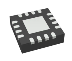
3-mm × 3-mm Thin QFN Package
APPLICATIONS
•
Active-Matrix OLED Power Supply
DESCRIPTION
The TPS65136 is designed to provide best-in-class picture quality for active-matrix OLED (AMOLED) displays
that require positive and negative supply rails. With its wide input voltage range, the device is ideally suited for
AMOLED displays, which are used in mobile phones or SmartPhone™ devices. With the new single-inductor
multiple-output (SIMO) technology, the smallest possible solution size is achieved. The device operates with a
buck-boost topology and generates both positive and negative output voltages above or below the input voltage
rail. The SIMO technology enables excellent line and load regulation. Excellent line-transient regulation is
required to avoid disturbance of the AMOLED display as a result of input voltage variations that occur during
transmit periods in mobile communication systems.
TYPICAL APPLICATION
L1
2.2 mH
TPS65136
16
15
Vin
2.3 V to 5.5 V
1
C1
10 mF
8
4
11
C4
100 nF
12
5
L1
L2
L1
L2
VIN
OUTP
EN
OUTP
VAUX
FB
PGND
FBG
PGND
OUTN
GND
OUTN
14
13
10
Vpos
4.6 V/80 mA
9
C2
4.7 mF
7
6
3
R1
464 kW
2
R2
442 kW
C3
4.7 mF
Vneg
–4.4 V/80 mA
S0337-01
1
2
3
Please be aware that an important notice concerning availability, standard warranty, and use in critical applications of Texas
Instruments semiconductor products and disclaimers thereto appears at the end of this data sheet.
SmartPhone is a trademark of Pinakin Dinesh.
All other trademarks are the property of their respective owners.
PRODUCTION DATA information is current as of publication date.
Products conform to specifications per the terms of the Texas
Instruments standard warranty. Production processing does not
necessarily include testing of all parameters.
Copyright © 2008, Texas Instruments Incorporated
�TPS65136
SLVS831A – APRIL 2008 – REVISED JULY 2008 ............................................................................................................................................................. www.ti.com
These devices have limited built-in ESD protection. The leads should be shorted together or the device placed in conductive foam
during storage or handling to prevent electrostatic damage to the MOS gates.
ORDERING INFORMATION (1)
TA
OPTIONS
–40°C to 85°C
(1)
4.6 V fixed
ORDERING P/N
PACKAGE
PACKAGE MARKING
TPS65136RTE
RTE
CCO
(2)
The RTE package is available in tape and reel. Add R suffix (TPS65136RTER) to order quantities of 3000 parts per reel. For the most
current package and ordering information, see the Package Option Addendum at the end of this document, or see the TI Web site at
www.ti.com.
Contact the factory for other output voltage options.
(2)
16-Terminal TQFN PACKAGE
OUTN
3
VAUX
4
L1
L2
L2
13
12 PGND
11 PGND
Exposed
Thermal Die
10 OUTP
9
5
6
7
8
EN
2
14
FB
OUTN
15
FBG
1
16
GND
VIN
L1
RTE Package
(Top View)
OUTP
P0081-01
TERMINAL FUNCTIONS
TERMINAL
NAME
NO.
I/O
DESCRIPTION
EN
8
I
Input pin to enable the device. Pulling this pin high enables the device. This pin has an internal 500-kΩ
pulldown resistor.
FB
7
I
Feedback regulation input for the positive output voltage rail
FBG
6
I
Feedback regulation input
GND
5
–
Analog ground
L1
13, 14
I/O
Inductor terminal
L2
15, 16
I/O
Inductor terminal
OUTN
2, 3
O
Negative output
OUTP
9, 10
O
Positive output
PGND
11, 12
–
Power GND
VAUX
4
O
Reference voltage output. This pin requires a 100-nF capacitor for stability.
VIN
1
I
Input supply
–
Connect this pad to analog GND.
Exposed thermal die
2
Submit Documentation Feedback
Copyright © 2008, Texas Instruments Incorporated
Product Folder Link(s): TPS65136
�TPS65136
www.ti.com ............................................................................................................................................................. SLVS831A – APRIL 2008 – REVISED JULY 2008
FUNCTIONAL BLOCK DIAGRAM
L1
L1
15
L2
L2
13
16
14
OVP
VIN
OUTP
VAUX
M4
1
Vpos
9
M1
OUTP
VAUX
10
M2
FB
Gate
Drive
EN
8
7
Bias (1.2 V)
UVLO
Thermal
Shutdown
FBG
6
OUTN
PGND
GND
2
5
M3
Vneg
3
VAUX
4
VAUX
Regulator
Current Limit
OUTP
+
VoltageControlled
Oscillator
VCO
OUTN
Current
Sense/
Soft Start
Ipeak
–
–
+
PWM/PFM
Control
Vref
–
+
Gate Drive
Out-of-Audio
Mode
20 kHz
OUTP
OUTP
OUTN
Short-Circuit
Protection
OUTN
11
PGND
12
PGND
B0299-01
Submit Documentation Feedback
Copyright © 2008, Texas Instruments Incorporated
Product Folder Link(s): TPS65136
3
�TPS65136
SLVS831A – APRIL 2008 – REVISED JULY 2008 ............................................................................................................................................................. www.ti.com
ABSOLUTE MAXIMUM RATINGS (1)
Over operating free-air temperature range (unless otherwise noted).
VALUE
UNIT
Input voltage range VIN (2)
–0.3 to 7
V
Voltage range at EN
–0.3 to 7
V
Voltage range at L1, OUTN
–8 to 7
V
–0.5 to 0.5
V
–0.3 to 7
V
ESD rating, HBM
2
kV
ESD rating, MM
200
V
1
kV
Voltage range at FBG
Voltage range at L2, OUTP, FB
ESD rating, CDM
Continuous total power dissipation
See Dissipation Ratings Table
TJ
Operating junction temperature range
–40 to 150
°C
TA
Operating ambient temperature range
–40 to 85
°C
Tstg
Storage temperature range
–65 to 150
°C
(1)
(2)
Stresses beyond those listed under absolute maximum ratings may cause permanent damage to the device. These are stress ratings
only, and functional operation of the device at these or any other conditions beyond those indicated under recommended operating
conditions is not implied. Exposure to absolute–maximum–rated conditions for extended periods may affect device reliability.
All voltage values are with respect to network ground terminal.
DISSIPATION RATINGS
(1)
PACKAGE
RθJA (1)
TA ≤ 25°C
POWER RATING
TA = 70°C
POWER RATING
TA = 85°C
POWER RATING
RTE
40°C/W
2.5 W
1.37 W
1W
Thermal resistance measured on a printed circuit board using thermal vias.
RECOMMENDED OPERATING CONDITIONS
MIN
TYP
MAX
UNIT
Vin
Input voltage range
2.3
5.5
V
TA
Operating ambient temperature
–40
85
°C
TJ
Operating junction temperature
–40
125
°C
ELECTRICAL CHARACTERISTICS
Vin = 3.7 V, EN = VIN, OUTP = 4.6 V, OUTN = –5.4 V, TA = –40°C to 85°C; typical values are at TA = 25°C (unless otherwise
noted).
PARAMETER
TEST CONDITIONS
MIN
TYP
MAX
UNIT
SUPPLY CURRENT
Vin
Input voltage range
IQ
Operating quiescent current into Vin
2.3
1.7
5.5
ISD
Shutdown current into Vin
0.1
VUVLO
Undervoltage lockout threshold
2
Vin falling
1.8
2
Vin rising
2
2.3
Thermal shutdown
Thermal shutdown hysteresis
V
mA
µA
V
140
°C
5
°C
ENABLE
VH
Logic high-level voltage
Vin = 2.5 V to 5.5 V
VL
Logic low-level voltage
Vin = 2.5 V to 5.5 V
R
Pulldown resistor
1.2
V
0.4
500
V
kΩ
OUTPUT
OVPP
4
Positive overvoltage protection
Iout = 10 mA
Submit Documentation Feedback
5.5
7
V
Copyright © 2008, Texas Instruments Incorporated
Product Folder Link(s): TPS65136
�TPS65136
www.ti.com ............................................................................................................................................................. SLVS831A – APRIL 2008 – REVISED JULY 2008
ELECTRICAL CHARACTERISTICS (continued)
Vin = 3.7 V, EN = VIN, OUTP = 4.6 V, OUTN = –5.4 V, TA = –40°C to 85°C; typical values are at TA = 25°C (unless otherwise
noted).
PARAMETER
Voutn
Negative output voltage range
OVPN
Negative overvoltage protection
Imis
Output current mismatch Vpos/Vneg
Voutp
Positive output voltage regulation
tdly
Sequencing delay
VFBG
Feedback ground regulation
rDS(on)
ISW
TEST CONDITIONS
MIN
TYP
–2.5
–7.6
–30%
Vpos start to Vneg start
MAX
UNIT
–6
V
–6
V
30%
4.554
4.6
4.646
6
8.7
11
ms
–10
0
10
mV
M1 MOSFET on-resistance
Isw = 100 mA
200
M2 MOSFET on-resistance
Isw = 100 mA
400
M3 MOSFET on-resistance
Isw = 100 mA
900
M4 MOSFET on-resistance
Isw = 100 mA
Switch current limit (M2)
Vin = 3.7 V
620
700
940
Vin = 2.5 V
720
830
1120
750
V
mΩ
600
mA
Pout
Output power
Vpos – Vneg ≤ 10 V; Vin = 2.9 V
fs
Switching frequency
Iout neg = Iout pos = 30 mA
1
MHz
Iout neg = Iout pos = 0 mA
40
kHz
1
V
Volow
(1)
mW
Output pulldown voltage (1)
EN = GND, Iout neg = Iout pos = 1 mA
Line regulation positive output OUTP
Iout neg = Iout pos = 5 mA
0
%/V
Line regulation negative output OUTN
Iout neg = Iout pos = 5 mA
0.008
%/V
Load regulation positive output OUTP
Vin = 3.7 V
0.27
%/A
Load regulation negative output OUTN
Vin = 3.7 V
0.25
%/A
The device actively pulls down the outputs during shutdown. The value specifies the output voltage as a current is forced into the
outputs during shutdown.
TYPICAL CHARACTERISTICS
TABLE OF GRAPHS
FIGURE
Efficiency
vs load current (2.2 µH)
Figure 1
Efficiency
vs load current (4.7 µH)
Figure 2
Operation at light load current
DCM operation
Figure 3
Operation at high load current
CCM operation
Figure 4
Line transient response
Iout = 30 mA
Figure 5
Line transient response
Iout = 50 mA
Figure 6
Start-up
Figure 7
Switching frequency
vs load current
Quiescent current
vs input voltage
Figure 8
Figure 9
Maximum output current
2.2 µH, LPS3008-222
Figure 10
Maximum output current
2.2 µH, LPF3010-2R2
Figure 11
Maximum output current
4.7 µH, LPS3008-472
Figure 12
Maximum output current
4.7 µH, LPF3010-4R7
Figure 13
Submit Documentation Feedback
Copyright © 2008, Texas Instruments Incorporated
Product Folder Link(s): TPS65136
5
�TPS65136
SLVS831A – APRIL 2008 – REVISED JULY 2008 ............................................................................................................................................................. www.ti.com
EFFICIENCY
vs
LOAD CURRENT (2.2 µH)
EFFICIENCY
vs
LOAD CURRENT (4.7 µH)
80
80
70
70
60
50
50
Efficiency − %
Efficiency − %
VI = 4.5 V
60
VI = 2.5 V
40
VI = 3.7 V
30
20
30
VI = 4.5 V
L = 2.2 µH
Vpos = 4.6 V
Vneg = −5 V
1
10
100
L = 4.7 µH
Vpos = 4.6 V
Vneg = −5 V
10
1k
IO − Load Current − mA
6
VI = 3.7 V
40
20
10
0
0.1
VI = 2.5 V
0
0.1
G001
1
10
100
IO − Load Current − mA
Figure 1.
Figure 2.
OPERATION AT LIGHT LOAD CURRENT
DCM OPERATION
OPERATION AT HIGH LOAD CURRENT
CCM OPERATION
Figure 3.
Figure 4.
Submit Documentation Feedback
1k
G002
Copyright © 2008, Texas Instruments Incorporated
Product Folder Link(s): TPS65136
�TPS65136
www.ti.com ............................................................................................................................................................. SLVS831A – APRIL 2008 – REVISED JULY 2008
LINE TRANSIENT RESPONSE
Iout = 30 mA
LINE TRANSIENT RESPONSE
Iout = 50 mA
Figure 5.
Figure 6.
START-UP
SWITCHING FREQUENCY
vs
LOAD CURRENT
3000
f − Switching Frequency − kHz
2500
VI = 4.5 V
2000
VI = 3.7 V
1500
VI = 2.5 V
1000
500
0
0
20
40
60
80
100
IO − Load Current − mA
Figure 7.
120
G008
Figure 8.
Submit Documentation Feedback
Copyright © 2008, Texas Instruments Incorporated
Product Folder Link(s): TPS65136
7
�TPS65136
SLVS831A – APRIL 2008 – REVISED JULY 2008 ............................................................................................................................................................. www.ti.com
QUIESCENT CURRENT
vs
INPUT VOLTAGE
MAXIMUM OUTPUT CURRENT
2.2 µH, LPS3008-222
5.0
10.2
L = 2.2 µH
VO = Vpos + |Vneg| = 10 V
TA = 85°C
4.5
10.1
3.5
VO − Output Voltage − V
Iq − Quiescent Current − mA
4.0
TA = 85°C
3.0
2.5
TA = 25°C
2.0
1.5
VI = 2.5 V
10.0
VI = 2.9 V
VI = 2.3 V
9.9
1.0
TA = −40°C
0.5
0.0
2.0
9.8
2.5
3.0
3.5
4.0
4.5
5.0
5.5
VI − Input Voltage − V
6.0
30
60
70
80
90
G009
100
G010
Figure 9.
Figure 10.
MAXIMUM OUTPUT CURRENT
2.2 µH, LPF3010-2R2
MAXIMUM OUTPUT CURRENT
4.7 µH, LPS3008-472
10.2
L = 4.7 µH
VO = Vpos + |Vneg| = 10 V
TA = 85°C
L = 2.2 µH
VO = Vpos + |Vneg| = 10 V
TA = 85°C
10.1
VO − Output Voltage − V
10.1
VI = 2.9 V
10.0
VI = 2.3 V
9.9
VI = 2.9 V
10.0
VI = 2.3 V
9.9
VI = 2.5 V
VI = 2.5 V
9.8
9.8
30
40
50
60
70
80
IO − Output Current − mA
90
100
30
G011
Figure 11.
8
50
IO − Output Current − mA
10.2
VO − Output Voltage − V
40
40
50
60
70
80
IO − Output Current − mA
90
100
G012
Figure 12.
Submit Documentation Feedback
Copyright © 2008, Texas Instruments Incorporated
Product Folder Link(s): TPS65136
�TPS65136
www.ti.com ............................................................................................................................................................. SLVS831A – APRIL 2008 – REVISED JULY 2008
MAXIMUM OUTPUT CURRENT
4.7 µH, LPF3010-4R7
10.2
L = 4.7 µH
VO = Vpos + |Vneg| = 10 V
TA = 85°C
VO − Output Voltage − V
10.1
VI = 2.9 V
10.0
VI = 2.3 V
9.9
VI = 2.5 V
9.8
30
40
50
60
70
80
IO − Output Current − mA
90
100
G013
Figure 13.
DETAILED DESCRIPTION
The TPS65136 operates with a four-switch buck-boost converter topology, generating a negative and a positive
output voltage with a single inductor. The device uses the SIMO regulator technology featuring best-in-class
line-transient regulation, buck-boost mode for the positive and negative outputs, and highest efficiency over the
entire load-current range. High efficiency over the entire load-current range is implemented by reducing the
converter switching frequency. Out-of-audio mode avoids the switching frequency going below 20 kHz.
As illustrated in the functional block diagram, the converter operates with two control loops. One error amplifier
sets the output voltage for the positive output, OUTP. The ground error amplifier regulates FBG to typically 0 V.
Using the external feedback divider allows setting the output voltage of the negative output, OUTN. In principle,
the converter topology operates just like any other buck-boost converter topology with the difference that the
output voltage across the inductor is the sum of the positive and negative output voltages. With this
consideration, all calculations of the buck-boost converter apply for this topology as well. During the first switch
cycle, M1 and M2 are closed, connecting the inductor from VIN to GND. During the second switch cycle, the
inductor discharges to the positive and negative outputs by closing switches M4 and M3. Because the inductor is
discharged to both of the outputs simultaneously, the output voltages can be higher or lower than the input
voltage. In addition to that, the converter operates best when the current out of OUTP is equal to the current
flowing into OUTN. This is usually the case when driving an AMOLED panel. Any asymmetries in load current
can be canceled out by the ground error amplifier connected to FBG. However, this is only possible for current
asymmetries of typically 30%. During light load current in discontinuous conduction mode, the converter operates
in peak-current-mode control with the switching cycle given by the internal voltage-controlled oscillator (VCO). As
the load current increases, the converter operates in continuous-conduction mode. In this mode, the converter
moves to peak-current control with the switch cycle given by the fixed off-time. The SIMO regulator topology has
excellent line transient regulation when operating in discontinuous conduction mode. As the load current
increases, entering continuous conduction mode, the line transient performance is linearly decreased.
Submit Documentation Feedback
Copyright © 2008, Texas Instruments Incorporated
Product Folder Link(s): TPS65136
9
�TPS65136
SLVS831A – APRIL 2008 – REVISED JULY 2008 ............................................................................................................................................................. www.ti.com
Advanced Power-Save Mode for Light-Load Efficiency
In order to maintain high efficiency over the entire load-current range, the converter reduces its switching
frequency as the load current decreases. The advanced power-save mode controls the switching frequency
using a voltage-controlled oscillator (VCO). The VCO frequency is proportional to the inductor peak current, with
a lower frequency limit of 20 kHz. This avoids disturbance of the audio band and minimizes audible noise coming
from the ceramic input and output capacitors. By maintaining a controlled switching frequency, possible EMI is
minimized. This is especially important when using the device in mobile phones. See Figure 8 for typical
switching frequency versus load current.
Buck-Boost Mode Operation
Buck-boost mode operation allows the input voltage to be higher than the output voltage. This mode allows the
use of batteries and supply voltages that are above the fixed 4.6-V output voltage of OUTP.
Inherent Excellent Line-Transient Regulation
The SIMO regulator achieves inherent superior line-transient regulation when operating in discontinuous
conduction mode, shown in Figure 5 and Figure 6. In discontinuous conduction mode, the current delivered to
the output is given by the inductor peak current and falling slope of the inductor current. This is shown in
Figure 14, where the output current, given by the area A, is the same for different input voltages. Because the
converter uses peak-current-mode control, the peak current is fixed as long as the load current is fixed. The
falling slope of the inductor current is given by the sum of the output voltage and inductor value. This is also a
fixed value and independent of the input voltage. Because of this, any change in input voltage changes the
converter duty cycle but does not change the inductor peak current or the falling slope of the inductor current.
Therefore, the output current, given by the area A (Figure 14), remains constant over any input voltage variation.
Because the area A is constant, the converter has an inherently perfect line regulation when operating in
discontinuous conduction mode. Entering continuous conduction mode (CCM) linearly decreases the
line-transient performance. However, the line-transient response in CCM is still as good as for any standard
current-mode-controlled switching converter. The following formulas detail the relations of the TPS65136
converter topology operating in CCM.
Vpos + Vneg
Vin
L
Ip
L
A
A
tclock
M0116-01
Figure 14. Inherently Perfect Line-Transient Regulation
The converter always sees the sum of the negative and positive output voltage, which is calculated as:
Vo = Voutp + Voutn
The converter duty cycle is calculated using the efficiency estimation from the data sheet curves or from real
application measurements. A 70% efficiency value is a good value to go through the calculations.
Vo
D=
Vin g h + Vo
The output current for entering continuous conduction mode can be calculated. The switching frequency can be
obtained from the data sheet graphs. A frequency of 1.5 MHz is usually sufficient for these types of calculations.
10
Submit Documentation Feedback
Copyright © 2008, Texas Instruments Incorporated
Product Folder Link(s): TPS65136
�TPS65136
www.ti.com ............................................................................................................................................................. SLVS831A – APRIL 2008 – REVISED JULY 2008
Ic =
Vo g (1 - D)2
fS g 2 g L
(1)
The inductor ripple current when operating in CCM can also be calculated.
V gD
DiL = in
L g fS
Last but not least, the converter switch peak current is calculated.
I
V gD
Isw = in
+ out
2 g f g L 1- D
(2)
Overvoltage Protection
The device monitors both the positive and negative output voltages. The positive regulator monitors the positive
output and reduces the current limit when the output voltage exceeds the overvoltage protection limit. The
negative output is clamped using a zener diode, typically to –7.6 V.
Short-Circuit Protection
Both outputs are protected against short circuits either to GND or against the other output. For the positive
output, the device switching frequency and the current limit are reduced in case of a short circuit.
Soft-Start Operation
The device increases the current limit during soft-start operation to avoid high inrush currents during start-up.
The current limit typically ramps up to its full-current limit within 100 µs.
Start-Up Sequencing
The TPS65136 includes an internal, fixed start-up sequence, where the negative output voltage rail comes up
after the positive output voltage rail. The device starts the positive rail first, and an internal counter delays the
start-up of the negative rail, typically by 8.7 ms. The negative rail is clamped, typically to –0.4 V, until the internal
timer commands the negative rail to start up.
Vpos
8.7 ms
Vneg
T0298-01
Figure 15. Start-Up Sequencing
Output-Current Mismatch
The device operates best when the current of the positive output is similar to the current of the negative output.
However, the device is able to regulate an output-current mismatch between the outputs of up to 30%. If the
output-current mismatch becomes much larger, then one of the outputs goes out of regulation.
Input Capacitor Selection
The device typically requires a 10-µF ceramic input capacitor. Larger values can be used to lower the input
voltage ripple. Table 1 lists capacitors suitable for use on the TPS65136 input.
Submit Documentation Feedback
Copyright © 2008, Texas Instruments Incorporated
Product Folder Link(s): TPS65136
11
�TPS65136
SLVS831A – APRIL 2008 – REVISED JULY 2008 ............................................................................................................................................................. www.ti.com
Table 1. Input Capacitor Selection
CAPACITOR
COMPONENT SUPPLIER
SIZE
10 µF/10 V
Taiyo Yuden LMK212BJ106
0805
10 µF/6.3 V
Taiyo Yuden JMK107BJ106
0603
Inductor Selection/Efficiency/Line-Transient Response
The device is internally compensated and provides stable operation with either a 4.7-µH or 2.2-µH inductor. For
this type of converter, the inductor selection is a key element in the design process, because it has an impact on
several application parameters. The inductor selection influences the converter efficiency, line transient
response, and maximum output current. Because the inductor ripple current is fairly large in this type of
application, the inductor has a major impact on the overall converter efficiency. Having large inductor ripple
current causes the inductor core and magnetizing losses to become dominant. Due to this, an inductor with a
larger dc winding resistance can possibly achieve higher converter efficiencies when having lower core and
magnetizing losses. Therefore, minimizing inductor ripple current also increases the overall converter efficiency.
A 4.7-µH inductor achieves a higher efficiency compared to a 2.2-µH inductor, due to lower inductor ripple
current. The inductor value also influences the line transient regulation. This is because the inductor value
influences the current range entering continuous conduction mode (CCM). As discussed, the line transient
performance decreases when entering CCM. The larger the inductor value, the lower the load current when
entering CCM. The formula to calculate the current entering CCM is shown in Equation 1. The inductors listed in
Table 2 achieve a good overall converter efficiency while having a low device profile of just 0,8 mm. The inductor
saturation current should be 900 mA, depending on the maximum output current of the application. See
Equation 2, where the converter switch current limit is calculated. The converter switch current is equal to the
peak inductor current.
Table 2. Inductor Selection
INDUCTOR VALUE
COMPONENT SUPPLIER
DIMENSIONS in mm
Isat/DCR
2.2 µH
Coilcraft LPS3008-222
2,95 × 2,95 × 0,8
1.1 A/175 mΩ
2.2 µH
TOKO FDSE0312-2R2
3,3 × 3,3 × 1,2
1.2 A/160 mΩ
2.2 µH
ABCO LPF3010T-2R2
2,8 × 2,8 × 1
1.0A/100 mΩ
2.2 µH
Maruwa CXFU0208-2R2
2,65 × 2,65 × 0,8
0.85A/185 mΩ
4.7 µH
Maruwa CXFU0208-4R7
2,65 × 2,65 × 0,8
0.51A/440 mΩ
4.7 µH
Coilcraft LPS3008-472
2,95 × 2,95 × 0,8
0.8 A/350 mΩ
4.7 µH
ABCO LPF3010T-4R7
2,8 × 2,8 × 1
0.7A/280 mΩ
Output Capacitor Selection
A 4.7-µF output capacitor is generally sufficient for most applications, but larger values can be used as well for
improved line-transient response at higher load currents. The capacitor of Table 3 is recommended for use with
the TPS65136.
Table 3. Output Capacitor Selection
CAPACITOR
COMPONENT SUPPLIER
SIZE
4.7 µF/10V
Taiyo Yuden LMK107BJ475
0603
Setting the Negative Output Voltage OUTN
For highest output-voltage accuracy, the TPS65136 has an internally fixed output voltage for the positive output.
The negative output voltage is adjustable. Because the feedback FBG is regulated to ground, the voltage across
R1 is equal to the positive output voltage of 4.6 V. R1 is selected to have at least 10 µA through the feedback
divider.
4.6 V
R1 =
» 464 kW
10 μA
R2 is then calculated as:
12
Submit Documentation Feedback
Copyright © 2008, Texas Instruments Incorporated
Product Folder Link(s): TPS65136
�TPS65136
www.ti.com ............................................................................................................................................................. SLVS831A – APRIL 2008 – REVISED JULY 2008
R2 =
Vneg
4.6 V
´ R1
PCB Layout Guidelines
PCB layout is an important task in the power supply design. Good PCB layout minimizes EMI and allows very
good output voltage regulation. For the TPS65136, the following PCB layout guidelines are recommended.
Place the power components first. The inductor and the input and output capacitors must be as close as possible
to the IC pins. Place the bypass capacitor for the reference output voltage VAUX as close as possible to pin 4.
Use bold and wide traces for power traces connecting the inductor and input and output capacitors. Use a
common ground plane or a start ground connection.
See the TPS65136EVM-063 user's guide (SLVU244) and evaluation module for a PCB layout example.
Submit Documentation Feedback
Copyright © 2008, Texas Instruments Incorporated
Product Folder Link(s): TPS65136
13
�TPS65136
SLVS831A – APRIL 2008 – REVISED JULY 2008 ............................................................................................................................................................. www.ti.com
TYPICAL APPLICATION
L1
2.2 mH
TPS65136
16
15
Vin
2.3 V to 5.5 V
1
C1
10 mF
8
4
11
C4
100 nF
12
5
L1
L2
L1
L2
VIN
OUTP
EN
OUTP
VAUX
FB
PGND
FBG
PGND
OUTN
GND
OUTN
14
13
10
Vpos
4.6 V/80 mA
9
C2
4.7 mF
7
6
3
R1
464 kW
2
R2
442 kW
C3
4.7 mF
Vneg
–4.4 V/80 mA
S0337-01
Figure 16. Standard Application AMOLED Supply
14
Submit Documentation Feedback
Copyright © 2008, Texas Instruments Incorporated
Product Folder Link(s): TPS65136
�PACKAGE OPTION ADDENDUM
www.ti.com
6-Feb-2020
PACKAGING INFORMATION
Orderable Device
Status
(1)
Package Type Package Pins Package
Drawing
Qty
Eco Plan
Lead/Ball Finish
MSL Peak Temp
(2)
(6)
(3)
Op Temp (°C)
Device Marking
(4/5)
TPS65136RTER
ACTIVE
WQFN
RTE
16
3000
Green (RoHS
& no Sb/Br)
NIPDAU
Level-2-260C-1 YEAR
-40 to 85
CCO
TPS65136RTERG4
ACTIVE
WQFN
RTE
16
3000
Green (RoHS
& no Sb/Br)
NIPDAU
Level-2-260C-1 YEAR
-40 to 85
CCO
(1)
The marketing status values are defined as follows:
ACTIVE: Product device recommended for new designs.
LIFEBUY: TI has announced that the device will be discontinued, and a lifetime-buy period is in effect.
NRND: Not recommended for new designs. Device is in production to support existing customers, but TI does not recommend using this part in a new design.
PREVIEW: Device has been announced but is not in production. Samples may or may not be available.
OBSOLETE: TI has discontinued the production of the device.
(2)
RoHS: TI defines "RoHS" to mean semiconductor products that are compliant with the current EU RoHS requirements for all 10 RoHS substances, including the requirement that RoHS substance
do not exceed 0.1% by weight in homogeneous materials. Where designed to be soldered at high temperatures, "RoHS" products are suitable for use in specified lead-free processes. TI may
reference these types of products as "Pb-Free".
RoHS Exempt: TI defines "RoHS Exempt" to mean products that contain lead but are compliant with EU RoHS pursuant to a specific EU RoHS exemption.
Green: TI defines "Green" to mean the content of Chlorine (Cl) and Bromine (Br) based flame retardants meet JS709B low halogen requirements of