TPS65170
www.ti.com
SLVSA27 – OCTOBER 2009
LCD Bias Supply
Check for Samples :TPS65170
FEATURES
1
•
•
•
•
•
•
•
•
•
•
•
•
•
8.6V to 14.7V Input Voltage Range
2.8A Boost Converter Switch Current Limit
Boost Converter Output Voltages up to 18.5V
Boost and Buck Converter Short-Circuit
Protection
1.5A Buck Converter Switch Current Limit
Fixed 750kHz Switching Frequency for Buck
and Boost Converters
Fixed Buck Converter Soft-Start
Programmable Boost Converter Soft-Start
Two Charge Pump Controllers to Regulate VGH
and VGL
Control Signal for External High-Side MOSFET
Isolation Switch
Reset Signal With Programmable Reset Pulse
Duration
Thermal Shutdown
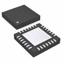
28-Pin 5×5 mm QFN Package
APPLICATIONS
•
LCD TVs and Monitors
DESCRIPTION
The TPS65170 also provides a reset circuit that
monitors the buck converter output (VLOGIC) and
generates a reset signal for the timing controller
during power-up.
A control signal can also be generated to control an
external MOSFET isolation switch located between
the output of the boost converter and the display
panel.
Isolation Switch
Control
Boost
Converter
Buck
Converter
Positive
LDO Controller
Negative
LDO Controller
Reset
Generator
The TPS65170 provides a simple and economic
power supply solution for a wide variety of LCD bias
applications.
In typical display panel applications, the boost
converter generates the display panel’s source
voltage VS, the buck converter generates the
system’s logic supply VLOGIC, and the two charge
pump controllers regulate the external charge pumps
generating the display transistors’ on and off supplies
VGH and VGL.
By using external transistors to regulate the charge
pump output voltage, power dissipation in the IC is
significantly reduced, simplifying PCB thermal design
and improving reliability.
1
Please be aware that an important notice concerning availability, standard warranty, and use in critical applications of Texas
Instruments semiconductor products and disclaimers thereto appears at the end of this data sheet.
PRODUCTION DATA information is current as of publication date.
Products conform to specifications per the terms of the Texas
Instruments standard warranty. Production processing does not
necessarily include testing of all parameters.
Copyright © 2009, Texas Instruments Incorporated
�TPS65170
SLVSA27 – OCTOBER 2009
www.ti.com
This integrated circuit can be damaged by ESD. Texas Instruments recommends that all integrated circuits be handled with
appropriate precautions. Failure to observe proper handling and installation procedures can cause damage.
ESD damage can range from subtle performance degradation to complete device failure. Precision integrated circuits may be more
susceptible to damage because very small parametric changes could cause the device not to meet its published specifications.
ORDERING INFORMATION (1)
(1)
TA
ORDERING
PACKAGE
–40°C to 85°C
TPS65170RHDR
28-Pin 5x5 QFN
The device is supplied taped and reeled, with 3000 devices per reel.
ABSOLUTE MAXIMUM RATINGS
over operating free-air temperature range (unless otherwise noted)
(1)
VALUE
UNIT
Input voltage (2)
VIN
-0.3 to 20
V
Input voltage (2)
FBN, FBP, FBB, FB, DLY, CRST, SS, COMP, VL
-0.3 to 7
V
RST
-0.3 to 7
V
SWB, CTRLP, GD, SW, CTRLN
-0.3 to 20
V
1
mA
Human Body Model
2000
V
Machine Model
200
V
Charged Device Model
700
V
See Dissipation Table
W
Operating ambient temperature range
–40 to 85
°C
Operating junction temperature range
–40 to 150
°C
Storage temperature range
–65 to 150
°C
Output voltage (2)
Output current
ESD rating
GD
Continuous Power Dissipation
(1)
(2)
Stresses beyond those listed under absolute maximum ratings may cause permanent damage to the device. These are stress ratings
only and functional operation of the device at these or any other conditions beyond those indicated under recommended operating
conditions is not implied. Exposure to absolute-maximum-rated conditions for extended periods may affect device reliability.
With respect to the GND and AGND pins.
DISSIPATION RATINGS
PACKAGE
θJA
TA ≤ 25°C
POWER RATING
TA = 70°C
POWER RATING
TA = 85°C
POWER RATING
28-Pin QFN
34 °C/W
2.94 W
1.62 W
1.32 W
RECOMMENDED OPERATING CONDITIONS
over operating free-air temperature range (unless otherwise noted)
MIN
TYP
MAX
UNIT
V
VIN
Input voltage range
VS
Boost converter output voltage range
LBOOST
Boost converter inductance
CBOOST
LBUCK
CBUCK
Buck converter output capacitance
TA
Operating ambient temperature
TJ
Operating junction temperature
–40
2
8.6
12
14.7
VIN+1
15
18.5
6.8
10
15
Boost converter output capacitance
50
60
100
µF
Buck converter inductance
6.8
10
15
µH
20
44
100
µF
–40
25
85
°C
85
125
°C
Submit Documentation Feedback
V
µH
Copyright © 2009, Texas Instruments Incorporated
Product Folder Link(s) :TPS65170
�TPS65170
www.ti.com
SLVSA27 – OCTOBER 2009
ELECTRICAL CHARACTERISTICS
VIN = 12V; VS = 17V; VLOGIC = 3.3V; TA = –40°C to 85°C; typical values are at 25°C (unless otherwise noted)
PARAMETER
TEST CONDITIONS
MIN
TYP
MAX
UNIT
1
10
mA
7.8
8.2
8.5
V
600
750
900
kHz
18.5
V
1%
V
±0.01
±1
µA
3.5
4.2
A
10
µA
POWER SUPPLY
IIN
Supply current
VFB, VFBB, VFBP = 1.3V, VFBN = –50mV
UVLO
UVLO threshold
VIN rising
INTERNAL OSCILLATOR
fSW
Switching frequency
BOOST CONVERTER
VS
Output voltage
VFB
Feedback regulation voltage
Measured after isolation switch
IFB
Feedback input bias current
ILIM
Switch current limit
Ilkg
Switch leakage current
VSW = 12V
rDS(on)
Switch ON resistance
ISW = ILIM
tSW
Switching time
Turn-on and turn-off
Line regulation
9.6V < VIN < 14.4V, IS = 750mA
Load regulation
VS = 17V, IS = 100mA to 1.5A
VOVP
Overvoltage threshold
VFB rising
ISS
Soft start current
VSS = 1.24V
VFB(SC)
Short circuit threshold
VFB rising
13
–1%
VFB = 1.24V
2.8
1.24
0.12
0.22
10
Ω
ns
0.02
%/V
0.1
%/A
VFB +3%
VFB +5%
V
10
µA
200
mV
BUCK CONVERTER
VLOGIC
Output voltage
IFBB
Feedback input bias current
–3%
3.3
ILIM
Switch current limit
Ilkg
Switch leakage current
rDS(on)
Switch ON resistance
tSW
Switching time
Turn-on and turn-off
Line regulation
VIN = 9.6V to 14.4V, ILOGIC = 0.5A
0.01
%/V
Load regulation
ILOGIC = 150mA to 1.5A
0.2
%/A
VPG
Power good threshold
VLOGIC rising
3.2
V
VFBB(SC)
Short circuit threshold
VFBB rising
tSS
Soft start time
VFBB = 3.3V
1.5
2.1
VSWB = GND
0.21
3%
V
±125
µA
2.8
A
10
µA
0.35
10
Ω
ns
1.065
V
0.66
ms
POSITIVE CHARGE PUMP CONTROLLER
VFBP
Feedback regulation voltage
ICTRLP = 1mA (sinking)
IFBP
Feedback input bias current
VFBP = 1.24V
ICTRLP
Base drive current for external
transistor
Normal operation (sinking)
Line regulation
VIN = 9.6V to 14.4V, VGH = 27V, IGH =
50mA, including external components
Load regulation
VGH = 27V, IGH = 10mA to 50mA,
including external components
Short-circuit operation (sinking)
-3%
1.24
+3%
V
±1
±100
nA
55
75
5
40
mA
µA
±0.1
%/V
±1
%/A
NEGATIVE CHARGE PUMP CONTROLLER
VFBN
Feedback regulation voltage
ICTRLN = 1mA (sourcing)
IFBN
Feedback input bias current
VFBN = 0V
–36
ICTRLN
Base drive current for external
transistor
Normal operation (sourcing)
2.5
Short-circuit operation (sourcing)
200
Line regulation
VIN = 9.6V to 14.4V, VGL = -7V, IGL =
50mA, including external components
0
36
mV
±1
±100
nA
300
480
mA
±0.1
Submit Documentation Feedback
Copyright © 2009, Texas Instruments Incorporated
Product Folder Link(s) :TPS65170
µA
%/V
3
�TPS65170
SLVSA27 – OCTOBER 2009
www.ti.com
ELECTRICAL CHARACTERISTICS (continued)
VIN = 12V; VS = 17V; VLOGIC = 3.3V; TA = –40°C to 85°C; typical values are at 25°C (unless otherwise noted)
PARAMETER
TEST CONDITIONS
Load regulation
MIN
VGL = –7V, IGH = 10mA to 50mA,
including external components
TYP
MAX
±1
UNIT
%/A
RESET GENERATOR
VRST
Output voltage low
IRST 1mA (sinking)
IRST
Output current high
VRST = 3.3V (sinking)
ICRST
Reset delay capacitor charge
current
VCRST = 1.24V
VCRST
Reset delay threshold voltage
VCRST rising
0.5
V
1
µA
10
µA
1.24
V
ISOLATION SWITCH CONTROL
VGD
Output voltage low
IGD = 500µA (sinking)
ILKG
Leakage Current
VGD = 20V
IDLY
Delay capacitor charge current
VDLY = 1.24V
VDLY
Delay threshold voltage
VDLY rising
0.05
0.5
V
1
µA
DELAY DLY
10
µA
1.24
V
THERMAL SHUTDOWN
TSD
Thermal shutdown threshold
150
°C
THYS
Thermal shutdown hysteresis
10
°C
DEVICE INFORMATION
PIN ASSIGNMENT
4
VIN
VIN
PGND
PGND
SW
SW
GD
28
27
26
25
24
23
22
Top View
VL
1
21 CTRLP
SWB
2
20 FBP
SWB
3
19 FB
Exposed
Thermal Die
16 CRST
RST
7
15 DLY
AGND 14
18 COMP
NC 13
NC 12
6
NC 11
FBB
NC 10
17 SS
9
5
NC
FBN
8
4
AGND
CTRLN
Submit Documentation Feedback
Copyright © 2009, Texas Instruments Incorporated
Product Folder Link(s) :TPS65170
�TPS65170
www.ti.com
SLVSA27 – OCTOBER 2009
PIN FUNCTIONS
PIN
NAME
VL
NO.
I/O
DESCRIPTION
1
O
Connection for decoupling capacitor for internal bias supply.
2, 3
O
Buck converter switch node
CTRLN
4
O
Base drive signal for the positive charge pump external regulating transistor.
FBN
5
I
Feedback pin for the negative charge pump. Connect this pin to the center of a resistor divider
connected between the negative charge pump output and buck converter output.
FBB
6
I
Buck converter feedback. Connect this pin to the output of the buck converter.
/RST
7
O
Reset generator open drain output
AGND
8
P
Analog ground
9, 10, 11,
12, 13
N/A
AGND
14
P
Analog ground.
DLY
15
I
Positive charge pump and boost converter delay capacitor connection.
CRST
16
I
Reset generator timing capacitor connection.
SS
17
I
Soft-start timing capacitor connection.
COMP
18
I
Boost converter compensation network connection.
FB
19
I
Boost regulator feedback. Connect this pin to the center of a resistor divider connected between the
boost converter output and AGND.
FBP
20
I
Feedback pin for the positive charge pump. Connect this pin to the center of a resistor divider
connected between the positive charge pump output and AGND.
CTRLP
21
O
Base drive signal for the positive charge pump external regulating transistor
GD
22
O
Gate drive signal for the external MOSFET isolation switch.
SW
23, 24
O
Boost converter switching node
PGND
25, 26
P
Power ground
VIN
27, 28
P
Supply voltage connection
P
Connect to the system GND
SWB
NC
Exposed
Thermal Die
Not used, connect to AGND.
Submit Documentation Feedback
Copyright © 2009, Texas Instruments Incorporated
Product Folder Link(s) :TPS65170
5
�TPS65170
SLVSA27 – OCTOBER 2009
www.ti.com
TYPICAL CHARACTERISTICS
TABLE OF GRAPHS
FIGURE NO.
BOOST CONVERTER
Efficiency
VIN = 12 V, VS = 15.5V
Figure 1
Load Transient Response
VIN = 12 V, VS = 15.5V, IS = 250 mA to 750 mA
Figure 2
Line Transient Response
VIN = 11.5 V to 12.5 V, VS = 15.5 V, IS = 750 mA, VGH = 26V, IGH = 50 mA
Figure 3
Output Voltage Ripple
VIN = 12 V, VS = 15.5 V, IS = 500 mA, VGH = 26V, IGH = 50 mA
Figure 4
CCM Operation, VIN = 12 V, IS = 250 mA
Figure 5
DCM Operation, VIN = 12 V, IS = 50 mA
Figure 6
Efficiency
VIN = 12 V, VLOGIC = 3.3V
Figure 7
Load Transient Response
VIN = 12 V, VGL = -7V, IGL = 50mA, ILOGIC = 250 mA to 500 mA
Figure 8
Line Transient Response
VIN = 11.5 V to 12.5 V, VGL = -7V, IGL = 50mA, ILOGIC = 500 mA
Figure 9
Output Voltage Ripple
VIN = 12 V, VGL = -7V, IGL = 50mA, ILOGIC = 500 mA
Figure 10
CCM Operation, VIN = 12 V, ILOGIC = 250 mA
Figure 11
DCM Operation, VIN = 12 V, ILOGIC = 50 mA
Figure 12
Skip Mode, VIN = 12 V, ILOGIC = 0 mA
Figure 13
Load Transient Response
VIN = 12 V, VGH = 26 V, VS = 15.5V, IS = 250 mA, IGH = 10 mA to 50 mA
Figure 14
Line Transient Response
VIN = 11.5 V to 12.5 V, VGH = 26 V, IGH = 50 mA, VS = 15.5V, IS = 750
mA,
Figure 15
Output Voltage Ripple
VIN = 12 V, VGH = 26 V, IGH = 50 mA, VS = 15.5V, IS = 750 mA,
Figure 16
Load Transient Response
VIN = 12 V, VGL = -7 V, ILOGIC = 250 mA, IGL = 10 mA to 50 mA
Figure 17
Line Transient Response
VIN = 11.5 V to 12.5 V, VGL = -7 V, IGL = 50 mA, ILOGIC = 250 mA
Figure 18
Output Voltage Ripple
VIN = 12 V, VGL = -7 V, ILOGIC = 250 mA, IGL = 50 mA
Figure 19
Switch Node (SW) Waveform
BUCK CONVERTER
Switch Node (SW) Waveform
POSITIVE CHARGE PUMP
NEGATIVE CHARGE PUMP
START-UP SEQUENCING
Power-Up Sequencing
Figure 20
Reset Operation
Figure 21
BOOST CONVERTER LOAD TRANSIENT RESPONSE
IS = 250 mA to 750 mA
BOOST CONVERTER EFFICIENCY
vs OUTPUT CURRENT
100
90
VIN = 12 V
VS = 15.5 V
80
Efficiency - %
70
VS
60
50
40
30
IS
20
VIN = 12 V,
VS = 15.5 V
10
0
0
0.25
0.5
0.75
1
IO - Output Current - A
1.25
1.5
Figure 1.
6
Figure 2.
Submit Documentation Feedback
Copyright © 2009, Texas Instruments Incorporated
Product Folder Link(s) :TPS65170
�TPS65170
www.ti.com
SLVSA27 – OCTOBER 2009
BOOST CONVERTER LINE TRANSIENT RESPONSE
VIN = 11.5 V to 12.5 V
BOOST CONVERTER OUTPUT VOLTAGE RIPPLE
IS = 500 mA
VIN = 12 V,
VS = 15.5 V,
VGH = 26 V,
IGH = 50 mA
VS = 15.5 V,
IS = 750 mA,
VGH = 26 V,
IGH = 50 mA
VS
VS
VIN
Figure 3.
Figure 4.
BOOST CONVERTER SWITCH NODE WAVEFORM
CONTINUOUS CONDUCTION MODE
BOOST CONVERTER SWITCH NODE WAVEFORM
DISCONTINUOUS CONDUCTION MODE
VSW
VSW
IINDUCTOR
IINDUCTOR
VIN = 12 V,
Is = 50 mA
VIN = 12 V,
IS = 250 mA
Figure 5.
Figure 6.
BUCK CONVERTER LOAD TRANSIENT RESPONSE
ILOGIC = 250 mA to 500 mA
BUCK CONVERTER EFFICIENCY
vs OUTPUT CURRENT
100
VIN = 12 V,
VLOGIC = 3.3 V
90
VIN = 12 V,
VGH = -7 V,
IGH = 50 mA
80
Efficiency - %
70
VLOGIC
60
50
ILOGIC
40
30
20
10
0
0
0.25
0.5
0.75
1
IO - Output Current - A
1.25
1.5
Figure 7.
Figure 8.
Submit Documentation Feedback
Copyright © 2009, Texas Instruments Incorporated
Product Folder Link(s) :TPS65170
7
�TPS65170
SLVSA27 – OCTOBER 2009
www.ti.com
BUCK CONVERTER LINE TRANSIENT RESPONSE
VIN = 11.5 V to 12.5 V
BUCK CONVERTER OUTPUT VOLTAGE RIPPLE
ILOGIC = 500 mA
VIN = 12 V,
VGH = -7 V,
IGH = 50 mA
Ilogic = 500 mA,
VGH = -7 V,
IGH = 50 mA
VLOGIC
VLOGIC
ILOGIC
Figure 9.
Figure 10.
BUCK CONVERTER SWITCH NODE WAVEFORM
CONTINUOUS CONDUCTION MODE
BUCK CONVERTER SWITCH NODE WAVEFORM
DISCONTINUOUS CONDUCTION MODE
VSWB
VSWB
IINDUCTOR
IINDUCTOR
VIN = 12 V,
ILOGIC = 250 mA
VIN = 12 V,
ILOGIC = 50 mA
Figure 11.
Figure 12.
BUCK CONVERTER SWITCH WAVEFORM
SKIP MODE
POSITIVE CHARGE PUMP LOAD TRANSIENT RESPONSE
IGH = 10 mA to 50 mA
VGH
VSWB
VIN = 12 V,
VGH = 26 V,
VS = 15.5 V,
IS = 250 mA
IGH
IINDUCTOR
VIN = 12 V,
ILOGIC = 0 mA
Figure 13.
8
Figure 14.
Submit Documentation Feedback
Copyright © 2009, Texas Instruments Incorporated
Product Folder Link(s) :TPS65170
�TPS65170
www.ti.com
SLVSA27 – OCTOBER 2009
POSITIVE CHARGE PUMP LINE TRANSIENT RESPONSE
VIN = 11.5 V to 12.5 V
POSITIVE CHARGE PUMP OUTPUT VOLTAGE RIPPLE
IGH = 50 mA
VGH = 26 V,
IGH = 50 mA,
VS = 15.5 V,
IS = 750 mA
VGH
VGH
IGH
VIN = 12 V,
VGH = 26 V,
VS = 15.5 V,
IS = 750 mA
Figure 15.
Figure 16.
NEGATIVE CHARGE PUMP LOAD TRANSIENT RESPONSE
IGL = 10 mA to 50 mA
NEGATIVE CHARGE PUMP LINE TRANSIENT RESPONSE
VIN = 11.5 V to 12.5 V
VIN = 12 V,
VGH = -7 V,
ILOGIC = 250 mA
VGL = -7 V,
IGL = 50 mA,
ILOGIC = 250 mA
VGL
VGL
IGL
IGL
Figure 17.
Figure 18.
NEGATIVE CHARGE PUMP OUTPUT VOLTAGE RIPPLE
IGL = 50mA
POWER-UP SEQUENCING
VLOGIC
VIN = 12 V,
VGL = -7 V,
ILOGIC = 250 mA
VGL
VGL
VS
VGH
Figure 19.
Figure 20.
Submit Documentation Feedback
Copyright © 2009, Texas Instruments Incorporated
Product Folder Link(s) :TPS65170
9
�TPS65170
SLVSA27 – OCTOBER 2009
www.ti.com
RESET SEQUENCING
VLOGIC
VGL
RESET
Figure 21.
10
Submit Documentation Feedback
Copyright © 2009, Texas Instruments Incorporated
Product Folder Link(s) :TPS65170
�TPS65170
www.ti.com
SLVSA27 – OCTOBER 2009
DETAILED DESCRIPTION
Figure 22. Internal Block Diagram
BOOST CONVERTER
The non-synchronous boost converter uses a current mode topology and operates at a fixed frequency of
750kHz. The internal block diagram of the boost converter is shown in Figure 23 and a typical application circuit
in Figure 24. External compensation allows designers to optimize performance for individual applications, and is
easily implemented by connecting a suitable capacitor/resistor network between the COMP pin and AGND (see
the BOOST CONVERTER DESIGN PROCEDURE section for more details). The boost converter also controls a
GD pin that can be used to drive an external isolation MOSFET.
The boost converter can operate in either continuous conduction mode (CCM) or discontinuous conduction mode
(DCM), depending on the load current. At medium and high load currents, the inductor current is always greater
Submit Documentation Feedback
Copyright © 2009, Texas Instruments Incorporated
Product Folder Link(s) :TPS65170
11
�TPS65170
SLVSA27 – OCTOBER 2009
www.ti.com
than zero and the converter operates in CCM; at low load currents, the inductor current is zero during part of
each switching cycle, and the converter operates in DCM. The switch node waveforms for CCM and DCM
operation are shown in Figure 5 and Figure 6. Note that the ringing seen during DCM operation occurs because
of parasitic capacitance in the PCB layout and is quite normal for DCM operation. There is little energy contained
in the ringing waveform and it does not significantly affect EMI performance.
Equation 1 can be used to calculate the load current below which the boost converter operates in DCM .
IDCM =
(VS
- VI N )
2 ´ L ´ ¦ SW
´
VIN
VO UT
(1)
Figure 23. Boost Converter Internal Block Diagram
12
Submit Documentation Feedback
Copyright © 2009, Texas Instruments Incorporated
Product Folder Link(s) :TPS65170
�TPS65170
www.ti.com
SLVSA27 – OCTOBER 2009
VS
VIN
CIN
COUTB
COUTA
R1
SW
GD
FB
R2
SS
COMP
CSS
CCOMP
RCOMP
Figure 24. Boost Converter Typical Application Circuit
PROTECTION (BOOST CONVERTER)
The boost converter is protected against potentially damaging conditions such as overvoltage and short circuits.
An error condition is detected if the voltage on the converter's FB pin remains below 200mV for longer than
1.36ms, in which case, the converter stops switching and is latched in the OFF condition. To resume normal
operation, the TPS65170 must be turned off and then turned on again.
Note: since the positive charge pump is driven from its switch node, an error condition on the boost converter's
output will also cause the loss of VGH until the circuit recovers.
The boost converter also stops switching while the positive charge pump is in a short circuit condition. This
condition is not latched, however, and the boost converter automatically resumes normal operation once the
short circuit condition has been removed from the positive charge pump.
BOOST CONVERTER DESIGN PROCEDURE
Calculate Converter Duty Cycle (Boost Converter)
The simplest way to calculate the boost converter's duty cycle is to use the efficiency curve in Figure 1 to
determine the converter's efficiency under the anticipated load conditions and insert this value into Equation 2 (1).
Alternatively, a worst-case value (e.g., 90%) can be used for efficiency.
V ´ η
D = 1 - IN
VS
(2)
A.
Valid only when boost converter operates in CCM.
Where VS is the output voltage of the boost converter.
Submit Documentation Feedback
Copyright © 2009, Texas Instruments Incorporated
Product Folder Link(s) :TPS65170
13
�TPS65170
SLVSA27 – OCTOBER 2009
www.ti.com
Calculate Maximum Output Current (Boost Converter)
The maximum output current IS that the boost converter can supply can be calculated using Equation 3. The
minimum specified output current occurs at the maximum duty cycle (which occurs at minimum VIN) and
minimum frequency (600kHz).
æ
VIN ´ D ö
IS = ç ILIM ÷ ´ (1 - D )
2 ´ ¦SW ´ L ø
è
(3)
Where ILIM is the minimum specified switch current limit (2.8A) and ƒSW is the converter switching frequency.
Calculate Peak Switch Current (Boost Converter)
Equation 4 can be used to calculate the peak switch current occurring in a given application. The worst-case
(maximum) peak current occurs at the minimum input voltage and maximum duty cycle.
IS
VIN ´ D
ISW(PK) =
+
1 - D 2 ´ ¦ SW ´ L
(4)
Inductor Selection (Boost Converter)
The boost converter is designed for use with inductors in the range 6.8µH to 15µH. A 10µH inductor is typical.
Inductors should be capable of supporting at least 125% of the peak current calculated by Equation 4 without
saturating. This ensures sufficient margin to tolerate heavy load transients. Alternatively, a more conservative
approach can be used in which an inductor is selected whose saturation current is greater than the maximum
switch current limit (4.2A).
Another important parameter is DC resistance, which can significantly affect the overall converter efficiency.
Physically larger inductors tend to have lower DC resistance (DCR) because they can use thicker wire. The type
and core material of the inductor can also affect efficiency, sometimes by as much as 10%. Table 1 shows some
suitable inductors.
Table 1. Boost Converter Inductor Selection
PART NUMBER
INDUCTOR VALUE
COMPONENT SUPPLIER
SIZE (L×W×H mm)
ISAT / DCR
CDRH8D43
10 µH
Sumida
8.3 × 8.3 × 4.5
4A / 29 mΩ
CDRH8D38
10 µH
Sumida
8.3 × 8.3 × 4
3A / 38 mΩ
MSS 1048-103
10 µH
Coilcraft
10.5 × 10.5 × 5.1
4.8A / 26 mΩ
744066100
10 µH
Wuerth
10 × 10 × 3.8
4A / 28 mΩ
Rectifier Diode Selection (Boost Converter)
For highest efficiency, the rectifier diode should be a Schottky type. Its reverse voltage rating should be higher
than the maximum output voltage VS. The average rectified forward current through the diode is the same as the
output current.
ID(AVG) = IS
(5)
A Shottky diode with 2A average rectified current rating is adequate for most applications. Smaller diodes can be
used in applications with lower output current, however, the diode must be able to handle the power dissipated in
it, which can be calculated using Equation 6. Table 2 lists some diodes suitable for use in typical applications.
PD = ID(AVG) ´ VF
(6)
Table 2. Boost Converter Rectifier Diode Selection
14
PART NUMBER
VR / IAVG
VF
RθJA
SIZE
COMPONENT SUPPLIER
MBRS320
20V / 3A
0.44V at 3A
46°C/W
SMC
International Rectifier
SL22
20V / 2A
0.44V at 2A
75°C/W
SMB
Vishay Semiconductor
SS22
20V / 2A
0.50V at 2A
75°C/W
SMB
Fairchild Semiconductor
Submit Documentation Feedback
Copyright © 2009, Texas Instruments Incorporated
Product Folder Link(s) :TPS65170
�TPS65170
www.ti.com
SLVSA27 – OCTOBER 2009
Output Capacitance Selection (Boost Converter)
For best performance, a total output capacitance (COUTA+COUTB in Figure 24) in the range 50µF to 100µF is
recommended. At least 20µF of the total output capacitance should be connected directly to the cathode of the
boost converter's rectifier diode, i.e., in front of the isolation switch.
Operating the boost converter with little or no capacitance in front of the isolation switch may cause overvoltage
conditions that reduce reliability of the TPS65170.
Table 3 suggests some output capacitors suitable for use with the boost converter.
Table 3. Boost Converter Output Capacitor Selection
PART NUMBER
VALUE / VOLTAGE RATING
COMPONENT SUPPLIER
GRM32ER61E226KE15
22 µF / 25V
Murata
GRM31CR61E106KA12
10 µF / 25V
Murata
UMK325BJ106MM
10 µF / 50V
Taiyo Yuden
Setting the Output Voltage (Boost Converter)
The boost converter's output voltage is programmed by a resistor divider according to Equation 7.
æ
R ö
VS = VREF ´ ç 1+ 1 ÷
è R2 ø
(7)
Where VREF is the IC's internal 1.24V reference.
A current of the order of 100µA through the resistor network ensures good accuracy and improves noise
immunity. A good approach is to assume a value of about 12k for the lower resistor (R2) and then select the
upper resistor (R1) to set the desired output voltage.
Compensation (Boost Converter)
The boost converter's external compensation can be fine-tuned for each individual application. Recommended
starting values are 33kΩ and 1nF, which introduce a pole at the origin for high DC gain and a zero for good
transient response. The frequency of the zero set by the compensation components can be calculated using
Equation 8.
1
¦z =
2 ´ p ´ RCOMP ´ C COMP
(8)
Selecting the Soft-Start Capacitor (Boost Converter)
The boost converter features a programmable soft-start function that ramps up the output voltage to limit the
inrush current drawn from the supply voltage. The soft-start duration is set by the capacitor connected between
the SS pin and AGND according to Equation 9.
C
´ VREF
tSS = SS
ISS
(9)
Where CSS is the capacitor connected between the SS pin and GND, VREF is the IC's internal 1.24V reference,
and ISS is the internally generated 10µA soft-start current.
Selecting the Isolation Switch Gate Drive Components
The isolation switch is controlled by an active-low signal generated by the GD pin. Because this signal is
open-drain, an external pull-up resistor is required to turn the MOSFET switch off. If the MOSFET's maximum
gate-source voltage rating is less than the maximum VIN, two resistors in series can be used to reduce the
maximum VGS applied to the device. The exact value of the gate drive resistors is not critical: 100k for both is a
good value to start with.
Submit Documentation Feedback
Copyright © 2009, Texas Instruments Incorporated
Product Folder Link(s) :TPS65170
15
�TPS65170
SLVSA27 – OCTOBER 2009
www.ti.com
A capacitor can also be connected in parallel with the top resistor, as illustrated in Figure 24. The effect of this
capacitor is to slow down the speed with which the transistor turns on, thereby limiting inrush current. (Note that
the capacitor also slows down the speed with which the transistor turns off, and therefore the speed with which it
can respond to error conditions.)
Even when trying to limit inrush current, the capacitor must not be too large or the output voltage will rise so
slowly the condition will be interpreted as an error (see Power Supply Sequencing in Detail later in this data
sheet). Typical values are 10nF to 100nF, depending on the transistor used for the isolation switch and the value
of the gate-drive resistors.
Note that even in applications that do not use an isolation switch, an external pull-up resistor (typically 100kΩ)
connected between the GD and VIN is required.
BUCK CONVERTER
The buck converter is a non-synchronous type that runs at a fixed frequency of 750kHz. The converter features
integrated soft-start (0.66ms), bootstrap, and compensation circuits to minimize external component count. The
buck converter's internal block diagram is shown in Figure 25 and a typical application circuit in Figure 26.
The output voltage of the buck converter is internally programmed to 3.3V and is enabled as soon as VIN
exceeds the UVLO threshold. For best performance, the buck converter's FB pin should be connected directly to
the positive terminal of the output capacitor(s).
The buck converter can operate in either continuous conduction mode (CCM) or discontinuous conduction mode
(DCM), depending on the load current. At medium and high load currents, the inductor current is always greater
than zero and the converter operates in CCM; at low load currents, the inductor current is zero during part of
each switching cycle, and the converter operates in DCM. The switch node waveforms for CCM and DCM
operation are shown in Figure 11 and Figure 12. Note that the ringing seen during DCM operation occurs
because of parasitic capacitance in the PCB layout and is quite normal for DCM operation. However, there is
very little energy contained in the ringing waveform and it does not significantly affect EMI performance.
Equation 10 can be used to calculate the load current below which the buck converter operates in DCM
(VIN - VLOGIC ) VLOGIC
IDCM =
´
2 ´ L ´ ¦ SW
VIN
(10)
The buck converter uses a skip mode to regulate VLOGIC at very low load currents. This mode allows the
converter to maintain its output at the required voltage while still meeting the requirement of a minimum on time.
The buck converter enters skip mode when its feedback voltage exceeds the skip mode threshold (1% above the
normal regulation voltage). During skip mode, the buck converter switches for a few cycles, then stops switching
for a few cycles, and then starts switching again and so on, for as long as the feedback voltage is above the skip
mode threshold. Output voltage ripple can be a little higher during skip mode (see Figure 13).
16
Submit Documentation Feedback
Copyright © 2009, Texas Instruments Incorporated
Product Folder Link(s) :TPS65170
�TPS65170
www.ti.com
SLVSA27 – OCTOBER 2009
Figure 25. Buck Converter Internal Block Diagram
Figure 26. Buck Converter Application Circuit
PROTECTION (BUCK CONVERTER)
To protect against short circuit conditions, the buck converter automatically limits its output current when the
voltage applied to its FBB pin is less than 400mV. Normal operation is resumed as soon as the feedback voltage
exceeds 400mV.
Note: since the negative charge pump is driven from its switch node, a short circuit condition on the buck
converter's output will also cause the loss of VGL until the short circuit is removed.
Submit Documentation Feedback
Copyright © 2009, Texas Instruments Incorporated
Product Folder Link(s) :TPS65170
17
�TPS65170
SLVSA27 – OCTOBER 2009
www.ti.com
An internal pull-up prevents the buck converter from generating excessive output voltages if its FBB pin is left
floating.
Buck Converter Design Procedure
Because the negative charge pump is driven from the buck converter's switch node, the effective output current
for design purposes is greater than ILOGIC alone. For best performance, the effective current calculated using
Equation 11 should be used during the design.
ILOGIC(EFFECTIVE) = ILOGIC +
VGL ´ IGL
VLOGIC
(11)
Calculate Converter Duty Cycle (Buck Converter)
The best way to calculate the converter's duty cycle is to use the efficiency curve in Figure 7 to determine the
converter's efficiency under the anticipated load conditions and insert this value into Equation 12 (1). Alternatively,
a worst-case value (e.g., 80%) can be used for efficiency.
V
D = LOGIC
VIN ´ η
(12)
(1)
Valid only when buck converter perates in CCM.
Calculate Maximum Output Current (Buck Converter)
The maximum output current that the buck converter can supply can be calculated using Equation 13. The
minimum specified output current occurs at the minimum duty cycle (which occurs at maximum VIN) and
maximum frequency (900kHz).
VIN ´ (1 - D)
´ D
ILOGIC(EFFECTIVE) = ISW(LIM) 2 ´ ¦SW ´ L
(13)
Where ISW(LIM) is the minimum specified switch current limit (1.5A) and ƒSW is the converter switching frequency.
Calculate Peak Switch Current (Buck Converter)
Equation 14 can be used to calculate the peak switch current occurring in a given application. The worst-case
(maximum) peak current occurs at maximum VIN.
VIN ´ (1 - D)
´ D
ISW(PK) = ILOGIC(EFFECTIVE) +
2 ´ ¦SW ´ L
(14)
Inductor Selection (Buck Converter)
The buck converter is designed for use with inductors in the range 6.8µH to 15µH, and is optimized for 10µH.
The inductor must be capable of supporting the peak current calculated by Equation 14 without saturating.
Alternatively, a more conservative approach can be used in which an inductor is selected whose saturation
current is greater than the maximum switch current limit (2.25A).
Another important parameter is DC resistance, which can significantly affect the overall converter efficiency.
Physically larger inductors tend to have lower DC resistance (DCR) because they can use thicker wire. The type
and core material of the inductor can also affect efficiency, sometimes by as much as 10%. Table 4 shows some
suitable inductors.
Table 4. Buck Converter Inductor Selection
18
PART NUMBER
INDUCTOR VALUE
COMPONENT SUPPLIER
SIZE (L×W×H mm)
ISAT / DCR
CDRH8D43
10 µH
Sumida
8.3 × 8.3 × 4.5
4A / 29 mΩ
CDRH8D38
10 µH
Sumida
8.3 × 8.3 × 4
3A / 38 mΩ
MSS 1048-103
10 µH
Coilcraft
10.5 × 10.5 × 5.1
4.8A / 26 mΩ
744066100
10 µH
Wuerth
10 × 10 × 3.8
4A / 28 mΩ
Submit Documentation Feedback
Copyright © 2009, Texas Instruments Incorporated
Product Folder Link(s) :TPS65170
�TPS65170
www.ti.com
SLVSA27 – OCTOBER 2009
Rectifier Diode Selection (Buck Converter)
To achieve good efficiency, the rectifier diode should be a Schottky type. Its reverse voltage rating should be
higher than the maximum VIN. The average rectified forward current through the diode can be calculated using
Equation 15.
IRECT(AVG) = ILOGIC(EFFECTIVE) ´ (1 - D)
(15)
A Schottky diode with 2A average rectified current rating is adequate for most applications. Smaller diodes can
be used in applications with lower output current, however, the diode must be able to handle the power
dissipated in it, which can be calculated using Equation 16.
PRECT = IRECT(AVG) ´ VF
(16)
Table 5. Buck Converter Rectifier Diode Selection
PART NUMBER
VR / IAVG
VF
RθJA
SIZE
MBRS320
20V / 3A
0.44V at 3A
46°C/W
SMC
COMPONENT SUPPLIER
International Rectifier
SL22
20V / 2A
0.44V at 2A
75°C/W
SMB
Vishay Semiconductor
SS22
20V / 2A
0.50V at 2A
75°C/W
SMB
Fairchild Semiconductor
Output Capacitance Selection (Buck Converter)
To minimize output voltage ripple, the output capacitors should be good quality ceramic types with low ESR. The
buck converter is stable over a range of output capacitance values, but an output capacitance of 44µF is a good
starting point for typical applications.
POSITIVE CHARGE PUMP CONTROLLER
The positive charge pump is driven directly from the boost converter's switch node and regulated by controlling
the current through an external PNP transistor. An internal block diagram of the positive charge pump is shown
in Figure 27 and a typical application circuit in Figure 28.
During normal operation, the TPS65170 is able to provide up to 5mA of base current and is designed to work
best with transistors whose DC gain (hFE) is between 100 and 300. The charge pump is protected against
short-circuits on its output, which are detected when the voltage on the charge pump's feedback pin (VFBP) is
below 100mV. During short-circuit mode, the base current available from the CTRLP pin is limited to 55µA
(typical). Note that if a short-circuit is detected during normal operation, boost converter switching is also halted
until VFBP > 100mV.
NOTE
The emitter of the external PNP transistor should always be connected to VS, the
output of the boost converter at the output side of the isolation switch. The TPS65170
uses the CTRLP pin to sense the voltage across the isolation switch and control boost
converter start-up. Connecting the emitter of the external PNP transistor to any other
voltage (e.g., VIN) will prevent proper start-up of the boost converter and positive
charge pump.
Submit Documentation Feedback
Copyright © 2009, Texas Instruments Incorporated
Product Folder Link(s) :TPS65170
19
�TPS65170
SLVSA27 – OCTOBER 2009
www.ti.com
Figure 27. Positive Charge Pump Internal Block Diagram
Figure 28. Positive Charge Pump Application Circuit
POSITIVE CHARGE PUMP DESIGN PROCEDURE
Setting the Output Voltage (Positive Charge Pump)
The positive charge pump's output voltage is programmed by a resistor divider according to Equation 17.
æ
R ö
VGH = VREF ´ ç 1 + 1 ÷
R2 ø
è
(17)
Where VREF is the TPS65170's internal 1.24V reference.
Rearranging Equation 17, the values of R1 and R2 can be easily calculated:
æ VOUT
ö
R1 = R 2 ´ ç
- 1÷
è VREF
ø
(18)
A current of the order of 1mA through the resistor network ensures good accuracy and increases the circuit's
immunity to noise. It also ensures a minimum load on the charge pump, which reduces output voltage ripple
under no-load conditions. A good approach is to assume a value of about 1.2kΩ for the lower resistor (R2) and
then select the upper resistor (R1) to set the desired output voltage.
Note that the maximum voltage in an application is determined by the boost converter's output voltage and the
voltage drop across the diodes and PNP transistor. For a typical application in which the positive charge pump is
configured as a voltage doubler, the maximum output voltage is given by Equation 19.
20
Submit Documentation Feedback
Copyright © 2009, Texas Instruments Incorporated
Product Folder Link(s) :TPS65170
�TPS65170
www.ti.com
SLVSA27 – OCTOBER 2009
VG H(MA X) = (2 ´ VS ) - (2 × VF ) - VCE
(19)
Where VS is the output voltage of the boost converter, VF is the forward voltage of each diode and VCE is the
collector-emitter voltage of the PNP transistor (recommended to be at least 1V, to avoid transistor saturation).
Selecting the Feed-Forward Capacitor (Positive Charge Pump)
To improve transient performance, a feed-forward capacitor connected across the upper feedback resistor (R1) is
recommended. The feed-forward capacitor modifies the frequency response of the feedback network by adding
the zero, which improves high frequency gain. For typical applications, a zero at 5kHz is a good place to start, in
which case CFF can be calculated using Equation 20.
1
CFF =
2 ´ p ´ 5 kHz ´ R1
(20)
Selecting the PNP Transistor (Positive Charge Pump)
The PNP transistor used to regulate VGH should have a DC gain (hFE) of at least 100 when its collector current is
equal to the charge pump's output current. The transistor should also be able to withstand voltages up to 2×VS
across its collector-emitter (VCE).
The power dissipated in the transistor is given by Equation 21. The transistor must be able to dissipate this
power without its junction becoming too hot. Note that the ability to dissipate power depends heavily on adequate
PCB thermal design.
PQ = éë(2 ´ VS ) -
(2 ´
VF ) - VGH ùû ´ IGH
(21)
Where IGH is the mean (not RMS) output current drawn from the charge pump.
A pull-up resistor is also required between the transistor's base and emitter. The value of this resistor is not
critical, but it should be large enough not to divert significant current away from the base of the transistor. A
value of 100kΩ is suitable for most applications.
Selecting the Diodes (Positive Charge Pump)
Small-signal diodes can be used for most low current applications (


 工商网监
湘ICP备2023018690号
工商网监
湘ICP备2023018690号
