www.ti.com
Table of Contents
User’s Guide
TPS65218EVM
ABSTRACT
This user’s guide describes the characteristics, operation, and use of the TPS65218 evaluation module (EVM).
The TPS65218EVM is a fully assembled platform for evaluating the performance of the TPS65218 power
management device. This document includes schematic diagrams, a printed-circuit-board (PCB) layout, and bill
of materials (BOM).
Table of Contents
1 Introduction.............................................................................................................................................................................2
2 Requirements..........................................................................................................................................................................2
2.1 Software............................................................................................................................................................................. 2
2.2 Host Computer................................................................................................................................................................... 2
2.3 Power Supply..................................................................................................................................................................... 2
3 EVM Kit.................................................................................................................................................................................... 3
4 Schematic................................................................................................................................................................................4
5 Terminal Block, Test Point, and Jumper Descriptions........................................................................................................ 5
6 Setup........................................................................................................................................................................................7
7 Software...................................................................................................................................................................................8
7.1 Software Installation Instruction......................................................................................................................................... 8
7.2 Using the TPS65218 GUI...................................................................................................................................................8
8 Bill of Materials......................................................................................................................................................................11
9 Layout.................................................................................................................................................................................... 12
10 Revision History................................................................................................................................................................. 15
List of Figures
Figure 3-1. TPS65218 EVM Kit................................................................................................................................................... 3
Figure 4-1. TPS65218 EVM Schematic.......................................................................................................................................4
Figure 6-1. TPS65218 EVM Setup.............................................................................................................................................. 7
Figure 7-1. GUI front Page.......................................................................................................................................................... 8
Figure 7-2. GUI Device Introduction............................................................................................................................................ 9
Figure 7-3. GUI Register Map......................................................................................................................................................9
Figure 7-4. GUI Register Controls............................................................................................................................................. 10
Figure 9-1. Top Layer Silkscreen............................................................................................................................................... 12
Figure 9-2. Top Layer.................................................................................................................................................................12
Figure 9-3. Ground Plane.......................................................................................................................................................... 13
Figure 9-4. Mid Layer.................................................................................................................................................................13
Figure 9-5. Bottom Layer........................................................................................................................................................... 14
Figure 9-6. Bottom Layer Silkscreen......................................................................................................................................... 14
List of Tables
Table 5-1. Terminal Block Descriptions........................................................................................................................................5
Table 5-2. Test Point Descriptions(1) ........................................................................................................................................... 5
Table 5-3. Jumper Descriptions................................................................................................................................................... 5
Table 8-1. Bill of Materials.......................................................................................................................................................... 11
Trademarks
Cortex® is a registered trademark of ARM.
All trademarks are the property of their respective owners.
SLVUAA6B – NOVEMBER 2014 – REVISED OCTOBER 2022
Submit Document Feedback
Copyright © 2022 Texas Instruments Incorporated
TPS65218EVM
1
�Introduction
www.ti.com
1 Introduction
The TPS65218 is a highly-integrated power management solution for ARM Cortex® Microprocessors. Features
of the TPS65218 include:
•
•
•
•
•
•
•
2 battery backup supplies
3 Buck converters
1 Buck-Boost converter
USB load switch
General purpose LDO
Low-voltage load switch
High-voltage load switch
2 Requirements
2.1 Software
The EVM will power-up and operate without use of software. A GUI is supplied to provide a simple way to
communicate to the device via I2C. The GUI can be downloaded from IPG-UI EVM GUI.
2.2 Host Computer
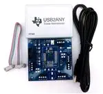
A computer with an available USB port is required to make use of the EVM software. The EVM software runs on
the computer and communicates with the EVM via the USB2ANY interface.
2.3 Power Supply
A DC power supply capable of delivering up to 5 V and 3 A, and a coin cell battery or separate 3-V power supply
for the backup supplies.
2
TPS65218EVM
SLVUAA6B – NOVEMBER 2014 – REVISED OCTOBER 2022
Submit Document Feedback
Copyright © 2022 Texas Instruments Incorporated
�www.ti.com
EVM Kit
3 EVM Kit
The EVM kit (Figure 3-1) contains the following items:
•
•
•
•
•
TPS65218 evaluation board
USB2ANY adapter
USB to USB micro cable
10-pin ribbon cable
30-pin ribbon cable
The 30-pin ribbon cable is not required for the TPS65218EVM.
Figure 3-1. TPS65218 EVM Kit
SLVUAA6B – NOVEMBER 2014 – REVISED OCTOBER 2022
Submit Document Feedback
Copyright © 2022 Texas Instruments Incorporated
TPS65218EVM
3
�Schematic
www.ti.com
4 Schematic
Figure 4-1 illustrates the schematic for this EVM.
JP3
VIO
VSYS
1
2
3
VSYS
VDCDC3
IN_LS1
R1
100k
IN_LS1_EXT 3
LS1
2
1
3
2
1
J1
GND
R6
100k
3
2
1
PWR_EN
JP1
S1
AC_DET
PB
1
4
2
3
JP5
GND
GND
GND
LS2
3
IN_LS2 2
C29
C30
DNP 68uF DNP 68uF
1
J2
GND
L5 0.11A
TP6
INT_LDO
C31
C32
DNP 68uF DNP 68uF
LS3
4
IN_LS3 3
LDO1 2
C9
0.1uF
GND
J3
VSYS
GND
VSYS
C27
DNP 470uF
4
3
2
1
GND
C17
10V
4.7uF
J4
VDCDC1
VDCDC2
VDCDC3
C11
10V
4.7uF
GND
4
3
2
1
C14
10V
4.7uF
GND
L3
0
R24
10
R22
IN_CC
R8 0
VSYS
C16
10uF
C5
10V
4.7uF
GND
2.8A
GND
GND
0
R5
VSYS
R11
L3
C18
10V
4.7uF
GND
VDCDC6
VDCDC5
VDCDC4
C4
16V
10uF
VDCDC3
4
3
2
1
GND
PFI
GND
L4
2.8A
C22
0.1uF
R12
100k
L4A
35
36
19
18
27
25
IN_LDO
LDO1
5
4
IN_LS1
LS1
31
30
IN_DC3 37
L3
38
VDCDC3 39
0
IN_DC4
L4A
L4B
VDCDC4
DC34_SEL
TP4
J6
GND
IN_BU
C8
10uF
GND
J5
VSYS
TP5
TP3
IN_nCC
VSYS
C19
10V
4.7uF
GND
IN_BIAS
PGOOD_BU
CC
GND
0
R23
C7
10V
4.7uF
CC
12
13
14
15
17
16
SCL
3
SDA
2
PWR_EN 46
AC_DET 9
PB
44
28
29
GND
C28
47uF
L6
INT_LDO
IN_BIAS
PGOOD_BU
L5
FB5
20
21 VDCDC5
L6
FB6
23
22 VDCDC6
IN_CC
IN_BU
24
IN_LS2
LS2
32
33
IN_LS2
LS2
IN_LS1
LS1
IN_LS3
LS3
6
7
IN_LS3
LS3
1
48
47
IN_DC1
L1
VDCDC1
IN_DCDC1
L1
FB1
IN_DCDC4
L4A
L4B
DCDC4
DC34_SEL
IN_DCDC2
L2
FB2
PFI
SCL
SDA
PWR_EN
AC_DET
PB
NC
NC
43
42
41
GPIO1
GPO2
GPIO3
POWER PAD
10
8
40
45
C26
10uF
GND
C10
10uF
R7
0
R3
0
IN_DC2
L2
VDCDC2
C13
25V
C15
10uF 4.7uF GND
C6
10V
GND
4.7uF GND
VSYS
VSYS
TP10
TP9
TP7
nPFO
R10
PGOOD
R9
nWAKEUP
R4
nINT
R2
11
34
26
GPIO1
49
GPO2
GPIO3
100k
100k
100k
100k
VIO
2
1
GND
L1
VIO
L2
GND
2.8A
GND
L2
VDCDC2
VIO
TP13
TP11
C1
16V
10uF
VDCDC1
VIO
TP12
2.8A
L1
C2
10V
4.7uF
R20 100k
R19 100k
R21 100k
GND
C20
10V
C12
1uF
10V
4.7uF GND
GND
TP8
PFO
PGOOD
WAKEUP
INT
C24
10uF
GND
C25
10uF
SYS_BU
IN_DCDC3
L3
FB3
0.11A
TP14
IN_LDO1
LDO1
CC
L4B
C21
0.1uF
C23
10uF
U1
TPS65218D0RSLR
1
VIO
C3
16V
10uF
GND
IN_LS1
VIO
GND
GND
JP2
VIO
J7
TP1
3
2
1
TP2
nWAKEUP
DNP
GPO2
R13 1.00k
DNP
R15 1.00k
AC_DET
DNP
R17 1.00k
GPIO7 1
GPIO5 3
V3p3 5
GPIO3 7
SCL 9
GND
GPIO6
GPIO4
GND
GPIO2
SDA
DNP
R14 1.00k
PWR_EN
DNP
R16 1.00k
DNP
R18 1.00k
GPIO3
GPIO1
N2510-6002-RB
JP4
GND
2
4
6
8
10
VDCDC4
VIO
GND
R25
4.75k
SCL
R26
4.75k
SDA
Figure 4-1. TPS65218 EVM Schematic
4
TPS65218EVM
SLVUAA6B – NOVEMBER 2014 – REVISED OCTOBER 2022
Submit Document Feedback
Copyright © 2022 Texas Instruments Incorporated
�www.ti.com
Terminal Block, Test Point, and Jumper Descriptions
5 Terminal Block, Test Point, and Jumper Descriptions
Table 5-1. Terminal Block Descriptions
Connector
J1
J2
J3
J4
J5
J6
J7
Pin
Description
Note
GND
Ground
—
LS1
LS1 Output
—
EXT
External supply to LS1
Power Input (1.2 V – 3.3 V)
GND
Ground
—
IN_LS2
LS2 Input
Power Input (3.0 V – 5.5 V)
LS2
LS2 Output
—
GND
Ground
—
LDO1
LDO1 Output
Default 1.8 V
IN_LS3
LS3 Input
Power Input (1.8 V – 9.9 V)
LS3
LS3 Output
—
GND
Ground
—
GND
Ground
—
VSYS
DC Input
Power Input (2.7 V – 5.5 V)
CC
Coin Cell Battery Input
Power Input (2.2 V – 3.3 V)
GND
Ground
—
DC3
Buck 3 Output (DCDC3)
Default 1.2 V Output
DC2
Buck 2 Output (DCDC2)
Default 1.1 V Output
DC1
Buck 1 Output (DCDC1)
Default 1.1 V Output
GND
Ground
—
DC4
Buck-Boost Output (DCDC4)
Default 3.3 V Output
DC5
Battery Backup Supply Output (DCDC5)
1.0 V Output
DC6
Battery Backup Supply Output (DCDC6)
1.8 V Output
10-pin EVM connector for USB2ANY cable (I2C communication)
Table 5-2. Test Point Descriptions(1)
Test Point
GND
INT_LDO
nWAKEUP
Ground
Internal bias voltage
Wakeup output signal
nINT
Interrupt output
nPFO
Power-fail comparator output
GPO2
General purpose output 2 or DDR reset output
GPIO3
General purpose output 3 or warm reset input
PGOOD
GPIO1
SYS_BU
PFI
IN_nCC
PGOOD_BU
(1)
Description
Power good
General purpose output 1
Battery back-up power path output
Power-fail comparator input
Output indicating power source for battery backup supplies
Power good for backup supplies
Test points are not designed to carry current, they are intended for measuring voltage.
Table 5-3. Jumper Descriptions
Jumper
Description
Default Position
JP1
Ties PWR_EN to VIO or GND
PWR_EN tied to VIO
JP2
Ties DC34_SEL pin to ground. Remove and jump with resistor for alternate voltage
selections.
DC34_SEL tied to GND
SLVUAA6B – NOVEMBER 2014 – REVISED OCTOBER 2022
Submit Document Feedback
Copyright © 2022 Texas Instruments Incorporated
TPS65218EVM
5
�Terminal Block, Test Point, and Jumper Descriptions
www.ti.com
Table 5-3. Jumper Descriptions (continued)
Jumper
6
Description
Default Position
JP3
Selects LS1 input between DCDC3 output and external supply from J1
IN_LS1 tied to DC3
JP4
Ties VIO to either DCDC4 output or 3.3-V supply from USB2ANY adaptor (J9). VIO
supplies the pull-up voltage for the device I/Os.
VIO tied to V3p3
JP5
Ties AC_DET pin to either VSYS or GND. Tying to GND causes the device to start upon
VSYS application.
AC_DET tied to VSYS
TPS65218EVM
SLVUAA6B – NOVEMBER 2014 – REVISED OCTOBER 2022
Submit Document Feedback
Copyright © 2022 Texas Instruments Incorporated
�www.ti.com
Setup
6 Setup
Figure 6-1 displays an example setup for using the TPS65218 EVM.
+
DCDC1 Load
-
5V Supply
+
-
3V Supply
+
-
USB2ANY
Figure 6-1. TPS65218 EVM Setup
SLVUAA6B – NOVEMBER 2014 – REVISED OCTOBER 2022
Submit Document Feedback
Copyright © 2022 Texas Instruments Incorporated
TPS65218EVM
7
�Software
www.ti.com
7 Software
7.1 Software Installation Instruction
A GUI is supplied to provide a simple way to communicate to the device via I2C. The GUI can be downloaded
from: IPG-UI EVM GUI
Information on the installation of the IPG-UI can be found in the IPG-UI User's Guide.
You will also need to download the BOOSTXL-TPS65218 IPG-UI Device Support File. After you finish setting up
the IPG-UI software, run the installer associated with your operating system to add the TPS65218 device file to
your IPG-UI device library.
7.2 Using the TPS65218 GUI
Detailed information regarding the usage of the IPG-UI can also be found in the IPG-UI User's Guide. A brief
overview is provided here for reference.
The proper device must first be selected from the "Select Devices" drop-down menu.
Figure 7-1. GUI front Page
8
TPS65218EVM
SLVUAA6B – NOVEMBER 2014 – REVISED OCTOBER 2022
Submit Document Feedback
Copyright © 2022 Texas Instruments Incorporated
�www.ti.com
Software
From there, the next screen is the device introduction page, which includes a brief overview as well as the
functional block diagram for the device.
Figure 7-2. GUI Device Introduction
Finally, clicking on "Get Started" or on "Register Map" takes you to the I2C controls for the device sorted by
register address.
Figure 7-3. GUI Register Map
SLVUAA6B – NOVEMBER 2014 – REVISED OCTOBER 2022
Submit Document Feedback
Copyright © 2022 Texas Instruments Incorporated
TPS65218EVM
9
�Software
www.ti.com
Alternatively, the part can be controlled using the "Register Controls" tab to sort by functionality rather than by
I2C address location.
Figure 7-4. GUI Register Controls
With this information, it is possible to begin evaluating the TPS65218 device.
10
TPS65218EVM
SLVUAA6B – NOVEMBER 2014 – REVISED OCTOBER 2022
Submit Document Feedback
Copyright © 2022 Texas Instruments Incorporated
�www.ti.com
Bill of Materials
8 Bill of Materials
Table 8-1 lists the BOM for this EVM.
Table 8-1. Bill of Materials
Designator
Description
Value
Voltage
Rating
Dielectric Footprint
Qty.
Manufacturer
Manufacturer PN
C1, C3, C4
Capacitor
10µ
16V
X5R
805
3
MuRata
GRM21BR61C106KE15L
C8
Capacitor
10µ
6.3 V
X7R
805
1
TDK
C2012X7R0J106K125AB
C2, C5–C7, C11,
C12, C14, C17–
C19
Capacitor
4.7µ
10V
X7R
805
10
TDK
C2012X7R1A475K125AC
C10, C16, C23–
C26
Capacitor
10µ
10V
X7R
805
6
TDK
C2012X7R1A106K125AC
C9, C21, C22
Capacitor
100n
100V
X5R
805
3
TDK
C2012X5R2A104K125AA
C13
Capacitor
4.7µ
25V
X5R
805
1
TDK
C2012X5R1E475K125AB
C15
Capacitor
10µ
16V
X7R
805
1
Samsung
CL21B106KOQNNNE
C28
Capacitor
47µ
10V
X5R
805
1
TDK
C2012X5R1A476M125AC
C20
Capacitor
1µ
10V
X7R
805
1
TDK
C2012X7R1A105K
C27
Capacitor
470µ
25V
CAP_EEE Size G
0
Panasonic
EEE1EA471UAP
C29, C30, C31,
C32
Capacitor
68µ
16V
6032
0
Kemet
B45197A3686+30
L1, L2, L3, L4
Inductor
1.5µ
IND_SPM3012
4
TDK
SPM3012T-1R5M
L5, L6
Inductor
10µ
805
2
TDK
MLZ2012N100LT
R1, R2, R4, R6,
R9, R10, R12,
R19, R20, R21
Resistor
100K
603
10
Vishay-Dale
CRCW0603100KFKEA
R3, R5, R7, R8,
R11, R23, R24
Resistor
0
805
7
Vishay-Dale
CRCW08050000Z0EAHP
R13–R18
Resistor
1K
603
0
Vishay-Dale
CRCW06031K00FKEA
R22
Resistor
10
603
1
Vishay-Dale
CRCW060310R0JNEAHP
R25, R26
Resistor
4.75K
603
2
Vishay-Dale
CRCW06034K75FKEA
S1
Switch
6.3x5.36x6.6 mm
1
C&K Components
KT11P2JM34LFS
U1
PMIC
RSL (S-PQFP-N48) 0.4
pitch
1
Texas Instruments
TPS65218D0
32V
SLVUAA6B – NOVEMBER 2014 – REVISED OCTOBER 2022
Submit Document Feedback
Copyright © 2022 Texas Instruments Incorporated
TPS65218EVM
11
�Layout
www.ti.com
9 Layout
Figure 9-1 through Figure 9-6 illustrate the PCB layouts for the evaluation module.
Figure 9-1. Top Layer Silkscreen
Figure 9-2. Top Layer
12
TPS65218EVM
SLVUAA6B – NOVEMBER 2014 – REVISED OCTOBER 2022
Submit Document Feedback
Copyright © 2022 Texas Instruments Incorporated
�www.ti.com
Layout
Figure 9-3. Ground Plane
Figure 9-4. Mid Layer
SLVUAA6B – NOVEMBER 2014 – REVISED OCTOBER 2022
Submit Document Feedback
Copyright © 2022 Texas Instruments Incorporated
TPS65218EVM
13
�Layout
www.ti.com
Figure 9-5. Bottom Layer
Figure 9-6. Bottom Layer Silkscreen
14
TPS65218EVM
SLVUAA6B – NOVEMBER 2014 – REVISED OCTOBER 2022
Submit Document Feedback
Copyright © 2022 Texas Instruments Incorporated
�www.ti.com
Revision History
10 Revision History
NOTE: Page numbers for previous revisions may differ from page numbers in the current version.
Changes from Revision A (August 2022) to Revision B (October 2022)
Page
• Updated EVM Schematic....................................................................................................................................4
• Updated Bill of Materials................................................................................................................................... 11
Changes from Revision * (November 2014) to Revision A (August 2022)
Page
• Updated the numbering format for tables, figures, and cross-references throughout the document..................1
• Changed GUI description................................................................................................................................... 2
• Updated link to software..................................................................................................................................... 2
• Changed links to GUI and supporting hardware.................................................................................................8
• Updated descriptions.......................................................................................................................................... 8
• Changed topic title.............................................................................................................................................. 8
• Changed steps to use GUI................................................................................................................................. 8
• Added new images............................................................................................................................................. 8
• Updated software links....................................................................................................................................... 8
SLVUAA6B – NOVEMBER 2014 – REVISED OCTOBER 2022
Submit Document Feedback
Copyright © 2022 Texas Instruments Incorporated
TPS65218EVM
15
�IMPORTANT NOTICE AND DISCLAIMER
TI PROVIDES TECHNICAL AND RELIABILITY DATA (INCLUDING DATA SHEETS), DESIGN RESOURCES (INCLUDING REFERENCE
DESIGNS), APPLICATION OR OTHER DESIGN ADVICE, WEB TOOLS, SAFETY INFORMATION, AND OTHER RESOURCES “AS IS”
AND WITH ALL FAULTS, AND DISCLAIMS ALL WARRANTIES, EXPRESS AND IMPLIED, INCLUDING WITHOUT LIMITATION ANY
IMPLIED WARRANTIES OF MERCHANTABILITY, FITNESS FOR A PARTICULAR PURPOSE OR NON-INFRINGEMENT OF THIRD
PARTY INTELLECTUAL PROPERTY RIGHTS.
These resources are intended for skilled developers designing with TI products. You are solely responsible for (1) selecting the appropriate
TI products for your application, (2) designing, validating and testing your application, and (3) ensuring your application meets applicable
standards, and any other safety, security, regulatory or other requirements.
These resources are subject to change without notice. TI grants you permission to use these resources only for development of an
application that uses the TI products described in the resource. Other reproduction and display of these resources is prohibited. No license
is granted to any other TI intellectual property right or to any third party intellectual property right. TI disclaims responsibility for, and you
will fully indemnify TI and its representatives against, any claims, damages, costs, losses, and liabilities arising out of your use of these
resources.
TI’s products are provided subject to TI’s Terms of Sale or other applicable terms available either on ti.com or provided in conjunction with
such TI products. TI’s provision of these resources does not expand or otherwise alter TI’s applicable warranties or warranty disclaimers for
TI products.
TI objects to and rejects any additional or different terms you may have proposed. IMPORTANT NOTICE
Mailing Address: Texas Instruments, Post Office Box 655303, Dallas, Texas 75265
Copyright © 2022, Texas Instruments Incorporated
�