www.ti.com
Table of Contents
User’s Guide
TPS65251 Buck Converter Evaluation Module User's
Guide
Table of Contents
1 Introduction.............................................................................................................................................................................2
2 Background.............................................................................................................................................................................3
3 Schematic................................................................................................................................................................................4
4 Placement (Top Layer)............................................................................................................................................................6
5 Bench Test Setup Conditions................................................................................................................................................ 7
5.1 Headers Description and Jumper Placement.....................................................................................................................7
5.2 Jumpers..............................................................................................................................................................................8
5.3 Test Points and Placement.................................................................................................................................................8
6 Power-Up Procedure.............................................................................................................................................................. 9
7 Bill of Materials..................................................................................................................................................................... 10
8 Revision History....................................................................................................................................................................11
Trademarks
All trademarks are the property of their respective owners.
SLVU399B – AUGUST 2010 – REVISED MAY 2021
Submit Document Feedback
TPS65251 Buck Converter Evaluation Module User's Guide
Copyright © 2021 Texas Instruments Incorporated
1
�Introduction
www.ti.com
1 Introduction
This document presents the information required to power the TPS65251 PMIC as well as the support
documentation including schematic and bill of materials.
2
TPS65251 Buck Converter Evaluation Module User's Guide
Copyright © 2021 Texas Instruments Incorporated
SLVU399B – AUGUST 2010 – REVISED MAY 2021
Submit Document Feedback
�www.ti.com
Background
2 Background
The TPS65251 PMIC is designed to provide 3-A and 2-A continuous outputs with an operational range of 4.5 V
to 18 V and an externally set switching frequency ranging from 300 kHz to 2.2 MHz. When the PMIC is not fully
loaded, Buck1 can be loaded to 3.5 A and Buck2 and Buck3 to 2.5 A.
As there are many possible options to set the converters, Table 2-1 presents the performance specification
summary for the EVM.
Table 2-1. Input Voltage and Output Current Summary
EVM
TEST CONDITIONS
OUTPUT CURRENT RANGE
Buck1, 1.2 V, 3 A
TPS65251EVM
Buck2, 1.8 V, 2 A
VIN = 4.5 V to 13 V
fsw = 500 kHz
Buck3, 3.3 V, 2 A
(25°C ambient)
This evaluation module is designed to provide access to the features of the TPS65251. Some modifications
can be made to this module to test performance at different input and output voltages, current and frequency
operation. Please contact TI Field Applications Group for advice on these matters.
SLVU399B – AUGUST 2010 – REVISED MAY 2021
Submit Document Feedback
TPS65251 Buck Converter Evaluation Module User's Guide
Copyright © 2021 Texas Instruments Incorporated
3
�Schematic
www.ti.com
3 Schematic
See next page.
The resistor and capacitor values have been chosen according to the guidelines presented on the TPS65251
spec available at http://focus.ti.com/docs/prod/folders/print/tps65251.html.
Note that for the purpose of gains-phase measurements R10, R19 and R21 (0 Ω on the EVM) need to be
replaced by suitable low value resistors as per the network analyzer setup required. Test points are provided on
either end of the resistors to allow for easy measurement.
4
TPS65251 Buck Converter Evaluation Module User's Guide
Copyright © 2021 Texas Instruments Incorporated
SLVU399B – AUGUST 2010 – REVISED MAY 2021
Submit Document Feedback
�J1
3
2
1
R12
80.6K
R9
40.2K
TP10
FB1A
R19
0
VOUT1
GND
4.7nF
C13
TP5
1.2V@3A
FB1
GND
GND
VOUT1
J3
2
FB2
GND
V3V
R15
32.4K
40.2K
R11
TP16
FB2A
R21
0
VOUT2
TP12
VOUT2
GND
4.7nF
C18
1.8V@2A
1
GND
VOUT2
J2
VOUT1
GND
C16
22uF
4.7uH
L2
TDK-SLF7055
4.7uH
L1
TDK-SLF7055
C12
22uF
GND
C5
4.7nF
GND
JP2
GND
VIN
C7
VIN
C10 10uF
47nF
47nF
41
20
19
18
17
16
15
14
13
12
11
Pin 25 SDA
and Pin 26
SCLK access
GND
C24
C17 10uF
C29
4.7nF
GND
GND
JP4
GND
ENB1
PwrPad
EN2
BST2
VIN2
LX2
LX2
LX1
LX1
VIN1
BST1
EN1
C4
R16
120K
GND
4.7nF
C25
R7
383K
R17
20K
4.7nF
R3
20K
1.2V@3A
GND GND
GND
C26
C27
3.3uF
TP28 GND
V3V
U1
GND
VIN
VIN
VIN
GND
LX3
LX3
VIN3
BST3
EN3
4.7nF R4
120K
TP27V7V TP29
10uF
JP6
GND
4.7nF C3
R18
PGOOD
C20
JP5
GND
C14 C1
JP1
FB3
GND
TPS65251
FB2
C28
GND
C19
FB1
4.7nF
C2
GND
100K 4.7nF R5
20K
R1
GND
9
1
V3V
10
RLIM1
RLIM2
21
SS1
SS2
22
8
23
2
LOW_P (SDA)
25
CMP1
COMP2
6
DNI
GND
26
1
DNI
DNI
GND (SCLK)
7
FB1
FB2
24
ROSC
5
SYNC
4
FB3
PGOOD
27
2
100K
Copyright © 2021 Texas Instruments Incorporated
PGOOD
3
COMP3
V7V
28
SS3
V3V
29
RLIM3
AGND
30
SLVU399B – AUGUST 2010 – REVISED MAY 2021
Submit Document Feedback
AGND
VIN
31
32
33
34
35
36
37
38
39
40
C8
GND
C9
VIN
4.7uH
L3
TDK-SLF7055
GND
10uF
C30
GND
TP33 VIN
GND
10uF
47nF
ENB3
V3V
GND
22uF
C11
3.31V@2A
GND GND
C6
4.7nF
JP3
TP8
FB3A
TP4
VOUT3
R13
12.7K
FB3
R20
40.2K
R10
0
GND
4.7nF
C15
VOUT3
VOUT3
J6
GND
GND
GND
GND
GND
2
1
TP15
TP14
TP2
TP1
GND
www.ti.com
Schematic
Figure 3-1. TPS65251 Schematic
TPS65251 Buck Converter Evaluation Module User's Guide
5
�Placement (Top Layer)
www.ti.com
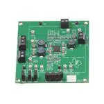
4 Placement (Top Layer)
Figure 4-1. Placement (Top Layer)
6
TPS65251 Buck Converter Evaluation Module User's Guide
Copyright © 2021 Texas Instruments Incorporated
SLVU399B – AUGUST 2010 – REVISED MAY 2021
Submit Document Feedback
�Bench Test Setup Conditions
www.ti.com
5 Bench Test Setup Conditions
5.1 Headers Description and Jumper Placement
Vin
4.5V – 18V
Vout 3
Vout_1
+
+
Vout 2
+
SYNC
LOW P
SCLK
EN 1
Vout 1
EN 2
Vout 2
EN 3
Vout 3
Figure 5-1. Headers Description and Jumper Placement
Test points:
Black – GND
White – Each output, feed-back, power good and VIN. All marking on PCB.
SLVU399B – AUGUST 2010 – REVISED MAY 2021
Submit Document Feedback
TPS65251 Buck Converter Evaluation Module User's Guide
Copyright © 2021 Texas Instruments Incorporated
7
�Bench Test Setup Conditions
www.ti.com
5.2 Jumpers
Table 5-1. Jumpers
JUMPER
NO.
FUNCTION
PLACEMENT
COMMENT
JP1
SYNC input
For buck internal clock fit jumper.
For external SYNC connect as per drawing.
Jumper must be fitted if no external SYNC
is used
JP2
Buck1 enable (EN1)
For automatic start-up fit jumper to V3V.
For sequencing do not fit jumper.
To disable converter fit jumper to GND.
Fit according to test requirement
JP3
Buck3 enable (EN3)
For automatic start-up fit jumper to V3V.
For sequencing do not fit jumper.
To disable converter fit jumper to GND.
Fit according to test requirement
JP4
Buck2 enable (EN2)
For automatic start-up fit jumper to V3V.
For sequencing do not fit jumper.
To disable converter fit jumper to GND.
Fit according to test requirement
JP5
LOW_P
Low power: Power save mode ON/OFF. If need
low power mode test, should connect V3V internal
regulator test point (TP29).
Fit according to test requirement. During
normal operation jumper must be fitted.
JP6
GND
For normal operation fit jumper (GND)
Fit according to test requirement. During
normal operation jumper must be fitted.
5.3 Test Points and Placement
Buck converter outputs are red and have a label for easy location. Close to any of these test points there are
black ground test points to allow for DVM measurement or to use a metal exposed scope probe to reduce
common mode noise measurements. All test points are described in Table 5-2.
Table 5-2. Test Points and Placement
TEST
POINT
8
NAME
SIGNAL
COLOR
TP1
GND
Ground
Black
TP2
GND
Ground
Black
COMMENT
TP3
AGND
Ground
TP4
VOUT3
Buck3 output
White
Not fitted. Only Via.
TP5
VOUT1
Buck1 output
White
TP8
FB3A
Input for gain-phase measurement Buck3
White
Normally not used
TP10
FB1A
Input for gain-phase measurement Buck1
White
Normally not used
TP12
VOUT2
Buck2 output
White
Normally not used
TP14
GND
Ground
Black
TP15
GND
Ground
Black
TP16
FB2A
Input for gain-phase measurement Buck2
White
TP27
PGOOD
Power Good (open drain connected to Buck1 output)
White
TP28
V7V
V7V pin (internal rail)
White
TP29
V3V
V3V pin (internal rail)
White
TP33
VIN
Input supply
White
TPS65251 Buck Converter Evaluation Module User's Guide
Copyright © 2021 Texas Instruments Incorporated
Normally not used
SLVU399B – AUGUST 2010 – REVISED MAY 2021
Submit Document Feedback
�www.ti.com
Power-Up Procedure
6 Power-Up Procedure
1. Define which converters are to be enabled or disabled by connecting the correct jumpers accordingly
(enable to V3V, disable to GND for all cases).
2. Apply a DC voltage to jumper J3. Polarity is clearly marked on the silk-screen.
3. Verify that the relevant converters are powered up by the output voltages. The whole start-up process will
take around 100 ms. PGOOD will be asserted after 1 s.
4. Apply loads to the output connectors.
5. For low power and SYNC operation remove the jumpers and connect control supplies as indicated in the
bench test setup section.
SLVU399B – AUGUST 2010 – REVISED MAY 2021
Submit Document Feedback
TPS65251 Buck Converter Evaluation Module User's Guide
Copyright © 2021 Texas Instruments Incorporated
9
�Bill of Materials
www.ti.com
7 Bill of Materials
Table 7-1. Bill of Materials
10
ITEM
QUANTITY
DESIGNATOR
VALUE
FOOTPRINT
MANUFACTURER
MANUFACTURER
PART NO.
DESCRIPTION
COMMENT
1
9
C1, C2, C3,
C4, C5, C6,
C25, C28, C29
4.7 nF
603
Panasonic -ECG
ECJ-1VB1H472K
4700PF 50V
X7R 0603
Ceramic capacitor
2
3
C7, C8, C24
47 nF
603
Panasonic -ECG
ECJ-1VF1H473Z
47000PF 50V
Y5V 0603
Ceramic capacitor
3
3
C9, C10, C17
10 µF
1206
Panasonic -ECG
ECJ-3YB1E106M
10UF 25V X5R
1206
Ceramic capacitor
4
3
C11, C12, C16
22 µF
1210
Panasonic -ECG
ECJ-4YB1E226M
22UF 25V X5R
1210
Ceramic capacitor
5
3
C13, C15, C18
470 pF
603
Panasonic -ECG
ECJ-1VB2A471K
470PF 100V
X7R 0603
Ceramic capacitor
6
3
C14, C19, C20
DNI
603
Ceramic capacitor
Capacitor
7
1
C26
10 µF
805
Panasonic -ECG
ECJ-2FB1A106K
10UF 10V X5R
0805
8
1
C27
3.3 µF
603
TDK
C1608X5R1A335K
3.3UF 10V X5R
0603
Ceramic capacitor
9
1
C30
10 µF
1206
Panasonic -ECG
ECJ-3YB1E106M
10UF 25V, X5R
1206
Ceramic capacitor
10
1
J1
TB_3X3.5MM
OnShoreTechnology Inc
ED555/3DS
Terminal,
3 pin, 6 A,
3.5 mm
VOUT1
11
1
J2, J3, J6
TB_2X3.5MM
OnShoreTechnology Inc
ED555/2DS
Terminal,
2 pin, 6 A,
3.5 mm
TBLK_6A_2X3.5MM
12
3
JP1, JP5, JP6
JMP0.2
Mil-Max
800-10-064-10-0010
00
SIP HEADER
STRAIGHT
PCB
JUMPER 2 PIN
13
3
JP2, JP3, JP4
JMP0.3
Mil-Max
800-10-064-10-0010
00
SIP HEADER
STRAIGHT
PCB
JUMPER 2 PIN
14
3
L1, L2, L3
4.7 µH
IND_SLF7055
TDK Corporation
SLF7055T-4R7N3R
1-3PF
Magnetic-Core
Inductor
TDK-SLF7055
15
2
R1, R18
100 kΩ
603
Panasonic -ECG
ERA-3AEB104V
RES 100 kΩ
1/10 W .1%
0603 SMD
Resistor
16
3
R3, R5, R17
20 kΩ
603
Panasonic -ECG
ERA-3YEB203V
RES 20 kΩ
1/10 W .1%
0603 SMD
Resistor
17
2
R4, R16
150 kΩ
603
Panasonic -ECG
ERJ-3EKF1503V
RES 150 kΩ
1/10 W 1%
0603 SMD
Resistor
18
1
R7
383 kΩ
603
Panasonic -ECG
ERJ-3EKF3833V
RES 383 kΩ
1/10 W 1%
0603 SMD
Resistor
19
1
R8
DNI
603
Panasonic -ECG
ERJ-3GEY0R00V
RES ZERO Ω
1/10 W 5%
0603 SMD
Resistor
20
3
R9, R11, R20
360 kΩ
603
Panasonic -ECG
ERJ-3EKF3603V
RES 360 kΩ
1/10 W 1%
0603 SMD
Res1
21
3
R10, R19, R21
49.9 Ω
603
Susumu Co Ltd
RR0816Q-49R9D-68R
RES 49.9 Ω
1/16 W .5%
0603 SMD
Res1
22
1
R12
715 kΩ
603
Panasonic -ECG
ERJ-3EKF7153V
RES 715 kΩ
1/10 W 1%
0603 SMD
Resistor
23
1
R13
115 kΩ
603
Panasonic -ECG
ERJ-3EKF1153V
RES 115 kΩ
1/10 W 1%
0603 SMD
Resistor
24
1
R15
287 kΩ
603
Panasonic -ECG
ERJ-3EKF2873V
RES 287 kΩ
1/10 W 1%
0603 SMD
Resistor
TPS65251 Buck Converter Evaluation Module User's Guide
Copyright © 2021 Texas Instruments Incorporated
SLVU399B – AUGUST 2010 – REVISED MAY 2021
Submit Document Feedback
�www.ti.com
Revision History
Table 7-1. Bill of Materials (continued)
ITEM
QUANTITY
DESIGNATOR
VALUE
FOOTPRINT
MANUFACTURER
MANUFACTURER
PART NO.
DESCRIPTION
COMMENT
25
4
TP1, TP2,
TP14, TP15,
Black
TEST POINT
0.052
Keystone
5001
TEST POINT
MINI .040"D
BLACK
GND
26
1
TP3
STD
TP-SMALL
27
1
TP4, TP5, TP8,
TP10, TP12,
TP16, TP27,
TP28, TP29,
TP33
TEST POINT
0.052
Keystone
28
1
U1
QFN-40
TI
Test Point, 0.020 Hole
5002
TEST POINT
MINI .040"D
WHITE
Glass Beaded Test
Point
TPS65251
8 Revision History
NOTE: Page numbers for previous revisions may differ from page numbers in the current version.
Changes from Revision A (August 2010) to Revision B (May 2021)
Page
• Updated user's guide title................................................................................................................................... 2
• Updated the numbering format for tables, figures, and cross-references throughout the document. ................2
SLVU399B – AUGUST 2010 – REVISED MAY 2021
Submit Document Feedback
TPS65251 Buck Converter Evaluation Module User's Guide
Copyright © 2021 Texas Instruments Incorporated
11
�IMPORTANT NOTICE AND DISCLAIMER
TI PROVIDES TECHNICAL AND RELIABILITY DATA (INCLUDING DATA SHEETS), DESIGN RESOURCES (INCLUDING REFERENCE
DESIGNS), APPLICATION OR OTHER DESIGN ADVICE, WEB TOOLS, SAFETY INFORMATION, AND OTHER RESOURCES “AS IS”
AND WITH ALL FAULTS, AND DISCLAIMS ALL WARRANTIES, EXPRESS AND IMPLIED, INCLUDING WITHOUT LIMITATION ANY
IMPLIED WARRANTIES OF MERCHANTABILITY, FITNESS FOR A PARTICULAR PURPOSE OR NON-INFRINGEMENT OF THIRD
PARTY INTELLECTUAL PROPERTY RIGHTS.
These resources are intended for skilled developers designing with TI products. You are solely responsible for (1) selecting the appropriate
TI products for your application, (2) designing, validating and testing your application, and (3) ensuring your application meets applicable
standards, and any other safety, security, regulatory or other requirements.
These resources are subject to change without notice. TI grants you permission to use these resources only for development of an
application that uses the TI products described in the resource. Other reproduction and display of these resources is prohibited. No license
is granted to any other TI intellectual property right or to any third party intellectual property right. TI disclaims responsibility for, and you
will fully indemnify TI and its representatives against, any claims, damages, costs, losses, and liabilities arising out of your use of these
resources.
TI’s products are provided subject to TI’s Terms of Sale or other applicable terms available either on ti.com or provided in conjunction with
such TI products. TI’s provision of these resources does not expand or otherwise alter TI’s applicable warranties or warranty disclaimers for
TI products.
TI objects to and rejects any additional or different terms you may have proposed. IMPORTANT NOTICE
Mailing Address: Texas Instruments, Post Office Box 655303, Dallas, Texas 75265
Copyright © 2022, Texas Instruments Incorporated
�