TPS65281, TPS65281-1
www.ti.com
SLVSBH7B – JULY 2012 – REVISED DECEMBER 2012
PRECISION ADJUSTABLE CURRENT LIMITED POWER DISTRIBUTION SWITCH WITH 4.5V
TO 18V INPUT VOLTAGE, 3A OUTPUT CURRENT SYNCHRONOUS BUCK REGULATOR
Check for Samples: TPS65281, TPS65281-1
FEATURES
1
INTEGRATED POWER DISTRIBUTION SWITCH
•
•
•
•
•
•
•
•
Operating Input Voltage Range: 2.5 V to 6.5 V
Adjustable Current Limit:
75 mA - 2.7 A (typical)
±6% Current-Limit Accuracy at 1.7 A (typical)
Over Current Latch-Off Protection (TPS65281)
and Over Current Auto-Recovery (TPS65281-1)
Reverse Input-Output Voltage Protection
Built-In Soft-Start
Integrated Back-to-Back Power MOSFETs With
100-mΩ On-Resistance
Over Temperature Protection
xxx
xxx
xxx
xxx
xxx
xxx
xxx
xxx
xxx
•
•
•
•
•
•
•
•
INTEGRATED BUCK CONVERTER
Wide Input Voltage Range: 4.5 V to 18 V
Maximum Continuous 3-A Output Current
Feedback Reference Voltage: 0.8 V ±1 %
Adjustable 300-kHz to 1.4-MHz Switching
Frequency
Adjustable Soft Start and Tracking With
Built-In 1-ms Internal Soft-Start Time
Cycle-by-Cycle Current Limit
Output Over-voltage Protection
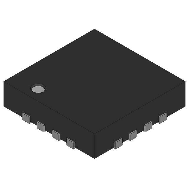
16-Lead QFN (RGV) 4-mm x 4-mm Package
APPLICATIONS
•
•
•
•
•
USB Ports and Hubs
Digital TV
Set-Top Boxes
VOIP Phones
Tablet PC
DESCRIPTION/ORDERING INFORMATION
The TPS65281/TPS65281-1 incorporates an N-channel back-to-back power MOSFET switch and a monolithic
buck converter. The device is intended to provide a total power distribution solution for digital TV, set-top boxes,
tablet PC and VOIP phones etc applications, where precision current limiting is required or heavy capacitive load
or short circuit are encountered.
A 100-mΩ independent power distribution switch limits the output current to a programmable current limit
threshold between typical 75 mA and 2.7 A by using an external resistor. The current limit accauracy as tight as
±6% can be achieved at higher current limit setting. TPS65281 provides circuit breaker functionality by latching
off the power switch during over-current or reverse-voltage situations. TPS65281-1 limits output current to a safe
level by using a constant current mode when the output load exceeds the current limit threshold. An internal
reverse-voltage comparator disables the power switch when the output voltage is driven higher than the input to
protect the device on the input side of the switch in normal operation. The nFAULT output asserts low under
over-current and reverse-voltage conditions. Back-to-back power MOSFETs structure prevents the reverse
current injection from an active load at output port during shutdown of power switch.
1
Please be aware that an important notice concerning availability, standard warranty, and use in critical applications of
Texas Instruments semiconductor products and disclaimers thereto appears at the end of this data sheet.
PRODUCTION DATA information is current as of publication date.
Products conform to specifications per the terms of the Texas
Instruments standard warranty. Production processing does not
necessarily include testing of all parameters.
Copyright © 2012, Texas Instruments Incorporated
�TPS65281, TPS65281-1
SLVSBH7B – JULY 2012 – REVISED DECEMBER 2012
www.ti.com
The buck DC/DC converter integrates power MOSFETs for optimized power efficiency and reduced external
component count. A wide 4.5-V to 18-V input supply range to buck encompasses most intermediate bus voltages
operating off 5-V, 9-V, 12-V or 15-V power bus. Constant frequency peak current mode control simplifies the
compensation and provides fast transient response. The buck can be precisely sequenced and ramp up in order
to align with other rails in the system with the soft-start pin. With SS pin floating, the built-in 1ms soft-start time
prevents in-rush current. Cycle-by-cycle over current protection and hiccup operation limit MOSFET power
dissipation in short circuit or over loading fault conditions. The switching frequency of the converter can be
programmed from 300 kHz to 1.4 MHz with an external resistor at ROSC pin. With ROSC pin connecting to V7V
pin, floating, or grounding, a default fixed switching frequency can be selected to reduce an external resistor.
The TPS65281/TPS65281-1 is available in a 16-lead thermally enhanced QFN (RGV) 4-mm x 4-mm thin
package.
ORDERING INFORMATION (1)
TA
PACKAGE
(2)
ORDERABLE PART NUMBER
TPS65281RGVR
–40°C to 85°C
16-Pin QFN (RGV)
TPS65281RGVT
TPS65281-1RGVR
TPS65281-1RGVT
(1)
(2)
2
TOP-SIDE MARKING
TPS65281
TPS65281-1
For the most current package and ordering information, see the Package Option Addendum at the end of this document, or see the TI
web site at www.ti.com.
Package drawings, thermal data, and symbolization are available at www.ti.com/packaging.
Submit Documentation Feedback
Copyright © 2012, Texas Instruments Incorporated
Product Folder Links: TPS65281 TPS65281-1
�TPS65281, TPS65281-1
www.ti.com
SLVSBH7B – JULY 2012 – REVISED DECEMBER 2012
This integrated circuit can be damaged by ESD. Texas Instruments recommends that all integrated circuits be handled with
appropriate precautions. Failure to observe proper handling and installation procedures can cause damage.
ESD damage can range from subtle performance degradation to complete device failure. Precision integrated circuits may be more
susceptible to damage because very small parametric changes could cause the device not to meet its published specifications.
TYPICAL APPLICATION
C7
47nF
L1
4.7uH
+5V
C6
4.7nF
R3
40.2kΩ
C5
22uF
13
14
9
10
SW_IN
C4
10uF
7
AGND
VIN
USB Data
8
USB
Port
TPS65281
EN
EN_SW
6
USB fault signal
5
RLIM
USB control signal
4
1
2
SS
16
nFAULT
ROSC
C2
1uF
V7V
3
15
Enable
R5
100kΩ
SW_OUT
PGND
COMP
VIN
6V~18V
C1
10uF
FB
BST
LX
11
12
R4
7.68kΩ
C3
4.7nF
R2
20kΩ
R1
10kΩ
Figure 1. 12-V Power Bus
L1
4.7uH
C7
47nF
+3.3V
C6
4.7nF
R3
40.2kΩ
C5
22uF
13
9
SW_IN
11
10
FB
R5
100kΩ
SW_OUT
8
AGND
7
C1
10uF
14
VIN
USB Data
C4
10uF
USB
Port
TPS65281
EN_SW
5
USB fault signal
USB control signal
4
1
C3
4.7nF
6
RLIM
EN
ROSC
nFAULT
3
16
V7V
SS
C2
1uF
COMP
15
Enable
PGND
2
VIN
5V
LX
BST
12
R4
12.7kΩ
R2
20kΩ
R1
10kΩ
Figure 2. 5-V Power Bus
Submit Documentation Feedback
Copyright © 2012, Texas Instruments Incorporated
Product Folder Links: TPS65281 TPS65281-1
3
�TPS65281, TPS65281-1
SLVSBH7B – JULY 2012 – REVISED DECEMBER 2012
www.ti.com
FUNCTION BLOCK DIAGRAM
V7V
15
14
LDO
5V
VIN
Voltage Reference
Current Bias
Preregulator
HS current sensing
1 .25 M
CS
12
1 .25 M
EN
BST
16
enable buffer
HS driver
Current Sensing
(0 .1 V/A)
COMP
FB
11
Buck
Controller
2
PWM comparator
LX
V7V
slope
comp
10
LS driver
0 .8 V
SS
1
error amplifer
CS
LS current sensing
V7 V
10 uA
ROSC
SW_IN
3
1 ms
Internal
Soft Start
13
Oscillotor
BUCK
POWER SWITCH
9
PGND
7
AGND
UVLO
POR
reverse voltage
comparator
8
CS
SW_OUT
current sensing
Charge
Pump
1. 25M
4 ms Degl .
Time
Driver
Current
Limit
1. 25M
EN_SW
5
4
6
RLIM
nFAULT
10ms Degl .
Time
enable buffer
4
Submit Documentation Feedback
Copyright © 2012, Texas Instruments Incorporated
Product Folder Links: TPS65281 TPS65281-1
�TPS65281, TPS65281-1
www.ti.com
SLVSBH7B – JULY 2012 – REVISED DECEMBER 2012
PIN OUT
RGV PACKAGE
(TOP VIEW)
BST
LX
FB
SW_IN
12
11
10
9
PGND 13
8 SW_OUT
VIN 14
7 AGND
Thermal Pad
1
2
3
4
RLIM
5 EN_SW
ROSC
EN 16
COMP
6 nFAULT
SS
V7V 15
Exposed thermal pad must be soldered to PCB for optimal thermal performance.
Submit Documentation Feedback
Copyright © 2012, Texas Instruments Incorporated
Product Folder Links: TPS65281 TPS65281-1
5
�TPS65281, TPS65281-1
SLVSBH7B – JULY 2012 – REVISED DECEMBER 2012
www.ti.com
TERMINAL FUNCTIONS
NAME
NO.
DESCRIPTION
SS
1
Soft-start and tracking input for buck converter. An internal 5-µA current source is connected to this pin. An
external soft-start can be programmed by connecting a capacitor between this pin and ground. Leave the pin
floating to have a default 1-ms of soft-start time. This pin allows the start-up of buck output to track an
external voltage using an external resistor divider at this pin.
COMP
2
Error amplifier output and Loop compensation pin for buck. Connect a series RC to compensate the control
loop of buck converter.
ROSC
3
Oscillator clock frequency control pin. Connect the pin to ground for a fixed 300-kHz switching frequency.
Connect the pin to V7V or float the pin for a fixed 600-kHz switching frequency. Other switch frequencies
between 300 kHz to 1.4 MHz can be programmed using a resistor connected from this pin to ground. A
internal 10-µA pull-up current develops a voltage to be used in oscillator. Directly applying the voltage to the
ROSC pin can linearly adjust the switching frequency.
RLIM
4
Power switch current limit control pin. An external resistor used to set current limit threshold of power switch.
Recommended 15 kΩ ≤ RLIM ≤ 232 kΩ.
EN_SW
5
Enable pin of power switch. Logic high turns on power switch. Forcing the pin below 0.4 V shuts down power
switch. Not recommend floating this pin, though there is a 2.5-MΩ pull-up resistor connecting this pin.
nFAULT
6
Active low open drain output, asserted in conditions when over-current happens for more than 10 ms or
reverse-voltage of power switch for more than 4 ms.
AGND
7
Analog ground common to buck controller and power switch controller. It must be routed separately from
high current power grounds to the (-) terminal of bypass capacitor of internal V7V LDO output.
SW_OUT
8
Power switch output pin
SW_IN
9
Power switch input pin
FB
10
Feedback sensing pin for buck output voltage. Connect this pin to the resistor divider of buck output. The
feedback reference voltage is 0.8 V±1%.
LX
11
Switching node connection to the internal power FETs, inductor and bootstrap capacitor for buck converter.
The voltage swing at this pin is from a diode voltage below the ground up to VIN voltage.
BST
12
Bootstrapped supply to the high side floating gate driver in buck converter. Connect a capacitor (recommend
47 nF) from BST pin to LX pin.
PGND
13
Power ground connection. Connect PGND pin as close as practical to the (-) terminal of input ceramic
capacitor.
VIN
14
Input power supply for buck. Connect VIN pin as close as practical to the (+) terminal of a input ceramic
capacitor (suggest 10 µF).
V7V
15
Internal LDO output. The internal gate driver for low side power MOSFET and control cirduits are powered
from this voltage. Decouple this pin to power ground with a minimum 1-µF ceramic capacitor. The output
voltage level of LDO is regulated to typical 6.3 V for optimal conduction on-resistances of internal power
MOSFETs.
EN
16
Enable for buck converter and the device. Logic high enables buck converter and bias supply to power
switches. Forcing the pin below 0.4 V shuts down the entire device, reducing the quiescent current to
approximate typical 7 µA. Not recommend floating this pin. The device can be automatically started up with
connecting EN pin to VIN though a 10 kΩ resistor.
Power PAD
6
Exposed pad beneath the IC. Connect to the ground. Always solder power pad to the board, and have as
many thermal vias as possible on the PCB to enhance power dissipation. There is no ground or any other
electric signal downbonded to the pad inside the IC package.
Submit Documentation Feedback
Copyright © 2012, Texas Instruments Incorporated
Product Folder Links: TPS65281 TPS65281-1
�TPS65281, TPS65281-1
www.ti.com
SLVSBH7B – JULY 2012 – REVISED DECEMBER 2012
ABSOLUTE MAXIMUM RATINGS
(1)
over operating free-air temperature range (unless otherwise noted)
VIN
–0.3 to 18
V
LX (Maximum withstand voltage transient < 20ns)
–1.0 to 18
V
BST referenced to LX pin
–0.3 to 7
V
SW_IN, SW_OUT
–0.3 to 7
V
EN, EN_SW, nFAULT, V7V, ROSC, RLIM
–0.3 to 7
V
SS, COMP, FB
–0.3 to 3.6
V
AGND, PGND
–0.3 to 0.3
V
TJ
Operating virtual junction temperature range
–40 to 125
°C
TSTG
Storage temperature range
–55 to 150
°C
(1)
Stresses beyond those listed under "absolute maximum ratings" may cause permanent damage to the device. These are stress ratings
only, and functional operation of the device at these or any other conditions beyond those indicated under "recommended operating
conditions" is not implied. Exposure to absolute–maximum–rated conditions for extended periods may affect device reliability.
RECOMMENDED OPERATING CONDITIONS
over operating free-air temperature range (unless otherwise noted)
MIN
NOM
MAX
UNIT
VIN
Input operating voltage
4.5
18
V
TA
Ambient temperature
–40
85
°C
ELECTROSTATIC DISCHARGE (ESD) PROTECTION (1)
MIN
Human body model (HBM)
MAX
UNIT
4000
V
Charge device model (CDM)
500
V
Machine model (MM)
200
V
(1)
SW_OUT pin human body model (HBM) ESD protection rating 4 kV, and machine model (MM) rating 200V.
THERMAL INFORMATION
TPS65281/TPS65281-1
THERMAL METRIC (1)
RGV
UNITS
16 PINS
θJA
Junction-to-ambient thermal resistance (2)
36.5
θJCtop
Junction-to-case (top) thermal resistance (3)
42.7
θJB
Junction-to-board thermal resistance (4)
14.7
ψJT
Junction-to-top characterization parameter (5)
0.5
ψJB
Junction-to-board characterization parameter (6)
14.8
θJCbot
Junction-to-case (bottom) thermal resistance (7)
3.3
(1)
(2)
(3)
(4)
(5)
(6)
(7)
°C/W
For more information about traditional and new thermal metrics, see the IC Package Thermal Metrics application report, SPRA953.
The junction-to-ambient thermal resistance under natural convection is obtained in a simulation on a JEDEC-standard, high-K board, as
specified in JESD51-7, in an environment described in JESD51-2a.
The junction-to-case (top) thermal resistance is obtained by simulating a cold plate test on the package top. No specific JEDECstandard test exists, but a close description can be found in the ANSI SEMI standard G30-88.
The junction-to-board thermal resistance is obtained by simulating in an environment with a ring cold plate fixture to control the PCB
temperature, as described in JESD51-8.
The junction-to-top characterization parameter, ψJT, estimates the junction temperature of a device in a real system and is extracted
from the simulation data for obtaining θJA, using a procedure described in JESD51-2a (sections 6 and 7).
The junction-to-board characterization parameter, ψJB, estimates the junction temperature of a device in a real system and is extracted
from the simulation data for obtaining θJA , using a procedure described in JESD51-2a (sections 6 and 7).
The junction-to-case (bottom) thermal resistance is obtained by simulating a cold plate test on the exposed (power) pad. No specific
JEDEC standard test exists, but a close description can be found in the ANSI SEMI standard G30-88.
Spacer
Submit Documentation Feedback
Copyright © 2012, Texas Instruments Incorporated
Product Folder Links: TPS65281 TPS65281-1
7
�TPS65281, TPS65281-1
SLVSBH7B – JULY 2012 – REVISED DECEMBER 2012
www.ti.com
ELECTRICAL CHARACTERISTICS
TJ = 25°C, VIN = 12 V, fSW = 600 kHz, RnFAULT = 100 kΩ (unless otherwise noted)
PARAMETER
TEST CONDITIONS
MIN
TYP
MAX
UNIT
INPUT SUPPLY
VIN
Input voltage range
IDDSDN
Shutdown supply current
EN = EN_SW = low
4.5
IDDQ_NSW
Switching quiescent current with no load at
DCDC output
EN = high, EN_SW = low, FB = 6 V
With Buck not switching
0.8
mA
IDDQ_SW
Switching quiescent current with no load at
DCDC output, Buck switching
EN = high, EN_SW = low, FB = 5 V
With Buck switching
13
mA
UVLO
VIN under voltage lockout
7
V
20
µA
Rising VIN
4.10
4.30
4.50
Falling VIN
3.85
4.10
4.35
V
6.47
V
1400
kHz
Hysteresis
V7V
18
0.2
Internal biasing supply
V7V load current = 0 A,
VIN = 12 V
6.17
Switching frequency range
Set by external resistor ROSC
300
6.32
OSCILLATOR
fSW_BK
fSW
Programmable frequency
ROSC = 51 kΩ
510
ROSC = 140 kΩ
1400
ROSC floating or connected to V7V
600
ROSC connected to ground
270
kHz
BUCK CONVERTER
VCOMP = 1.2 V, TJ = 25°C
0.792
0.8
0.808
VCOMP = 1.2 V, TJ = -40°C to 125°C
0.784
0.8
0.816
VFB
Feedback voltage
VLINEREG
Line regulation - DC
IOUT = 2 A
0.5
%/V
VLOADREG
Load regulation - DC
IOUT = 0.3 A - 2.7 A
0.5
%/A
Gm_EA
Error amplifier trans-conductance (1)
-2 µA < ICOMP < 2 µA
500
µs
Gm_SRC
COMP voltage to inductor current Gm (1)
ILX = 0.5 A
20
A/V
VENH
EN high level input voltage
VENL
EN low level input voltage
ISS
Soft-start charging current
tSS_INT
Internal soft-start time
ILIMIT
Buck peak inductor current limit
Rdson_HS
On resistance of high side FET in buck
Rdson_LS
On resistance of low side FET in buck
2
V
0.4
4.7
SS pin open
0.5
V
1
V
µA
1.5
ms
4
A
V7V = 6.3 V, with bond wire resistance
90
mΩ
VIN = 12 V, with bond wire resistance
70
mΩ
POWER DISTRIBUTION SWITCH
VSW_IN
Power switch input voltage range
VUVLO_SW
RDSON_SW
2.5
Input under-voltage lock out
Power switch NDMOS on-resistance
tD_on
Turn-on delay time from EN_SW turns high
tD_off
Turn-off delay time from EN_SW turns low
tr
Output rise time
tf
Output fall time
IOS
Current limit threshold (maximum DC current
delivered to load) and short circuit current,
SW_OUT connect to ground
tIOS
Response time to short circuit
(1)
8
6
V
VSW_IN rising
2.15
2.25
2.35
V
VSW_IN falling
2.08
2.13
2.28
Hysteresis
120
VSW_IN = 5 V, ISW_OUT = 0.5 A, including bond
wire resistance
100
VSW_IN = 2.5 V, ISW_OUT = 0.5 A, includes bond
wire resistance
100
mΩ
VSW_IN = 5 V, CL = 22 µF, RL = 100 Ω
(see Figure 3)
1.4
2
ms
1.2
2
ms
1.3
1.5
ms
5
10
ms
RLIM = 14.3 kΩ
1.65
1.76
1.87
RLIM = 20 kΩ
1.18
1.26
1.34
RLIM = 50 kΩ
0.47
0.5
0.53
RLIM shorted to SW_IN or open
1.12
1.2
1.28
VSW_IN = 5 V
V
mV
2
A
us
Specified by design.
Submit Documentation Feedback
Copyright © 2012, Texas Instruments Incorporated
Product Folder Links: TPS65281 TPS65281-1
�TPS65281, TPS65281-1
www.ti.com
SLVSBH7B – JULY 2012 – REVISED DECEMBER 2012
ELECTRICAL CHARACTERISTICS (continued)
TJ = 25°C, VIN = 12 V, fSW = 600 kHz, RnFAULT = 100 kΩ (unless otherwise noted)
PARAMETER
TEST CONDITIONS
tDEGLITCH(OCP)
Switch over current fault deglitch
Fault assertion or de-assertion due to overcurrent condition
VL_nFAULT
nFAULT pin output low voltage
InFAULT = 1 mA
VEN_SWH
EN_SW high level input voltage
EN_SW high level input voltage
VEN_SWL
EN_SW high level input voltage
EN_SW low level input voltage
RDIS
Discharge resistance
VSW_IN = 5 V, EN_SW = 0 V
MIN
TYP
MAX
7
10
13
80
UNIT
ms
mV
2
V
0.4
100
V
Ω
THERMAL SHUTDOWN
TTRIP_BUCK
Thermal protection trip point
THYST_BUCK
Thermal protection hysteresis
Rising temperature
TTRIP_SW
Power switch thermal protection trip point in
current limit (TPS65281-1 only)
THYST_SW
160
Rising temperature
Hysteresis
50%
50%
tD_on tr
tD_off tf
°C
20
°C
145
°C
10
°C
VEN_SWx
90%
VOUT_SWx
10%
90%
10%
Figure 3. Power Switches Test Circuit and Voltage Waveforms
Figure 4. Response Time to Short Circuit Waveform
Figure 5. Output Voltage vs Current Limit Threshold
Submit Documentation Feedback
Copyright © 2012, Texas Instruments Incorporated
Product Folder Links: TPS65281 TPS65281-1
9
�TPS65281, TPS65281-1
SLVSBH7B – JULY 2012 – REVISED DECEMBER 2012
www.ti.com
TYPICAL CHARACTERISTICS
TJ = 25°C, VIN = 12 V, fSW = 600 kHz, RnFAULT = 100 kΩ (unless otherwise noted)
Vout_Buck
Vout_Buck
EN
EN
nFAULT
SW_OUT
nFAULT
SW_OUT
Figure 6. Power Up by EN Pin
Figure 7. Power Down by EN Pin
Vout_Buck
Vout_Buck
EN
EN
nFAULT
nFAULT
SW_OUT
SW_OUT
Figure 8. Power Up by VIN
(EN pin connects to VIN with a 10-kΩ resistor)
Figure 9. Power Down by VIN
Iout _Buck
Vout_Buck
Vout_Buck
LX
Figure 10. VOUT Ripple and LX
10
Submit Documentation Feedback
Figure 11. Load Transient
Copyright © 2012, Texas Instruments Incorporated
Product Folder Links: TPS65281 TPS65281-1
�TPS65281, TPS65281-1
www.ti.com
SLVSBH7B – JULY 2012 – REVISED DECEMBER 2012
TYPICAL CHARACTERISTICS (continued)
TJ = 25°C, VIN = 12 V, fSW = 600 kHz, RnFAULT = 100 kΩ (unless otherwise noted)
5.1
5.08
Output Voltage (V)
5.06
5.04
5.02
5
4.98
4.96
4.94
4.92
4.9
5
7
9
11
13
15
17
19
Input Voltage (V)
Figure 12. Buck Load Regulation
Figure 13. Buck Line Regulation
2
1.8
1.6
Frequency (MHz)
1.4
1.2
1
0.8
0.6
0.4
0.2
0
0.00
50.00
100.00
150.00
200.00
250.00
Rosc (kW)
Figure 14. Oscillator Frequency vs Rosc Voltage
Figure 15. Buck Efficiency
Vout_Buck
LX
SS
IL
IL
Figure 16. Buck Hiccup Response to Hard-Short Circuit
Figure 17. Zoom In Buck Output Hard Short Response
Submit Documentation Feedback
Copyright © 2012, Texas Instruments Incorporated
Product Folder Links: TPS65281 TPS65281-1
11
�TPS65281, TPS65281-1
SLVSBH7B – JULY 2012 – REVISED DECEMBER 2012
www.ti.com
TYPICAL CHARACTERISTICS (continued)
TJ = 25°C, VIN = 12 V, fSW = 600 kHz, RnFAULT = 100 kΩ (unless otherwise noted)
Vout_Buck
Vout_Buck
EN_SW
EN_SW
nFAULT
nFAULT
SW_OUT
SW_OUT
Figure 18. Power Switch Turn On Delay and Rise Time
Figure 19. Power Switch Turn Off Delay and Fall Time
Vout_Buck
ISW _OUT
nFAULT
EN_SW
SW_OUT
nFAULT
ISW_OUT
SW_OUT
Figure 20. Power Switch Hard Short
(Latch Off Version)
Figure 21. Power Switch Starts up to Short Circuit
(Latch Off Version)
EN_SW
nFAULT
ISW _OUT
Vout_Buck
ISW _OUT
SW_OUT
nFAULT
SW_OUT
Figure 22. Power Switch No Load to 2-Ω Resistor
(Latch Off Version)
12
Figure 23. Power Switch Response Time (TIOS) to Output
Hard Short
Submit Documentation Feedback
Copyright © 2012, Texas Instruments Incorporated
Product Folder Links: TPS65281 TPS65281-1
�TPS65281, TPS65281-1
www.ti.com
SLVSBH7B – JULY 2012 – REVISED DECEMBER 2012
TYPICAL CHARACTERISTICS (continued)
TJ = 25°C, VIN = 12 V, fSW = 600 kHz, RnFAULT = 100 kΩ (unless otherwise noted)
Vout_Buck
EN
nFAULT
nFAULT
SW_OUT
SW_OUT
ISW_OUT
ISW_OUT
Figure 24. Power Switch Hard Short
(Auto-Recovery Version)
Figure 25. Power Switch Starts Up to Short Circuit
(Auto-Recovery Version)
ISW _OUT
Vout_Buck
nFAULT
SW_OUT
SW_IN
Vsw_out
Isw_out
nFAULT
Figure 26. Power Switch Recover from Over Current
(Auto-Recovery Version)
Figure 27. Power Switch Reverse Voltage Protection
Response
Submit Documentation Feedback
Copyright © 2012, Texas Instruments Incorporated
Product Folder Links: TPS65281 TPS65281-1
13
�TPS65281, TPS65281-1
SLVSBH7B – JULY 2012 – REVISED DECEMBER 2012
www.ti.com
OVERVIEW
TPS65281/TPS65281-1 PMIC integrates a current-limited, power distribution switch using N-channel MOSFETs
for applications where short circuits or heavy capacitive loads will be encountered and provide a precision current
limit protection. Additional device features include over termperature protection and reverse-voltage protection.
The device incorporates an internal charge pump and gate drive circuitry necessary to drive the N-channel
MOSFET. The charge pump supplies power to the driver circuit and provide the necessary voltage to pull the
gate of the MOSFET above the source. The charge pump operates from input voltage of power switch as low as
2.5 V and requires little supply current. The driver incorporates circuitry that controls the rise and fall times of
output voltage to limit large current and voltage surges and provides built-in soft-start functionality. TPS65281-1
device limits output current to a safe level by using a constant current mode when the output load exceeds the
current limit threshold. TPS65281 device lacthes off when the load exceeds the current limit threshold. The
device asserts the nFAULT signal during over current or reverse voltage faulty condition.
TPS65281/TPS65281-1 PMIC also integrates a synchronous step-down converter with a fixed 5-V output voltage
to provide the power for power switches in the USB ports. The synchronous buck converter incorporates a
90-mΩ high side power MOSFET and 70-mΩ low side power MOSFET to achieve high efficiency power
conversion. The converter supports an input voltage range from 4.5 V to 18 V. The converter operates in
continuous conduction mode with peak current mode control for simplified loop compensation. The switching
clock frequency can be programmed from 300 kHz to 1.4 MHz from the ROSC pin connection. The peak inductor
current limit threshold is internally set at 4 A typical. The device builds in an internal 1-ms soft-start time to
reduce inrush current during power-up.
POWER SWITCH DETAILED DESCRIPTION
Over Current Condition
The TPS65281/TPS65281-1 responds to over-current conditions on power switches by limiting the output
currents to the IOCP_SW level, which is fixed internally. The load current is less than the current-limit threshold and
the device does not limit current. During normal operation the N-channel MOSFET is fully enhanced, and
VSW_OUT = VSW_IN - (ISW_OUT x Rdson_SW). The voltage drop across the MOSFET is relatively small compared to
VSW_IN, and VSW_OUT ≈ VSW_IN. When an over current condition is detected, the device maintains a constant
output current and reduces the output voltage accordingly. During current-limit operation, the N-channel
MOSFET is no longer fully enhanced and the resistance of the device increases. This allows the device to
effectively regulate the current to the current-limit threshold. The effect of increasing the resistance of the
MOSFET is that the voltage drop across the device is no longer negligible (VSW_IN ≠ VSW_OUT), and VSW_OUT
decreases. The amount that VSW_OUT decreases is proportional to the magnitude of the overload condition. The
expected VSW_OUT can be calculated by IOS × RLOAD, where IOS is the current-limit threshold and RLOAD is the
magnitude of the overload condition.
Three possible overload conditions can occur as summarized in Table 1.
Table 1. Possible Overload Conditions
CONDITIONS
BEHAVIORS
Short circuit or partial short circuit present when
the device is powered up or enabled
The output voltage is held near zero potential with respect to ground and the TPS65281 ramps output
current to IOCP_SW. The TPS65281-1 will limit the current to IOS until the overload condition is removed or
the device begins to thermal cycle. The TPS65281 limits the current to IOS until the overload condition is
removed or the internal deglitch time (10 ms typical) is reached and the device is turned off. The device
will remain off until power is cycled or the device enable is toggled.
Gradually increasing load (
DIOUT 2 × L
Vout × DVout
(11)
The selection of COUT is driven by the effective series resistance (ESR). Equation 12 calculates the minimum
output capacitance needed to meet the output voltage ripple specification. Where fSW is the switching frequency,
ΔVOUT is the maximum allowable output voltage ripple, and ΔiL is the inductor ripple current. In this case, the
maximum output voltage ripple is 50 mV (1% of regulated 5 V). From Equation 8, the output current ripple is 1 A.
From Equation 12, the minimum output capacitance meeting the output voltage ripple requirement is 4.6 µF with
3-mΩ esr resistance.
1
1
Co >
×
8 × fsw DVout
- esr
DiL
(12)
After considering both requirements, for this example, one 22 µF 6.3 V X7R ceramic capacitor with 3 mΩ of ESR
will be used.
Input Capacitor Selection
A minimum 10 µF X7R/X5R ceramic input capacitor is recommended to be added between VIN and GND. These
capacitors should be connected as close as physically possible to the input pins of the converters, as they
handle the RMS ripple current shown in Equation 13. For this example, IOUT = 2 A, VOUT = 5 V, minimum Vin_min =
9.6 V. Tthe input capacitors must support a ripple current of 1 A RMS.
Iinrms = Iout ×
22
Vout (Vinmin - Vout )
×
Vinmin
Vinmin
Submit Documentation Feedback
(13)
Copyright © 2012, Texas Instruments Incorporated
Product Folder Links: TPS65281 TPS65281-1
�TPS65281, TPS65281-1
www.ti.com
SLVSBH7B – JULY 2012 – REVISED DECEMBER 2012
The input capacitance value determines the input ripple voltage of the regulator. The input voltage ripple can be
calculated using Equation 14. Using the design example values, Iout_max = 2 A, CIN = 10 µF, fSW = 600 kHz, yields
an input voltage ripple of 83 mV.
I
× 0.25
DVin = out max
Cin × fsw
(14)
To prevent large voltage transients, a low ESR capacitor sized for the maximum RMS current must be used.
Bootstrap Capacitor Selection
The external bootstrap capacitor connected to the BST pins supply the gate drive voltages for the topside
MOSFETs. The capacitor between BST pin and LX pin is charged through an internal diode from V7V when the
LX pin is low. When high side MOSFETs are to be turned on, the driver places the bootstrap voltage across the
gate-source of the desired MOSFET. This enhances the top MOSFET switch and turns it on. The switch node
voltage, LX, rises to VIN and the BST pin follows. With the internal high side MOSFET on, the bootstrap voltage
is above the input supply: VBST = VIN + V7V. The selection on bootstrap capacitance is related with internal high
side power MOSFET gate capacitance. A 0.047-μF ceramic capacitor is recommended to be connected between
the BST to LX pin for proper operation. It is recommended to use a ceramic capacitor with X5R or better grade
dielectric. The capacitor should have 10-V or higher voltage rating.
Loop Compensation
The integrated buck DC/DC converter in TPS65281 incorporates a peak current mode. The error amplifier is a
trans-conductance amplifier with a gain of 500 µA/V. A typical type II compensation circuit adequately delivers a
phase margin between 60° and 90°. Cb adds a high frequency pole to attenuate high frequency noise when
needed. To calculate the external compensation components, follow these steps:
1. Select switching frequency, fSW, that is appropriate for application depending on L and C sizes, output ripple
and EMI. Switching frequency between 500 kHz and 1 MHz gives the best trade off between performance
and cost. To optimize efficiency, a lower switching frequency is desired.
2. Set up cross over frequency, fc, which is typically between 1/5 and 1/20 of fSW.
3. RC can be determined by:
2p × fc × Vo × Co
RC =
gM × Vref × gmps
(15)
where gm is the error amplifier gain (500 µA/V) and gmps is the power stage voltage to current conversion
gain (20 A/V).
1
fp =
CO × RL × 2p .
4. Calculate CC by placing a compensation zero at or before the dominant pole,
R × Co
CC = L
RC
(16)
5. Optional Cb can be used to cancel the zero from the ESR associated with CO.
Re sr × Co
Cb =
RC
Submit Documentation Feedback
Copyright © 2012, Texas Instruments Incorporated
Product Folder Links: TPS65281 TPS65281-1
(17)
23
�TPS65281, TPS65281-1
SLVSBH7B – JULY 2012 – REVISED DECEMBER 2012
www.ti.com
SW _IN
Buck Output : +5V
iL
R ESR
RL
Current Sense
I/V Converter
gmps = 10 A / V
Co
R1
C1
40.2 kW
4.7 nF
Vfb
COMP
EA
g M = 500µs
Rc
Vref = 0. 8V
R2
7.7 kW
Cb
Cc
Figure 31. DC/DC Loop Compensation
24
Submit Documentation Feedback
Copyright © 2012, Texas Instruments Incorporated
Product Folder Links: TPS65281 TPS65281-1
�TPS65281, TPS65281-1
www.ti.com
SLVSBH7B – JULY 2012 – REVISED DECEMBER 2012
APPLICATION INORMATION
Thermal Shutdown
The device implements an internal thermal shutdown to protect itself if the junction temperature exceeds 160°C.
The thermal shutdown forces the buck converter to stop switching when the junction temperature exceeds
thermal trip threshold. Once the die temperature decreases below 140°C, the device reinitiates the power up
sequence. The thermal shutdown hysteresis is 20°C.
Power Dissipation and Junction Temperature
The total power dissipation inside TPS65281/TPS65281-1 should not exceed the maximum allowable junction
temperature of 125°C. The maximum allowable power dissipation is a function of the thermal resistance of the
package, θJA, and ambient temperature. The analysis below gives an approximation in calculating junction
temperature based on the power dissipation in the package. However, it is important to note that thermal analysis
is strongly dependent on additional system level factors. Such factors include air flow, board layout, copper
thickness and surface area, and proximity to other devices dissipating power. Good thermal design practice must
include all system level factors in addition to individual component analysis.
To calculate the temperature inside the device under continuous load, use the following procedure.
1. Define the total continuous current through the buck converter (including the load current through power
switches). Make sure the continuous current does not exceed the maximum load current requirement.
2. From the graphs below, determine the expected losses (Y axis) in Watts for the buck converter inside the
device. The loss PD_BUCK depends on the input supply and the selected switching frequency. Please note,
the data is measured in the provided evaluation board (EVM).
3. Determine the load current IOUT through the power switch. Read RDS(on) of the power switch from the
Electrical Characteristics table.
4. The power loss through power switches can be calculated by:
PD_PW = RDS(on) × IOUT
(18)
5. The Dissipating Rating Table provides the thermal resistance, θJA, for specific packages and board layouts.
6. The maximum temperature inside the IC can be calculated by:
TJ = PD_BUCK + PD_PW × θJA + TA
(19)
Where:
TA = Ambient temperature (°C)
θJA = Thermal resistance (°C/W)
PD_BUCK = Total power dissipation in buck converter (W)
PD_PW = Total power dissipation in power switches (W)
Figure 32. Buck Power Loss vs Output Current
VIN = 12 V, fSW = 600 kHz
Figure 33. Buck Power Loss vs Output Current
VIN = 12 V, fSW = 300 kHz
Submit Documentation Feedback
Copyright © 2012, Texas Instruments Incorporated
Product Folder Links: TPS65281 TPS65281-1
25
�TPS65281, TPS65281-1
SLVSBH7B – JULY 2012 – REVISED DECEMBER 2012
www.ti.com
Auto-Retry Functionality
Some applications require that an over-current condition disables the part momentarily during a fault condition
and re-enables after a pre-set time. This auto-retry functionality can be implemented with an external resistor and
capacitor shown in Figure 34. During a fault condition, nFAULT pulls low disabling the part. The part is disabled
when EN is pulled low, and nFAULT goes high impedance allowing CRETRY to begin charging. The part reenables when the voltage on EN_SW reaches the turn-on threshold, and the auto-retry time is determined by the
resistor/capacitor time constant. The part will continue to cycle in this manner until the fault condition is removed.
C7
47nF
L1
4.7uH
+5V
C6
4.7nF
R3
40.2kΩ
C5
22uF
13
14
9
SW_IN
11
10
FB
RFAULT
100kΩ
SW_OUT
PGND
AGND
VIN
USB Data
8
C4
10uF
7
USB
Port
TPS65281
EN_SW
C3
4.7nF
USB fault signal
5
USB control signal
CRETRY
0.1uF
4
2
1
6
RLIM
EN
ROSC
16
nFAULT
SS
Enable
V7V
3
15
C2
1uF
COMP
VIN
5.5V~18V
C1
10uF
LX
BST
12
R4
7.68kΩ
R2
20kΩ
R1
10kΩ
Figure 34. Auto Retry Functionality
Some applications require auto-retry functionality and the ability to enable/disable with an external logic signal.
Figure 35 shows how an external logic signal can drive EN_SW through RFAULT and maintain auto-retry
functionality. The resistor/capacitor time constant determines the auto-retry time-out period.
C7
47nF
L1
4.7uH
+5V
C6
4.7nF
R3
40.2kΩ
C5
22uF
13
C1
10uF
14
9
11
10
FB
SW_IN
USB Data
SW_OUT
8
AGND
7
VIN
C4
10uF
USB
Port
TPS65281
6
5
RFAULT
100kΩ
external logic
signal & driver
CRETRY
0.1uF
4
1
C3
4.7nF
RLIM
EN_SW
ROSC
EN
3
16
nFAULT
SS
C2
1uF
V7V
COMP
15
Enable
PGND
2
VIN
5.5V~18V
LX
BST
12
R4
7.68kΩ
R2
20kΩ
R1
10kΩ
Figure 35. Auto Retry Functionality With External Enable Signal
26
Submit Documentation Feedback
Copyright © 2012, Texas Instruments Incorporated
Product Folder Links: TPS65281 TPS65281-1
�TPS65281, TPS65281-1
www.ti.com
SLVSBH7B – JULY 2012 – REVISED DECEMBER 2012
PCB Layout Recommendation
When laying out the printed circuit board, the following guidelines should be used to ensure proper operation of
the IC. These items are also illustrated graphically in the layout diagram of Figure 36.
• There are several signal paths that conduct fast changing currents or voltages that can interact with stray
inductance or parasitic capacitance to generate noise or degrade the power supplies performance. To help
eliminate these problems, the VIN pin should be bypassed to ground with a low ESR ceramic bypass
capacitor with X5R or X7R dielectric. This capacitor provides the AC current into the internal power
MOSFETs. Connect the (+) terminal of the input capacitor as close as possible to the VIN pin, and connect
the (-) terminal of the input capacitor as close as possible to the PGND pin. Care should be taken to minimize
the loop area formed by the bypass capacitor connections, the VIN pins, and the power ground PGND
connections.
• Since the LX connection is the switching node, the output inductor should be located close to the LX pin, and
the area of the PCB conductor minimized to prevent excessive capacitive coupling. Keep the switching node,
LX, away from all sensitive small-signal nodes.
• Connect V7V decoupling capacitor (connected close to the IC), between the V7V and the power ground
PGND pin. This capacitor carries the MOSFET drivers’ current peaks.
• Place the output filter capacitor of the buck converter close to SW_IN pins and AGND pin. Try to minimize the
ground conductor length while maintaining adequate width.
• The AGND pin should be separately routed to the (-) terminal of V7V bypass capacitor to avoid switching
grounding path. A ground plane is recommended connecting to this ground path.
• The compensation should be as close as possible to the COMP pins. The COMP and ROSC pins are
sensitive to noise so the components associated to these pins should be located as close as possible to the
IC and routed with minimal lengths of trace.
• Flood all unused areas on all layers with copper. Flooding with copper will reduce the temperature rise of the
power components. You can connect the copper areas to PGND, AGND, VIN or any other DC rail in your
system.
• There is no electric signal internal connected to thermal pad in the device. Nevertheless connect the exposed
pad beneath the IC to ground. Always solder the thermal pad to the board, and have as many vias as
possible on the PCB to enhance power dissipation.
PGND
VOUT_BUCK
Top Side
Power
Ground
Area
output inductor
boot capacitor
SW_IN
FB
LX
BST
SW_OUT
PGND
Input bypass capacitor
VIN
output capacitor
VIN
AGND
V7V
nFAULT
EN
EN_SW
Bottom Side
Power
Ground Area
power switch VOUT
output capacitor
AGND
EN_SW
RLIM
ROSC
SS
COMP
nFAULT
LDO capacitor
Bottom Side
Analog
Ground Area
Top Side Analog
Ground Area
Thermal VIA
Signal VIA
Thermal VIA
Signal VIA
Figure 36. 2-Layers PCB Layout Recommendation Diagram
Submit Documentation Feedback
Copyright © 2012, Texas Instruments Incorporated
Product Folder Links: TPS65281 TPS65281-1
27
�PACKAGE OPTION ADDENDUM
www.ti.com
10-Dec-2020
PACKAGING INFORMATION
Orderable Device
Status
(1)
Package Type Package Pins Package
Drawing
Qty
Eco Plan
(2)
Lead finish/
Ball material
MSL Peak Temp
Op Temp (°C)
Device Marking
(3)
(4/5)
(6)
TPS65281-1RGVR
ACTIVE
VQFN
RGV
16
2500
RoHS & Green
NIPDAU
Level-2-260C-1 YEAR
-40 to 125
TPS
65281-1
TPS65281RGVR
ACTIVE
VQFN
RGV
16
3000
RoHS & Green
NIPDAU
Level-2-260C-1 YEAR
-40 to 125
TPS
65281
TPS65281RGVT
ACTIVE
VQFN
RGV
16
250
RoHS & Green
NIPDAU
Level-2-260C-1 YEAR
-40 to 125
TPS
65281
(1)
The marketing status values are defined as follows:
ACTIVE: Product device recommended for new designs.
LIFEBUY: TI has announced that the device will be discontinued, and a lifetime-buy period is in effect.
NRND: Not recommended for new designs. Device is in production to support existing customers, but TI does not recommend using this part in a new design.
PREVIEW: Device has been announced but is not in production. Samples may or may not be available.
OBSOLETE: TI has discontinued the production of the device.
(2)
RoHS: TI defines "RoHS" to mean semiconductor products that are compliant with the current EU RoHS requirements for all 10 RoHS substances, including the requirement that RoHS substance
do not exceed 0.1% by weight in homogeneous materials. Where designed to be soldered at high temperatures, "RoHS" products are suitable for use in specified lead-free processes. TI may
reference these types of products as "Pb-Free".
RoHS Exempt: TI defines "RoHS Exempt" to mean products that contain lead but are compliant with EU RoHS pursuant to a specific EU RoHS exemption.
Green: TI defines "Green" to mean the content of Chlorine (Cl) and Bromine (Br) based flame retardants meet JS709B low halogen requirements of