www.ti.com
Table of Contents
User’s Guide
TPS65400 Buck Converter Evaluation Module User's
Guide
ABSTRACT
This document presents the information required to operate the TPS65400 PMIC as well as the support
documentation including schematic, layout, hardware setup and bill of materials.
Table of Contents
1 Background.............................................................................................................................................................................2
2 TPS65400 EVM Schematic..................................................................................................................................................... 3
3 Board Layout...........................................................................................................................................................................4
4 Bench Test Setup Conditions................................................................................................................................................ 7
4.1 Headers Description and Jumper Placement.....................................................................................................................7
4.2 Hardware Requirement...................................................................................................................................................... 8
4.3 Hardware Setup................................................................................................................................................................. 8
4.4 Software Install...................................................................................................................................................................9
4.5 Software Operation.......................................................................................................................................................... 10
5 Power-Up Procedure............................................................................................................................................................ 14
6 Power-Down Procedure....................................................................................................................................................... 15
7 Bill of Materials..................................................................................................................................................................... 16
8 Revision History................................................................................................................................................................... 18
List of Figures
Figure 2-1. TPS65400 EVM Schematic.......................................................................................................................................3
Figure 3-1. Component Placement (Top Layer)...........................................................................................................................4
Figure 3-2. Board Layout (Top Layer)..........................................................................................................................................5
Figure 3-3. Board Layout (Second Layer)................................................................................................................................... 5
Figure 3-4. Board Layout (Third Layer)....................................................................................................................................... 6
Figure 3-5. Board Layout (Bottom Layer).................................................................................................................................... 6
Figure 4-1. Headers Description and Jumper Placement............................................................................................................7
Figure 4-2. USB Interface Adapter Quick Connection Diagram.................................................................................................. 9
Figure 4-3. Connect to TPS65400 EVM with EVM GUI.............................................................................................................10
Figure 4-4. Go to Main Setting Panel........................................................................................................................................ 10
Figure 4-5. Global Commands................................................................................................................................................... 11
Figure 4-6. Status and Main Setting Panel................................................................................................................................ 11
Figure 4-7. Phase Shift Panel....................................................................................................................................................12
Figure 4-8. Power Sequence Panel...........................................................................................................................................13
Figure 4-9. Vref Ramping Up and Down Panel..........................................................................................................................13
List of Tables
Table 1-1. Summary of Performance........................................................................................................................................... 2
Table 4-1. Input/Output Connection............................................................................................................................................. 8
Table 4-2. Jumpers...................................................................................................................................................................... 8
Table 7-1. Bill of Materials..........................................................................................................................................................16
Trademarks
Microsoft®, Windows®, and Internet Explorer® are registered trademarks of Microsoft Corporation.
VeriSign® is a registered trademark of VeriSign, Incorporated.
All trademarks are the property of their respective owners.
SLVUAC4A – OCTOBER 2014 – REVISED MAY 2021
Submit Document Feedback
TPS65400 Buck Converter Evaluation Module User's Guide
Copyright © 2022 Texas Instruments Incorporated
1
�Background
www.ti.com
1 Background
The TPS65400 is an integrated power management unit (PMU) optimized for applications that require small form
factor and high-power conversion efficiency, enabling small space-constrained equipment with high-ambient
operating temperature without cooling. The TPS65400 provides high-power efficiency at a system level by
enabling a single-stage conversion from an intermediate distribution bus with an optimized combination of
regulators.
The TPS65400 consists of four high-current buck-switching regulators (SW1, SW2, SW3, and SW4) with
integrated FETs. The switching power supplies are intended for powering high-current digital circuits such as
the processor, FPGA, ASIC, memory, and digital I/Os. SW1 and SW2 support 4 A each, and SW3 and SW4
support 2 A each. Each regulator’s switching frequency is independently adjustable up to 2.2 MHz.
Current limit programmability on each switcher enables optimization of inductor ratings for a particular
application configuration not requiring the maximum current capability. The TPS65400 can be powered from
a single-input voltage rail between 4.5 and 18 V, making it suitable for applications running off a 5- or 12-V
intermediate power distribution bus. Sequencing requirements can be met using the individual enable pins or by
programming the sequence through the I2C bus into the onboard EEPROM. Output voltages can be set through
external resistor networks and VREF can be programmed from 0.6 to 1.87 V in 10-mV steps. All control and
status info can be accessed through a PMBus-compatible I2C bus.
The TPS65400 provides a high level of flexibility for monitoring and control through the I2C bus while providing
the option of programmability through the use of external components and voltage levels for systems not using
I2C. As there are many possible options to set the converters, Table 1-1 presents the performance specification
summary for the EVM.
The evaluation module is designed to provide access to the features of the TPS65400. Some modifications can
be made to this module to test performance at different input and output voltages for bucks. Please contact the
TI Field Applications group for advice on these matters.
As there are many possible options to set the converters, Table 1-1 presents the performance specification
summary for the EVM.
Table 1-1. Summary of Performance
Test Conditions
Performance
Buck1, 1.8 V, up to 4 A
VIN = 4.5 to 18 V
fsw = 500 kHz (25°C ambient)
Buck2, 3.3 V, up to 4 A
Buck3, 1.2 V, up to 2 A
Buck4, 2.5 V, up to 2A
2
TPS65400 Buck Converter Evaluation Module User's Guide
Copyright © 2022 Texas Instruments Incorporated
SLVUAC4A – OCTOBER 2014 – REVISED MAY 2021
Submit Document Feedback
�www.ti.com
TPS65400 EVM Schematic
2 TPS65400 EVM Schematic
Figure 2-1 illustrates the TPS65400 EVM schematic.
3
2
1
PVIN12
VIN
PVIN34
U1
VDDA
22
VIN
SH-JP1
J1
C2
1uF
PVIN12
PVIN34
C3
C4
0.1uF
C6
10uF
GND
SH-JP2
PVIN12
VDDA
5
J3
VDDG
VDDD
PVIN1
CB1
46
PVIN34
R4
15.4k
TP3
48
EN1
C12
22pF
C13
1000pF
GND
45
SS1
C14
4700pF
J4
PVIN12
6
SW1
SW1
SW1
COMP1
ENSW1/ENSEQ
VFB1
COMP2
TP5
R9
15.4k
J6
R39
1
3
5
7
324k
R40
EN3
324k
2
4
6
8
R1
1
16
SS2
PVIN34
30
R14
15.4k
C29
22pF
324k
27
EN3
C28
C30
0.1u
24
SS3
1000pF
C31
4700pF
GND
31
GND
CB2
SW2
SW2
SW2
COMP2
ENSW2
C40
4700pF
R23
10.0k
C42
4700pF
R20
15.4k
VDDD
VDDD
R24
10.0k
C43
4700pF
R25
10.0k
C44
4700pF
1
3
5
7
9
11
13
15
34
EN4
C38
22pF
J10
VDDD
36
10.0k
2
4
6
8
10
12
14
16
C39
1000pF
C41
4700pF
SS1 SH-JP3
SS4
37
CE
23
SS2
VFB2
SS3
R26
10.0k
SH-JP6
38
41
44
42
43
40
39
I2CADDR
I2CALERT
CLK_OUT
SDA
SCL
GND
SS4 SH-JP5
R27
22.1k
47
CB3
RST_N
SYNC
RCLOCK_SYNC
C45
100pF
TP12
EN2
1.0k
I2CALERT
R36
1.0k
10.2k
SW3
COMP3
VFB3
0.1uF
2.2uH
C16
0.1uF
9
10
11
C17
22uF
R7
C18
22uF
C19
160pF
GND
14
R11
SW4
VFB4
0.1uF
C24
0.1uF
29
C25
22uF
PGOOD
71.5
C27
68pF
SCL
1
3
5
7
9
11
13
15
17
19
21
23
25
27
29
TP8
R13
21.5k
J7
GND
R15
43.2k
VOUT1 2.5V 2A
VOUT4 GND
C33
R16
TP9
0
0.1uF
2.2uH
C34
0.1uF
32
C35
22uF
R17
C36
22uF
200
C37
68pF
35
GND
R22
17
VOUT1 1.2V 2A
R12
C26
22uF
GND
ENSW4
SS4/PG4
R10
VOUT3 GND
L4
COMP4
GND
3.01k
2.2uH
26
33
TP6
TP7
0
SS3/PG3
CB4
J5
100
R8
9.31k
C23
ENSW3
PVIN4
VOUT1 3.3V 4A
VOUT2 GND
TP4
0
28
J2
GND
C15
R6
12
10.0k
CE
PGOOD
TP10
J9
R18
22.1k
GND
R21
10.5k
VDDD
GND
TP11
I2CADDR
I2CALERT
CLK_OUT
SDA
SCL
RCLOCK_SYNC
RST_N
AGND
PGND1
PGND2
PAD
21
VOUT3
VOUT4
VOUT1
VOUT2
7
8
49
J11
J12
R28
TPS65400RGZ
R30
3.0k
J13
R34
TP2
R5
L3
PVIN3
49.9
GND
SH-JP4
GND
EN4
R2
C10
22uF
GND
SS2/PG2
GND
COMP4
R19
C9
22uF
C11
R3
120pF 12.7k
22uF
GND
VDDD
C8
0.1uF
2
3
4
C32
PVIN34
VOUT1 1.8V 4A
VOUT1
TP1
0
GND
25
0.1uF
2.2uH
GND
L2
PVIN2
GND
J8
R41
EN4
C21
1000pF
C22
4700pF
324k
EN2
13
C20
22pF
GND
R38
EN1
15
EN2
L1
SS1/PG1
GND
PVIN12
4.7uF
3.3uF
C7
GND
GND
VIN 12V
C5
20
22uF
GND
VIN 12V
C1
19
VDDD
18
GND
VIN
R29
3.0k
GND
GND
1.0k
COMP2
VDDA
CLK_OUT
2
4
6
8
10
12
14
16
18
20
22
24
26
28
30
VDDD
RST_N
GND
R31
J14
VDDD
R32
10.0k
1.0k
PGOOD
GND
R33
1.0k
VDDA
EN3
J15
1.0k
R37
COMP4
RCLOCK_SYNC
R35
374k
EN1
C46
4.7pF
TP13
TP14
TP15
TP16
TP17
TP18
TP19
TP20
TP21
TP22
TP23
GND
3
2
1
SDA
GND
GND
J16
I2CADDR
CE
I2CADDR
GND
GND
GND
GND
Figure 2-1. TPS65400 EVM Schematic
SLVUAC4A – OCTOBER 2014 – REVISED MAY 2021
Submit Document Feedback
TPS65400 Buck Converter Evaluation Module User's Guide
Copyright © 2022 Texas Instruments Incorporated
3
�Board Layout
www.ti.com
3 Board Layout
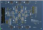
Figure 3-1 through Figure 3-5 illustrate the printed-circuit board (PCB) layouts.
Figure 3-1. Component Placement (Top Layer)
4
TPS65400 Buck Converter Evaluation Module User's Guide
Copyright © 2022 Texas Instruments Incorporated
SLVUAC4A – OCTOBER 2014 – REVISED MAY 2021
Submit Document Feedback
�www.ti.com
Board Layout
Figure 3-2. Board Layout (Top Layer)
Figure 3-3. Board Layout (Second Layer)
SLVUAC4A – OCTOBER 2014 – REVISED MAY 2021
Submit Document Feedback
TPS65400 Buck Converter Evaluation Module User's Guide
Copyright © 2022 Texas Instruments Incorporated
5
�Board Layout
www.ti.com
Figure 3-4. Board Layout (Third Layer)
Figure 3-5. Board Layout (Bottom Layer)
6
TPS65400 Buck Converter Evaluation Module User's Guide
Copyright © 2022 Texas Instruments Incorporated
SLVUAC4A – OCTOBER 2014 – REVISED MAY 2021
Submit Document Feedback
�www.ti.com
Bench Test Setup Conditions
4 Bench Test Setup Conditions
4.1 Headers Description and Jumper Placement
Figure 4-1 illustrates the header descriptions and jumper placement on the EVM.
Figure 4-1. Headers Description and Jumper Placement
Test points:
1.
2.
3.
4.
LX of VOUT1
LX of VOUT2
LX of VOUT3
LX of VOUT4
VOUT1, VOUT2, VOUT3, VOUT4
SLVUAC4A – OCTOBER 2014 – REVISED MAY 2021
Submit Document Feedback
TPS65400 Buck Converter Evaluation Module User's Guide
Copyright © 2022 Texas Instruments Incorporated
7
�Bench Test Setup Conditions
www.ti.com
Table 4-1. Input/Output Connection
No.
Function
Description
J2
Buck1 Connector
Output of Buck1
J5
Buck2 Connector
Output of Buck2
J7
Buck3 Connector
Output of Buck3
J9
Buck4 Connector
Output of Buck4
J6
Buck1/2/3/4 VIN Connector
Apply power supply to this connector
J13
PMBus/I2C Interface connector
Communication via PMBus/I2C Interface
Table 4-2. Jumpers
No.
Functions
Description
JP1-PVIN34-Vin-PVIN12
Short VIN to PVIN34
Vin tied to PVIN34
JP3-PVIN12-PVIN34
Short PVIN12 with PVIN34
PVIN34 tied to PVIN12
JP10-3-4
Connect Cap to SS1
tied SS1 to C40
JP10-7-8
Connect Cap to SS2
tied SS2 to C42
JP10-11-12
Connect Cap to SS3
tied SS3 to C43
JP10-15-16
Connect Cap to SS4
tied SS4 to C44
4.2 Hardware Requirement
This EVM requires an external power supply capable of providing 4.5 V to 18 V at 6 A.
The EVM kit includes USB2ANY interface box which, when installed on a PC and connected to the EVM, permits
communication with the EVM via a GUI interface. The minimum PC requirements are:
•
•
•
•
Microsoft® Windows® 2000, Windows XP, or Windows 7 operating system
USB port
Minimum of 30MB of free hard disk space (100MB recommended)
Minimum of 256MB of RAM
4.3 Hardware Setup
After connecting the power supply to J6 and turning on the power supply, the EVM regulates the output voltages
to the value listed in Table 1-1. Additional input capacitance may be required in order to mitigate the inductive
voltage droop that may occur during a load transient event.
In order to change the output voltage by sending the digital control signal via a PC running the TPS65400
controller software and USB2ANY interface box, perform the following steps:
1. Connect the USB port of USB2ANY to the PC using the USB cable and the other end to J13 of the
TPS65400 using the supplied 30-pin ribbon cable (Figure 4-2). The connectors on the ribbon cable are
keyed to prevent incorrect installation.
2. Connect the power supply on J6 and turn on the power supply.
3. Run the software as explained in Section 4.4.
8
TPS65400 Buck Converter Evaluation Module User's Guide
Copyright © 2022 Texas Instruments Incorporated
SLVUAC4A – OCTOBER 2014 – REVISED MAY 2021
Submit Document Feedback
�www.ti.com
Bench Test Setup Conditions
Figure 4-2. USB Interface Adapter Quick Connection Diagram
4.4 Software Install
If installing from the TI Web site, go to the URL, www.ti.com
Note
This installation page is best viewed with the Microsoft® Internet Explorer® browser and may not work
correctly with other browsers.
Click on the install button; the PC should give a security warning asking if you want to install this application.
Select Install to proceed. If a pre-release or Beta version is currently installed on the PC, uninstall this version of
the software before installing the final version.
The software attempts to install the Microsoft® .NET Framework 2.0 (if it is not already installed). This framework
is required for the software to run.
To run the software after installation, go to
Start → All programs → Texas Instruments → PI-Commander-0.8.4-672M → PI-Commander-PMU.
At start-up, the software first checks the firmware version of the USB2ANY adapter box. If an incorrect firmware
version is installed, the software automatically searches on the Internet (if connected) for updates. If a new
update is available, the software notifies the user of the update, and downloads and installs the software. Note
that after the firmware is updated, the USB cable between the adapter and PC must be disconnected and then
reconnected, as instructed during the install process. The host PC software also automatically searches on the
Internet (if connected) for updates. If a new update is available, the software notifies the user of the update and
downloads and installs it. During future use of the software, it may prompt you to install a new version if one
becomes available on the Web.
Note
VeriSign® Code Signing is used to prevent any malicious code from changing this application. If at any
time in the future the binaries are modified, the code will no longer attempt to run.
SLVUAC4A – OCTOBER 2014 – REVISED MAY 2021
Submit Document Feedback
TPS65400 Buck Converter Evaluation Module User's Guide
Copyright © 2022 Texas Instruments Incorporated
9
�Bench Test Setup Conditions
www.ti.com
4.5 Software Operation
This section provides descriptions of the EVM software.
The supplied software is used to communicate with the TPS65400 EVM. Click on the icon on the host computer
to start the software. The software displays the main control panel to connect with the EVM board.
1. Click on Rescan Slaves
2. Click on LM26430-00F1 6a
3. Click the No button on the popup dialog
Figure 4-3. Connect to TPS65400 EVM with EVM GUI
4. Click on PMBus Register Page
Figure 4-4. Go to Main Setting Panel
10
TPS65400 Buck Converter Evaluation Module User's Guide
Copyright © 2022 Texas Instruments Incorporated
SLVUAC4A – OCTOBER 2014 – REVISED MAY 2021
Submit Document Feedback
�www.ti.com
Bench Test Setup Conditions
Then, a detail setting panel is presented as shown in Figure 4-5.
Figure 4-5. Global Commands
Figure 4-6. Status and Main Setting Panel
SLVUAC4A – OCTOBER 2014 – REVISED MAY 2021
Submit Document Feedback
TPS65400 Buck Converter Evaluation Module User's Guide
Copyright © 2022 Texas Instruments Incorporated
11
�Bench Test Setup Conditions
www.ti.com
Figure 4-4 to Figure 4-9 show the control GUI interface. Vout voltage, phase shift, and power sequence are
programmed with this GUI. Detailed information for each option is in the datasheet. Reference the datasheet and
select the right option for your application (http://www.ti.com/products/tps65400).
One option is to Apply Changes Immediately; if this checkbox is selected, any change is immediately sent to the
EVM. STORE_DEFAULT_ALL must be clicked to write all settings to EEPROM. EEPROM values can be read
back from the EVM by clicking SOFT_RESET on Page 0xFF – ALL.
Figure 4-7. Phase Shift Panel
12
TPS65400 Buck Converter Evaluation Module User's Guide
Copyright © 2022 Texas Instruments Incorporated
SLVUAC4A – OCTOBER 2014 – REVISED MAY 2021
Submit Document Feedback
�www.ti.com
Bench Test Setup Conditions
Figure 4-8. Power Sequence Panel
Figure 4-9. Vref Ramping Up and Down Panel
SLVUAC4A – OCTOBER 2014 – REVISED MAY 2021
Submit Document Feedback
TPS65400 Buck Converter Evaluation Module User's Guide
Copyright © 2022 Texas Instruments Incorporated
13
�Power-Up Procedure
www.ti.com
5 Power-Up Procedure
1. Connect the USB2ANY adaptor to J13 on the EVM board and connect the other port from USB2ANY to the
USB port on the host computer
2. Apply 12 V to J6
3. Open the GUI on computer
14
TPS65400 Buck Converter Evaluation Module User's Guide
Copyright © 2022 Texas Instruments Incorporated
SLVUAC4A – OCTOBER 2014 – REVISED MAY 2021
Submit Document Feedback
�www.ti.com
Power-Down Procedure
6 Power-Down Procedure
1. Close the GUI on computer
2. Remove or shutdown 12 V on J6
3. Remove USB2ANY
SLVUAC4A – OCTOBER 2014 – REVISED MAY 2021
Submit Document Feedback
TPS65400 Buck Converter Evaluation Module User's Guide
Copyright © 2022 Texas Instruments Incorporated
15
�Bill of Materials
www.ti.com
7 Bill of Materials
Table 7-1 lists the bill of materials (BOM) for this EVM.
Table 7-1. Bill of Materials
Designator
Qty.
Value
Description
Package Reference
Part Number
Manufacturer
PWR678
Any
805
LMK212B7475KG-T
Taiyo Yuden
CAP, CERM, 1 µF, 25 V, ±10%, X7R, 0603_950
0603_950
C0603C105K3RACTU
Kemet
0.1 µF
CAP, CERM, 0.1 µF, 25 V, ±10%, X5R, 0603
603
06033D104KAT2A
AVX
1
10 µF
CAP, CERM, 10 µF, 10 V, ±10%, X5R, 0805
805
C0805C106K8PACTU
Kemet
C5
1
3.3 µF
CAP, CERM, 3.3 µF, 10 V, ±10%, X7R, 0805
805
GRM21BR71A335KA99L
Murata
C6, C32
2
22 µF
CAP, CERM, 22 µF, 25 V, ±20%, X5R, 1210
1210
12103D226MAT2A
AVX
C7, C8, C15, C16, C23,
C24, C33, C34
8
0.1 µF
CAP, CERM, 0.1µF, 25V, ±10%, X7R, 0603
603
GRM188R71E104KA01D
Murata
C9, C10, C17, C18,
C25, C26, C35, C36
8
22 µF
CAP, CERM, 22µF, 10V, ±10%, X7R, 1206
1206
GRM31CR71A226KE15L
Murata
C11
1
120 pF
CAP, CERM, 120 pF, 50 V, ±5%, C0G/NP0, 0603
603
06035A121JAT2A
AVX
C12, C20, C29, C38
4
22 pF
CAP, CERM, 22 pF, 50 V, ±5%, C0G/NP0, 0603
603
06035A220JAT2A
AVX
C13, C21, C30, C39
4
1000 pF
CAP, CERM, 1000 pF, 50 V, ±10%, C0G/NP0, 0603
603
06035A102KAT2A
AVX
C14, C22, C31, C41
4
4700 pF
CAP, CERM, 4700 pF, 50 V, ±10%, X5R, 0603
603
GRM188R61H472KA01D
Murata
C19
1
160 pF
CAP, CERM, 160 pF, 50 V, ±5%, C0G/NP0, 0603
603
GRM1885C1H161JA01D
Murata
C27, C37
2
68 pF
CAP, CERM, 68 pF, 50 V, ±5%, C0G/NP0, 0603
603
06035A680JAT2A
AVX
C28
1
0.1 µF
CAP, CERM, 0.1 µF, 50 V, ±10%, X7R, 0603
603
06035C104KAT2A
AVX
C40, C42, C43, C44
4
4700 pF
CAP, CERM, 4700 pF, 100 V, ±10%, X7R, 0603
603
06031C472KAT2A
AVX
C45
1
100 pF
CAP, CERM, 100 pF, 25 V, ±10%, X7R, 0603
603
06033C101KAT2A
AVX
C46
1
4.7 pF
CAP, CERM, 4.7 pF, 50 V, ±5%, C0G/NP0, 0603
603
06035A4R7CAT2A
AVX
H1, H2, H3, H4
4
Bumpon, Hemisphere, 0.44 X 0.20, Clear
Transparent Bumpon
SJ-5303 (CLEAR)
3M
J1, J16
2
Header, TH, 100mil, 3x1, Gold plated, 230 mil above insulator
TSW-103-07-G-S
TSW-103-07-G-S
Samtec, Inc.
J2, J4, J5, J6, J7, J9
6
Terminal Block, 6A, 3.5mm Pitch, 2-Pos, TH
7.0x8.2x6.5mm
ED555/2DS
On-Shore
Technology
J3, J11, J12, J14, J15
5
Header, TH, 100mil, 2x1, Gold plated, 230 mil above insulator
TSW-102-07-G-S
TSW-102-07-G-S
Samtec, Inc.
J8
1
Header, 100mil, 4x2, Gold, TH
4x2 Header
TSW-104-07-G-D
Samtec
J10
1
Header, 100mil, 8x2, Gold, TH
8x2 Header
TSW-108-07-G-D
Samtec
J13
1
Connector, 15x2, 3A 300V STRT DIP, TH
Connector, 15x2, Pitch 2.54mm, TH
XG4C-3031
Omron Electronic
Components
L1, L2, L3, L4
4
2.2µH
Inductor, Shielded, Composite, 2.2µH, 12.7A, 0.012 Ω, SMD
IND_6.4x3.1x6.6
XAL6030-222MEB
Coilcraft
R1, R6, R11, R16
4
0
RES, 0, 5%, 0.1 W, 0603
603
CRCW06030000Z0EA
Vishay-Dale
R2
1
49.9
RES, 49.9, 1%, 0.1 W, 0603
603
CRCW060349R9FKEA
Vishay-Dale
R3
1
12.7k
RES, 12.7 k, 1%, 0.1 W, 0603
603
CRCW060312K7FKEA
Vishay-Dale
R4, R9, R14, R20
4
15.4k
RES, 15.4 k, 1%, 0.1 W, 0603
603
CRCW060315K4FKEA
Vishay-Dale
PCB1
1
C1
1
4.7 µF
CAP, CERM, 4.7 µF, 10 V, ±10%, X7R, 0805
C2
1
1 µF
C3
1
C4
16
Printed Circuit Board
TPS65400 Buck Converter Evaluation Module User's Guide
SLVUAC4A – OCTOBER 2014 – REVISED MAY 2021
Submit Document Feedback
Copyright © 2022 Texas Instruments Incorporated
�www.ti.com
Bill of Materials
Table 7-1. Bill of Materials (continued)
Designator
Qty.
Value
Description
Package Reference
Part Number
Manufacturer
R5
1
10.2k
RES, 10.2 k, 1%, 0.1 W, 0603
603
CRCW060310K2FKEA
Vishay-Dale
R7
1
100
RES, 100, 1%, 0.1 W, 0603
603
CRCW0603100RFKEA
Vishay-Dale
R8
1
9.31k
RES, 9.31 k, 1%, 0.1 W, 0603
603
CRCW06039K31FKEA
Vishay-Dale
R10
1
3.01k
RES, 3.01 k, 1%, 0.1 W, 0603
603
CRCW06033K01FKEA
Vishay-Dale
R12
1
71.5
RES, 71.5, 1%, 0.1 W, 0603
603
CRCW060371R5FKEA
Vishay-Dale
R13
1
21.5k
RES, 21.5 k, 1%, 0.1 W, 0603
603
CRCW060321K5FKEA
Vishay-Dale
R15
1
43.2k
RES, 43.2 k, 1%, 0.1 W, 0603
603
CRCW060343K2FKEA
Vishay-Dale
R17
1
200
RES, 200, 1%, 0.1 W, 0603
603
CRCW0603200RFKEA
Vishay-Dale
R18, R27
2
22.1k
RES, 22.1 k, 1%, 0.1 W, 0603
603
CRCW060322K1FKEA
Vishay-Dale
R19, R22, R23, R24,
R25, R26, R31
7
10.0k
RES, 10.0 k, 1%, 0.1 W, 0603
603
CRCW060310K0FKEA
Vishay-Dale
R21
1
10.5k
RES, 10.5 k, 1%, 0.1 W, 0603
603
CRCW060310K5FKEA
Vishay-Dale
R28, R32, R33, R34,
R36, R37
6
1.0k
RES, 1.0 k, 5%, 0.1 W, 0603
603
CRCW06031K00JNEA
Vishay-Dale
R29, R30
2
3.0k
RES, 3.0 k, 5%, 0.1 W, 0603
603
CRCW06033K00JNEA
Vishay-Dale
R35
1
374k
RES, 374 k, 1%, 0.1 W, 0603
603
CRCW0603374KFKEA
Vishay-Dale
R38, R39, R40, R41
4
324k
RES, 324 k, 1%, 0.1 W, 0603
603
CRCW0603324KFKEA
Vishay-Dale
SH-JP1, SH-JP2, SHJP3, SH-JP4, SH-JP5,
SH-JP6
6
1x2
Shunt, 100mil, Gold plated, Black
Shunt
969102-0000-DA
3M
TP1, TP2, TP3, TP4,
TP5, TP6, TP7, TP8,
TP9, TP10, TP11, TP12
12
White
Test Point, Miniature, White, TH
White Miniature Testpoint
5002
Keystone
TP13, TP14, TP15,
TP16, TP17, TP18,
TP19, TP20, TP21,
TP22, TP23
11
Black
Test Point, Miniature, Black, TH
Black Miniature Testpoint
5001
Keystone
U1
1
4.5V to 18V Input Flexible Power Management Unit with PMBus/ I2C and RGZ0048G
Integrated Sequencing, RGZ0048G
TPS65400RGZ
or LM26430RGZ
Texas Instruments
FID1, FID2, FID3
0
Fiducial mark. There is nothing to buy or mount.
N/A
N/A
Fiducial
SLVUAC4A – OCTOBER 2014 – REVISED MAY 2021
Submit Document Feedback
TPS65400 Buck Converter Evaluation Module User's Guide
Copyright © 2022 Texas Instruments Incorporated
17
�Revision History
www.ti.com
8 Revision History
NOTE: Page numbers for previous revisions may differ from page numbers in the current version.
Changes from Revision * (October 2014) to Revision A (May 2021)
Page
• Updated user's guide title................................................................................................................................... 2
• Updated the numbering format for tables, figures, and cross-references throughout the document..................2
18
TPS65400 Buck Converter Evaluation Module User's Guide
Copyright © 2022 Texas Instruments Incorporated
SLVUAC4A – OCTOBER 2014 – REVISED MAY 2021
Submit Document Feedback
�IMPORTANT NOTICE AND DISCLAIMER
TI PROVIDES TECHNICAL AND RELIABILITY DATA (INCLUDING DATA SHEETS), DESIGN RESOURCES (INCLUDING REFERENCE
DESIGNS), APPLICATION OR OTHER DESIGN ADVICE, WEB TOOLS, SAFETY INFORMATION, AND OTHER RESOURCES “AS IS”
AND WITH ALL FAULTS, AND DISCLAIMS ALL WARRANTIES, EXPRESS AND IMPLIED, INCLUDING WITHOUT LIMITATION ANY
IMPLIED WARRANTIES OF MERCHANTABILITY, FITNESS FOR A PARTICULAR PURPOSE OR NON-INFRINGEMENT OF THIRD
PARTY INTELLECTUAL PROPERTY RIGHTS.
These resources are intended for skilled developers designing with TI products. You are solely responsible for (1) selecting the appropriate
TI products for your application, (2) designing, validating and testing your application, and (3) ensuring your application meets applicable
standards, and any other safety, security, regulatory or other requirements.
These resources are subject to change without notice. TI grants you permission to use these resources only for development of an
application that uses the TI products described in the resource. Other reproduction and display of these resources is prohibited. No license
is granted to any other TI intellectual property right or to any third party intellectual property right. TI disclaims responsibility for, and you
will fully indemnify TI and its representatives against, any claims, damages, costs, losses, and liabilities arising out of your use of these
resources.
TI’s products are provided subject to TI’s Terms of Sale or other applicable terms available either on ti.com or provided in conjunction with
such TI products. TI’s provision of these resources does not expand or otherwise alter TI’s applicable warranties or warranty disclaimers for
TI products.
TI objects to and rejects any additional or different terms you may have proposed. IMPORTANT NOTICE
Mailing Address: Texas Instruments, Post Office Box 655303, Dallas, Texas 75265
Copyright © 2022, Texas Instruments Incorporated
�