TPS65510
www.ti.com .......................................................................................................................................................................................... SLLS917 – SEPTEMBER 2008
LOW-POWER BATTERY BACKUP IC
WITH INTEGRATED BOOST CONVERTER
FEATURES
1
• Power-Path Switch to Select Main Battery or
Backup Battery for Real-Time Clock (RTC)
• Integrated Boost DC/DC Converter
– Modulation Select by Control Pin (PWMON),
Pulse Frequency Modulation (PFM) or
Pulse Width Modulation (PWM)
– Fixed Switching Frequency (PWM, 750 kHz)
– Peak Current Mode Control (PWM)
– Low Power Consumption (PFM)
• Four Integrated Low Dropout (LDO) Voltage
Regulators for 1.2 V/1.8 V/3.3 V
• Two Integrated Indicators
– CS: Monitors the Voltage Level of Main
Battery (VBAT) and Output voltage level of
Boost Converter (VO_BT)
– XRESET: Monitors the Output voltage Level
of 3.3V LDO (VOUT)
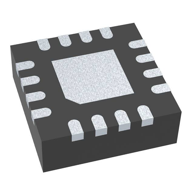
• 16-Pin QFN (3mm × 3mm) Package
• Operating Temperature –35°C to 85°C
• Protection
– Overcurrent Protection (OCP)
– Overvoltage Protection (OVP)
– Thermal Shutdown (TSD)
– Undervoltage Lockout (UVLO)
2
DESCRIPTION
The TPS65510 offers a suitable solution for power
switch to select the main battery or the backup
battery.
This device automatically selects the power path. It
depends on the voltage level of the VO_BT pin.
When the main battery is removed, the power path of
the VOUT pin is automatically changed from the
output of 3.3-V low droppout (LDO) voltage regulator
to the backup battery.
The backup battery is charged from the power path of
the VRO pin (output of 3.3-V LDO) via an external
diode and resistor. The input of the LDO voltage
regulator comes from the internal boost converter.
The 1.2-V output LDO and 1.8-V output LDO voltage
regulators have a enable pin, V_CTRL. If these
outputs are not necessary, V_CTRL should be
connected to AGND to save power consumption. The
self-power consumption is less than 3 µA (maximum)
using the backup battery.
This device has two indicators. One is CS, which
monitors the voltage level of the VBAT pin and
VO_BT pin. The other is XRESET, which monitors
voltage level of the VOUT pin. These indicators
should be connected to CPU/DSP to reset them.
This device reduces the total solution area and
extends the lifetime of the backup battery.
APPLICATIONS
•
•
Digital Still Cameras
Portable Systems With Backup Battery
1
2
Please be aware that an important notice concerning availability, standard warranty, and use in critical applications of Texas
Instruments semiconductor products and disclaimers thereto appears at the end of this data sheet.
PowerPAD is a trademark of Texas Instruments.
PRODUCTION DATA information is current as of publication date.
Products conform to specifications per the terms of the Texas
Instruments standard warranty. Production processing does not
necessarily include testing of all parameters.
Copyright © 2008, Texas Instruments Incorporated
�TPS65510
SLLS917 – SEPTEMBER 2008 .......................................................................................................................................................................................... www.ti.com
These devices have limited built-in ESD protection. The leads should be shorted together or the device placed in conductive foam
during storage or handling to prevent electrostatic damage to the MOS gates.
APPLICATION CIRCUIT
Figure 1. Typical Application Circuit (1.2-V/1.8-V Output)
Figure 2. Typical Application Circuit (3.3-V Output)
2
Submit Documentation Feedback
Copyright © 2008, Texas Instruments Incorporated
Product Folder Link(s): TPS65510
�TPS65510
www.ti.com .......................................................................................................................................................................................... SLLS917 – SEPTEMBER 2008
ORDERING INFORMATION
TA
PACKAGE MARKING
–35°C to 85°C
CGK
PACKAGE
16-pin QFN
PART NUMBER
TPS65510RGT
ABSOLUTE MAXIMUM RATINGS (1)
over operating free-air temperature range (unless otherwise noted)
MIN
MAX
VBAT, VBK
–0.3
6
SW
–0.3
7
–0.3
6
PWMON,
V_CTRL
–0.3
6
XRESET, CS
–0.3
6
–0.3
3.6
Input voltage range
FB, FBG
VRO, VOUT,
VO1R8, VO1R2
Output voltage range
VO_BT
SW
–0.3
Switch current
Maximum junction temperature range
Storage temperature range
(1)
–40
UNIT
V
V
6
V
1.3
A
125
°C
150
°C
Stresses beyond those listed under "absolute maximum ratings" may cause permanent damage to the device. These are stress ratings
only and functional operation of the device at these or any other conditions beyond those indicated under "recommended operating
conditions" is not implied. Exposure to absolute-maximum-rated conditions for extended periods may affect device reliability.
DISSIPATION RATINGS
(1)
PACKAGE
RθJA (1)
POWER RATING
TA < 25°C
POWER RATING
TA = 85°C
QFN
47.4°C/W
2.11 W
0.844 W
The thermal resistance, RθJA, is based on a soldered PowerPAD™ on 2S2P JEDEC board using thermal vias.
RECOMMENDED OPERATING CONDITIONS
over operating free-air temperature range (unless otherwise noted)
MIN
VBAT
VBK
VIH
VIL
Supply voltage
TYP
MAX
2.65
5.5
1.8
5.5
High-level digital input voltage at PWMON
1.4
5.5
High-level digital input voltage at V_CTRL
1.4
VOUT
Low-level digital input voltage at PWMON
0.4
Low-level digital input voltage at V_CTRL
0.4
Operating free-air temperature range
–35
85
Submit Documentation Feedback
Copyright © 2008, Texas Instruments Incorporated
Product Folder Link(s): TPS65510
UNIT
V
V
V
°C
3
�TPS65510
SLLS917 – SEPTEMBER 2008 .......................................................................................................................................................................................... www.ti.com
ELECTRICAL CHARACTERISTICS
TA = 25°C (unless otherwise noted)
PARAMETER
TEST CONDITIONS
MIN
TYP
MAX
UNIT
60
100
µA
ICC1
Consumption current at VO_BT
V(VO_BT): 3.6 V, VOUT: No load
V(PWMON): AGND (PFM mode)
ICC2
Consumption current at VO_BT
V(VO_BT): 5 V, VOUT: No load
V(PWMON): VOUT (PWM mode)
250
350
µA
ICC3
Consumption current at VBK
V(VO_BT) : 3.6 V, V(VBK): 3 V
VOUT: No load
0.1
1
µA
ICC4
Consumption current at VBK
VO_BT: Open, V(VBK): 3 V
VOUT: No load, V(V_CTRL): VOUT
2.5
5
µA
ICC5
Consumption current at VBK
VO_BT: Open, V(VBK): 3 V
VOUT: No load, V(V_CTRL): AGND
1.2
3
µA
ICC6
Consumption current at VBAT
V(VBAT): 3.6 V, V(VO_BT): 3.5 V
5
10
I(SINK_CS)
Sink current at CS
V(CS): 0.5 V, CS pin: Low-Z
I(LEAK_CS)
Leakage current at CS
V(CS): 5.5 V, CS pin: Hi-Z
I(SINK_XRESE
Sink current at XRESET
V(XRESET): 0.5 V, XRESET pin: Low-Z
Leak current at XRESET
V(XRESET): 5.5 V, XRESET pin: Hi-Z
1
µA
I(LEAK_VBK)
Leak current at VBK
V(VO_BT): 5.5 V, V(VBK): 0 V
1
µA
V(UVLO_DET)
UVLO/CS detection level at
VBAT
V(VBAT): from 0 V to 5.5 V
2.90
V
V(UVLO_HYS)
UVLO/CS hysteresis at VBAT
V(VBAT): from 5.5 V to 0 V
–250
–200
–150
mV
V(CS_DET)
CS detection level at VO_BT
V(VO_BT): from 5 V to 0 V
3.071
3.150
3.229
V(CS_HYS)
CS hysteresis at VO_BT
V(VO_BT): from 0 V to 5 V
50
100
150
V(XRESET_DE
XRESET detection level
V(VOUT): from 3.3 V to 0 V
2.048
2.100
2.153
XRESET hysteresis
V(VOUT): from 0 V to 3.3 V
50
100
150
mV
V(SW1)
Change the power path for
VOUT
Monitoring at VO_BT
2.94
3.00
3.06
V
V(SW2)
CS output disable level
Monitoring at VOUT
3.072
3.135
3.198
V
T)
I(LEAK_XRESE
T)
T)
V(XRESET_HY
S)
1
1.5
1
1
2.50
1.5
2.70
µA
mA
µA
mA
V
mV
V
V(WAKE_DET) Threshold of WAKE mode
V(VO_BT): from 0 V to 3.6 V
2.38
2.50
2.63
V
V(WAKE_HYS) WAKE mode hysteresis
V(VO_BT): from 3.6 V to 0 V
–150
–100
–50
mV
30
60
Ω
R(ON_VBK)
On resistance between VBK and
VOUT
TSD (1)
Thermal shutdown detection
temperature
(1)
4
VO_BT: Open, V(VBK): 3 V,
I(VOUT): 2 mA
150
°C
Specified by design. Not production tested.
Submit Documentation Feedback
Copyright © 2008, Texas Instruments Incorporated
Product Folder Link(s): TPS65510
�TPS65510
www.ti.com .......................................................................................................................................................................................... SLLS917 – SEPTEMBER 2008
ELECTRICAL CHARACTERISTICS (continued)
TA = 25°C (unless otherwise noted)
PARAMETER
TEST CONDITIONS
MIN
TYP
MAX
V(PWMON): AGND (PFM mode)
1.213
1.250
1.288
V(PWMON): VOUT (PWM mode)
1.225
1.250
1.275
Monitoring at FB
1.30
1.35
1.40
V(PWMON): AGND (PFM mode)
0.48
0.60
0.72
V(PWMON): VOUT (PWM mode)
0.8
1.0
1.2
675
UNIT
Boost DC/DC Converter
V(FB)
Reference voltage
Overvoltage protection threshold
Overcurrent protection threshold
V
V
A
OSC
Internal OSC frequency
V(PWMON): VOUT (PWM mode)
750
825
kHz
R(ON_P)
P-ch FET ON resistance
V(VO_BT): 5 V
500
700
mΩ
R(ON_N)
N-ch FET ON resistance
V(VO_BT): 5 V
200
250
mΩ
R(ON_FBG)
FBG ON resistance
V(PWMON): VOUT (PWM mode)
1
1.5
kΩ
I(LEAK_FBG)
Leakage current at FBG
V(PWMON): AGND (PFM mode)
1
µA
3.3-V Output LDO (VOUT)
V(VOUT)
Output voltage of VOUT
V(VO_BT): 5 V, I(VOUT): 1 mA
I(VOUT)
Output current of VOUT
V(VO_BT): 5 V, V(VOUT) ≥ 3.156 V
3.234
3.300
3.366
30
Overcurrent protection threshold
50
V
mA
mA
3.3-V Output LDO (VRO)
V(VRO)
Output voltage of VRO
V(VO_BT): 5 V, I(VRO): 1 mA
I(VRO)
Output current of VRO
V(VO_BT): 5 V, V(VRO) ≥ 3.156 V
3.234
3.300
3.366
10
30
Overcurrent protection threshold
50
V
mA
mA
1.8-V Output LDO (VO1R8)
V(VO1R8)
Output voltage of VO1R8
V(V_CTRL): VOUT, V(VO_BT): 5 V, I(VO1R8): 100 µA
I(VO1R8)
Output current of VO1R8
V(V_CTRL): VOUT
1.71
1.80
1.89
V
100
µA
1.2-V Output LDO (VO1R2)
V(VO1R2)
Output voltage of VO1R2
V(V_CTRL): VOUT, V(VO_BT): 5 V, I(VO1R2): 100 µA
I(VO1R2)
Output current of VO1R2
V(V_CTRL): VOUT
1.1
1.2
1.3
V
100
µA
SWITCHING CHARACTERISTICS
TA = 25°C (unless otherwise noted)
PARAMETER
TCS
(1)
TXRESET (1)
(1)
TEST CONDITIONS
MIN
TYP
MAX
UNIT
Detection delay at CS
V(VO_BT): from 3.6 V to 2.0 V
55
µs
Detection delay at XRESET
V(VOUT): from 1.5 V to 3.0 V
25
µs
Specified by design. Not production tested.
Submit Documentation Feedback
Copyright © 2008, Texas Instruments Incorporated
Product Folder Link(s): TPS65510
5
�TPS65510
SLLS917 – SEPTEMBER 2008 .......................................................................................................................................................................................... www.ti.com
Figure 3. Block Diagram
6
Submit Documentation Feedback
Copyright © 2008, Texas Instruments Incorporated
Product Folder Link(s): TPS65510
�TPS65510
www.ti.com .......................................................................................................................................................................................... SLLS917 – SEPTEMBER 2008
PIN ASSIGNMENTS
TERMINAL FUNCTIONS
TERMINAL
(1)
I/O (1)
DESCRIPTION
NO.
NAME
1
VO_BT
O
Boost converter output. This voltage is defined by the ration of external resistors. Please see
the description in detail.
2
SW
I
Switching terminal for boost converter. This terminal should be connected to the external
inductor.
3
PGND
G
Power ground. Connect to the ground plane.
4
AGND
G
Analog ground. Connect to the ground lane.
5
V_CTRL
I
LDO Enable/Disable input. When the input level is Low, it disables the operation of LDOs
regarding VO1R8 and VO1R2. When the input level is high, it enables the operation of LDOs
regarding VO1R8 and VO1R2.
6
PWMON
I
Modulation select pin. When the input level is low, the boost converter operates as PFM
mode. When the input level is high, the boost converter operates as PWM mode.
7
CS
O
Indicator which monitors VBAT pin and VO_BT pin. CS is an open-drain output that goes low
when the voltage level of VO_BT pin or VBAT pin is lower than the threshold. The threshold
is specified with the Electrical Characteristics.
8
XRESET
O
Indicator that monitors VOUT; the output of 3.3-V LDO or backup battery. XRESET is an
open-drain output that goes low when the voltage level of VOUT is lower than the threshold.
The threshold is specified with the Electrical Characteristics.
9
VO1R2
O
1.2-V output regulated by LDO. The voltage level sets 1.2 V internally.
10
VO1R8
O
1.8-V output regulated by LDO. The voltage level sets 1.8 V internally.
11
VOUT
O
3.3-V output regulated by LDO or the voltage from backup battery. This output is selected by
internal power switch. The selection depends on the output voltage of boost converter.
12
VRO
O
3.3-V output regulated by LDO. The voltage level sets 3.3 V internally.
13
VBK
I
Backup battery input. The recommended input voltage at VBK is from 1.8V to 5.5V.
14
FBG
I
Boost converter output adjustable pin. When the level of PWMON pin is low, the impedance
of FBG is high impedance. When the level of PWMON pin is high, the impedance of FBG is
almost GND level.
15
FB
I
Feedback voltage from boost converter output.
16
VBAT
I
Power supply from main battery. The recommended input voltage at VBAT is from 2.65V to
5.5V.
I: Input pin, O: Output pin, P: Power supply pin, G: GND pin
Submit Documentation Feedback
Copyright © 2008, Texas Instruments Incorporated
Product Folder Link(s): TPS65510
7
�TPS65510
SLLS917 – SEPTEMBER 2008 .......................................................................................................................................................................................... www.ti.com
I/O Equivalent Circuits
8
VBAT/VO_BT
CS/XRESET
V_CTRL
PWMON
FB
FBG
SW
VOUT
Submit Documentation Feedback
Copyright © 2008, Texas Instruments Incorporated
Product Folder Link(s): TPS65510
�TPS65510
www.ti.com .......................................................................................................................................................................................... SLLS917 – SEPTEMBER 2008
I/O Equivalent Circuits (continued)
VO1R2
VO1R8
VBK
VRO
Figure 4. I/O Equivalent Circuits
Submit Documentation Feedback
Copyright © 2008, Texas Instruments Incorporated
Product Folder Link(s): TPS65510
9
�TPS65510
SLLS917 – SEPTEMBER 2008 .......................................................................................................................................................................................... www.ti.com
FUNCTIONAL DESCRIPTION
Power-Path Switch
The TPS65510 has the switch to select a power path of VOUT pin from main battery or backup battery. These
switches consist of P-ch MOSFET. Also, these switches avoid the reverse current from output side to battery
side.
When the voltage of VO_BT pin (output of boost converter) is higher than the threshold specified by V(SW1) in
Electrical Characteristics, the power path of VOUT comes from main battery via internal boost converter. The
voltage of VOUT pin sets 3.3 V with internal LDO.
When a voltage of VO_BT pin is lower than the threshold specified by V(SW1) in Electrical Characteristics, the
power path of VOUT comes from backup battery at VBK pin. Before the voltage of VO_BT pin reaches V(SW1),
the switch to select a power path cannot change the power path route.
The voltage coming from backup battery is not regulated internally. When the voltage of VOUT is lower than the
threshold specified by V (XRESET_DET) and V (XRESET_HYS) in Electrical Characteristics, the voltage of XRESET pin
goes low (see the description of STATUS INDICATORS).
At the start of boost converter operation, the power path is different to avoid the power supply from backup
battery. In this situation, the power path of VOUT comes from main battery via internal boost converter even if
the output voltage of VO_BT is lower than threshold for CS signal specified by V(sw1) in Electrical Characteristics.
Boost Converter
The TPS65510 has the boost converter, and the power path comes from the main battery. It has four operation
modes, WAKE mode, Pulse Frequency Modulation (PFM) mode, Pulse Width Modulation (PWM) mode and
THROUGH mode.
At first, this converter operates as WAKE mode until the voltage of VO_BT pin is less than the threshold
specified by V(WAKE_DET) and V(WAKE_HYS) in Electrical Characteristics. The switching frequency of WAKE mode is
fixed. Only N-ch MOSFET operates during WAKE mode until the voltage of VO_BT pin reaches the threshold
specified by V(WAKE_DET) and V(WAKE_HYS) in Electrical Characteristics.
After the voltage of VO_BT pin reaching more than the threshold specified by V(WAKE_DET) and V(WAKE_HYS) in
Electrical Characteristics, the operation mode is shifted from WAKE mode to other modes selected by the level of
PWMON pin. When the voltage of PWMON pin is low level, the boost converter operates as PFM mode. When
the voltage of PWMON pin is high level, the boost converter operates as PWM mode. When the voltage of main
battery is higher than the voltage of VO_BT pin, the converter operates as THROUGH mode to reduce the
consumption current at VO_BT pin. At this mode, The TPS65510 forces P-ch MOSFET to be ON and N-ch
MOSFET to be OFF. It means that the voltage of VO_BT pin is not regulated.
The boost converter has the reversed current protection to monitor the different voltage between VO_BT pin and
SW pin. The protection monitors the difference at both PFM mode and PWM mode. When the voltage of SW pin
is larger than that of VO_BT pin, the protection is activated. When the protection is activated, the internal P-ch
MOSFET turns OFF. This means that the voltage of SW pin converges the battery voltage naturally.
The output voltage of boost converter depends on the operation mode. When the boost converter operates as
PFM mode, the impedance of FBG pin goes Hi-Z and the output voltage is defined by R1, R2 and R3 shown in
Figure 1 and Figure 2. When the boost converter operates as PWM mode, the impedance of FBG pin goes
almost zero and the output voltage is defined by R1 and R2 shown in Figure 1 and Figure 2. The output voltage
is calculated by Equation 1 and Equation 2.
10
Submit Documentation Feedback
Copyright © 2008, Texas Instruments Incorporated
Product Folder Link(s): TPS65510
�TPS65510
www.ti.com .......................................................................................................................................................................................... SLLS917 – SEPTEMBER 2008
PFM mode:
R1 ö
æ
VVO_BT = ç1 +
÷ • VFB
R
2 + R3ø
è
(1)
PWM mode:
R1 ö
æ
VVO_BT = ç1 +
•VFB
R2 ÷ø
è
(2)
Where:
VVO_BT: Voltage of VO_BT pin
VFB: Voltage of FB
pin defined by
reference voltage in
Electrical
Characteristics
LDO Voltage Regulators
The TPS65510 has four types of LDO voltage regulators; 1.2-V output (LDO1, shown in Figure 3), 1.8-V output
(LDO2, shown in Figure 3) and 3.3-V dual output (LDO3 and LDO4, shown in Figure 3). These output voltage
are set by internal feedback loop only. The device has enable/disable control pin named V_CTRL for LDO1 and
LDO2. When the voltage of V_CTRL is low level, the device disables the output of LDO1 and LDO2. When the
voltage of V_CTRL is high level, the device enables the output of LDO1 and LDO2.
The power paths of LDO2, LDO3, and LDO4 are fixed; from output of LDO3 for LDO2 and from output of boost
converter for LDO3 and LDO4. The power path of LDO1 is selected by power path switch; when output voltage
of the boost converter is higher than the threshold specified by V(SW1) in Electrical Characteristics, the path
comes from output of LDO4. When output voltage of the boost converter is lower than the threshold specified by
V(SW1) in Electrical Characteristics, the path comes from backup battery connected to VBK pin.
The maximum outputs current are specified by I(VO1R2), I(VO1R8), I(VRO) and I(VOUT) in Electrical Characteristics.
Status Indicators
The TPS65510 has two device status indicators; CS and XRESET. These signal pins consist of open drain of
N-ch MOSFET. Due to this, the pullup resistors should be needed. The recommended values of pullup resistors
are 100 kΩ.
CS function monitors the voltage level of VBAT pin and VO_BT pin for selecting power path of VOUT. When the
signal level of CS pin is high level, the power path of VOUT comes from the main battery via the boost converter.
When the signal level of CS pin is low level, it comes from backup battery except the starting operation of boost
converter. When the boost converter starts operation with the main battery, the P-ch MOSFET at LDO4 turns ON
to avoid supplying the power from backup battery even if the voltage of VOUT is lower than the threshold
specified by V(SW1) in Electrical Characteristics. The signal of the CS pin remains low level when the main battery
is removed (including the transition) or the voltage level of VOUT does not achieve the threshold specified by
V(SW2) in Electrical Characteristics.
XRESET function monitors the voltage level of VOUT pin for resetting the load like RTC. When the voltage of
VOUT is more than the threshold specified by V(XRESET_DET) and V(XRESET_HYS) in Electrical Characteristics, the
signal level of XRESET pin is high. When the voltage of VOUT is less than the threshold specified by
V(XRESET_DET) and V(XRESET_HYS) in Electrical Characteristics, the signal level of XRESET pin is low. This situation
requires resetting the load. The detailed waveform is shown in Figure 5.
Submit Documentation Feedback
Copyright © 2008, Texas Instruments Incorporated
Product Folder Link(s): TPS65510
11
�TPS65510
SLLS917 – SEPTEMBER 2008 .......................................................................................................................................................................................... www.ti.com
Summary of Status Indicator and Power-Path Switch
Description
CS (1)
Disable
CS signal
XRESET
Power SW (2)
(1)
(2)
12
Detection
Voltage of VO_BT pin
Detect level
V(CS_DET) and V(CS_HYS) in Electrical Characteristics
Detection
Voltage of VOUT pin
Detect level
V(SW2) in Electrical Characteristics
Detection
Voltage of VOUT pin
Detect level
V(XRESET_DET) and V(XRESET_HYS) in Electrical Characteristics
Detection of
path change
Voltage of VO_BT pin
Detect level
V(SW1) in Electrical Characteristics
When the voltage of VBAT pin is less than the threshold of UVLO, the output of CS pin forces low level.
The Power path switch changes the path after the voltage of VO_BT is higher than V(CS_DET). Before that, the power path of VOUT
comes from VO_BT pin; not VBK pin.
Submit Documentation Feedback
Copyright © 2008, Texas Instruments Incorporated
Product Folder Link(s): TPS65510
�TPS65510
www.ti.com .......................................................................................................................................................................................... SLLS917 – SEPTEMBER 2008
Figure 5. Power-Path Switch Timing Chart
Submit Documentation Feedback
Copyright © 2008, Texas Instruments Incorporated
Product Folder Link(s): TPS65510
13
�TPS65510
SLLS917 – SEPTEMBER 2008 .......................................................................................................................................................................................... www.ti.com
Protection
The TPS65510 has over current protection (OCP), over voltage protection (OVP) Thermal shutdown (TSD) and
Under Voltage Lock Out (UVLO). See Table 1.
Table 1. Conditions of Protections
PIN
PROTECTION
OVP
SW
OCP
VOUT
VRO
-
VBAT
14
OCP
OCP
TSD
UVLO
CONDITION
Detect condition
Voltage of FB pin is greater than the threshold.
Change mode
Operation disable without latch off
Recovery condition
Voltage of FB pin is less than the threshold (auto recovery).
Detect condition
Current of SW pin is greater than the threshold with counting 64 cycles × 750 [kHz] and
the output voltage of VO_BT is less than 85% compared with the target voltage.
Change mode
Operation mode changes from PWM mode to PFM mode.
Recovery condition
Current of SW pin is less than the threshold and input edge signal from low level to high
level at the PWMON pin.
Detect condition
Current of VOUT pin is greater than the threshold.
Change mode
Operation disable without latch off
Recovery condition
Current of VOUT pin is less than the threshold (auto recovery).
Detect condition
Current of VRO pin is greater than the threshold.
Change mode
Operation disable without latch off
Recovery condition
Current of VRO pin is less than the threshold (auto recovery).
Detect condition
Temperature of chip is greater than the threshold.
Change mode
Operation of boost converter shuts down with latch off.
Recovery condition
Temperature of chip is lower than the threshold. Connect the main battery after
disconnecting the main battery from the system
Detect condition
Voltage of VBAT pin is less than the threshold.
Change mode
Operation of boost converter shutdown without latch off
Recovery condition
Connect the main battery after disconnecting the main battery from the system.
Submit Documentation Feedback
Copyright © 2008, Texas Instruments Incorporated
Product Folder Link(s): TPS65510
�PACKAGE OPTION ADDENDUM
www.ti.com
10-Dec-2020
PACKAGING INFORMATION
Orderable Device
Status
(1)
Package Type Package Pins Package
Drawing
Qty
Eco Plan
(2)
Lead finish/
Ball material
MSL Peak Temp
Op Temp (°C)
Device Marking
(3)
(4/5)
(6)
TPS65510RGTR
ACTIVE
VQFN
RGT
16
3000
RoHS & Green
NIPDAU
Level-2-260C-1 YEAR
-35 to 85
CGK
TPS65510RGTT
ACTIVE
VQFN
RGT
16
250
RoHS & Green
NIPDAU
Level-2-260C-1 YEAR
-35 to 85
CGK
(1)
The marketing status values are defined as follows:
ACTIVE: Product device recommended for new designs.
LIFEBUY: TI has announced that the device will be discontinued, and a lifetime-buy period is in effect.
NRND: Not recommended for new designs. Device is in production to support existing customers, but TI does not recommend using this part in a new design.
PREVIEW: Device has been announced but is not in production. Samples may or may not be available.
OBSOLETE: TI has discontinued the production of the device.
(2)
RoHS: TI defines "RoHS" to mean semiconductor products that are compliant with the current EU RoHS requirements for all 10 RoHS substances, including the requirement that RoHS substance
do not exceed 0.1% by weight in homogeneous materials. Where designed to be soldered at high temperatures, "RoHS" products are suitable for use in specified lead-free processes. TI may
reference these types of products as "Pb-Free".
RoHS Exempt: TI defines "RoHS Exempt" to mean products that contain lead but are compliant with EU RoHS pursuant to a specific EU RoHS exemption.
Green: TI defines "Green" to mean the content of Chlorine (Cl) and Bromine (Br) based flame retardants meet JS709B low halogen requirements of


 工商网监
湘ICP备2023018690号
工商网监
湘ICP备2023018690号
