www.ti.com
Table of Contents
User’s Guide
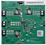
TPS65580 Buck Converter Evaluation Module User's
Guide
ABSTRACT
This user's guide contains information for the TPS65580 as well as support documentation for the
TPS65580EVM-575 evaluation module. Included are the performance specifications, board layouts, schematic,
and the bill of materials of the TPS65580EVM-575.
Table of Contents
1 Introduction.............................................................................................................................................................................2
2 Performance Specification Summary................................................................................................................................... 3
3 Modifications...........................................................................................................................................................................3
3.1 Output Voltage Setpoint..................................................................................................................................................... 3
4 Test Setup and Results.......................................................................................................................................................... 4
4.1 Input/Output Connections.................................................................................................................................................. 5
4.2 Start-Up Procedure............................................................................................................................................................ 5
4.3 Efficiency............................................................................................................................................................................6
4.4 Load Regulation................................................................................................................................................................. 9
4.5 Line Regulation.................................................................................................................................................................. 9
4.6 Load Transient Response................................................................................................................................................ 10
4.7 Input Voltage Ripple......................................................................................................................................................... 10
4.8 Start-Up............................................................................................................................................................................ 11
5 Board Layout.........................................................................................................................................................................12
5.1 Layout.............................................................................................................................................................................. 12
6 Schematic, Bill of Materials, and Reference...................................................................................................................... 14
6.1 Schematic........................................................................................................................................................................ 14
6.2 Bill of Materials.................................................................................................................................................................15
6.3 Reference.........................................................................................................................................................................16
7 Revision History................................................................................................................................................................... 16
Trademarks
D-CAP2™ is a trademark of Texas Instruments.
All trademarks are the property of their respective owners.
SLVU952B – SEPTEMBER 2013 – REVISED MAY 2021
TPS65580 Buck Converter Evaluation Module User's Guide
Submit Document Feedback
Copyright © 2022 Texas Instruments Incorporated
1
�Introduction
www.ti.com
1 Introduction
The TPS65580 is a triple output, advanced D-CAP2™-mode, synchronous buck converter requiring a very
low external component count. The advanced D-CAP2 control circuit is optimized for low-ESR output
capacitors such as POSCAP, SP-CAP, or ceramic types and features fast transient response with no external
compensation. The switching frequency is internally set at a nominal 700 kHz. The high-side and low-side
switching MOSFETs are incorporated inside the TPS65580 package along with the gate-drive circuitry. The low
drain-to-source on resistance of the MOSFETs allows the TPS65580 to achieve high efficiencies and helps keep
the junction temperature low at high output currents. The TPS65580 dc/dc synchronous converter is designed
to provide up to 1.5-A, 2.5-A and 1.5-A output for each of 3 channels from an input voltage source of 4.5 V to
18 V. The output voltage range is from 0.76 V to 6.5 V. Rated input voltage, output voltage and output current
ranges for the evaluation module are given in Table 1-1. This user’s guide describes the TPS65580EVM-575
performance.
Table 1-1. Input Voltage, Output Voltage and Output Current Summary
2
EVM
Input Voltage Range
Channel
Output Voltage
Output Current
Range
TPS65580EVM-575
VIN = 4.5 V to 18 V
CH1
3.3 V
0-A to 1.5-A
CH2
1.2 V
0-A to 2.5-A
CH3
1.5 V
0-A to 1.5-A
TPS65580 Buck Converter Evaluation Module User's Guide
SLVU952B – SEPTEMBER 2013 – REVISED MAY 2021
Submit Document Feedback
Copyright © 2022 Texas Instruments Incorporated
�www.ti.com
Performance Specification Summary
2 Performance Specification Summary
A summary of the TPS65580EVM-575 performance specifications is provided in Table 2-1. Specifications are
given for an input voltage of VIN = 12 V and Ta = 25°C unless otherwise noted.
Table 2-1. TPS65580EVM-575 Performance Specifications Summary
Specifications
Test Conditions
Input voltage range (VIN)
Min
Typ
Max
4.5
12
18
Operating frequency
Output voltage
CH1
Output current range
VIN = 12 V, LO = 3.3 µH
Output ripple voltage
VIN = 12 V, IO = 1.5 A
Output voltage
CH1
Output current range
VIN = 12 V, LO = 2.2 µH
Output ripple voltage
VIN = 12 V, IO = 2.5 A
Output voltage
CH1
kHz
3.3
V
1.5
Output current range
A
2.0
A
10
mVPP
1.2
V
0
Over current limit
V
700
0
Over current limit
Unit
2.5
A
3.5
A
10
mVPP
1.5
V
0
1.5
A
Over current limit
VIN = 12 V, LO = 2.2 µH
2.0
A
Output ripple voltage
VIN = 12 V, IO = 1.5 A
10
mVPP
3 Modifications
These evaluation modules are designed to provide access to the features of the TPS65580. Some modifications
can be made to this module.
3.1 Output Voltage Setpoint
To change the output voltage of the EVMs, it is necessary to change the value of the top resistor in the voltage
set point divider network (R9, R13, and R17). Changing the value of RTOP can change the output voltage above
0.765 V. The value of RTOP for a specific output voltage can be calculated using Equation 1.
æ V
ö
R TOP = RBOT × ç OUT -1÷
è 0.764V ø
(1)
Table 3-1 lists the RTOP values for some common output voltages. A feed-forward capacitor (CFF) may be
optionally used to improve phase margin. Pads for this component (C12, C18, and C24 ) are provided on
the printed-circuit board. Note that the values given in Table 3-1 are standard values and not the exact value
calculated using Equation 1.
Table 3-1. Output Voltages
LOUT
(µH)
Output Voltage
(V)
RTOP
(kΩ)
RBOT
(kΩ)
CFF
(pF)
COUT
(µF)
Min
Typ
Max
1.0
.681
2.21
220 - 680
1.5
2.2
3.3
22 - 68
1.05
.825
2.21
100 - 680
1.5
2.2
3.3
22 - 68
1.2
1.27
2.21
68 - 680
1.5
2.2
3.3
22 - 68
1.5
2.10
2.21
68 - 330
1.5
2.2
3.3
22 - 68
1.8
3.01
2.21
5 - 68
1.5
2.2
3.3
22 - 68
2.5
4.99
2.21
5 - 22
2.2
3.3
4.7
22 - 68
3.3
7.32
2.21
5 - 22
2.2
3.3
4.7
22 - 68
5.0
12.4
2.21
5 - 22
2.2
3.3
4.7
22 - 68
6.5
16.5
2.21
5 - 22
2.2
3.3
4.7
22 - 68
SLVU952B – SEPTEMBER 2013 – REVISED MAY 2021
TPS65580 Buck Converter Evaluation Module User's Guide
Submit Document Feedback
Copyright © 2022 Texas Instruments Incorporated
3
�Test Setup and Results
www.ti.com
4 Test Setup and Results
This section describes how to properly connect, set up, and use the TPS65580EVM-575. The section also
includes test results typical for the evaluation modules and efficiency, output load regulation, output line
regulation, load transient response, output voltage ripple, input voltage ripple, start-up, and switching frequency.
4
TPS65580 Buck Converter Evaluation Module User's Guide
SLVU952B – SEPTEMBER 2013 – REVISED MAY 2021
Submit Document Feedback
Copyright © 2022 Texas Instruments Incorporated
�www.ti.com
Test Setup and Results
4.1 Input/Output Connections
The TPS65580EVM-575 is provided with input/output connectors and test points as shown in Table 4-1. A power
supply capable of supplying 5 A must be connected to J1 through a pair of 20-AWG wires. The loads must be
connected to J2, J3 and J4 through pairs of 20-AWG wires. The maximum load current capability is for each
channel is shown in Table 1-1. Wire lengths must be minimized to reduce losses in the wires. Test point TP1
provides a place to monitor the VIN input voltages with TP2 providing a convenient ground reference. Test points
TP11, TP15 and TP19 are used to monitor the output voltage for each of the three channels. Test points TP12,
TP18 and TP20 are used as the ground reference for each of the three channels.
Table 4-1. Connections and Test Points
Reference Designator
Function
J1
VIN (see Table 1-1 for VIN range)
J2
CH1 VOUT, 3.3 V at 1.5-A maximum
J3
CH2 VOUT, 1.2 V at 2.5-A maximum
J4
CH3 VOUT, 1.5 V at 1.5-A maximum
JP1
CH1 EN control. Jumper JP1-2 to JP1-3 to disable, jumper JP1-2 to JP1-1 to enable.
JP2
CH2 EN control. Jumper JP2-2 to JP2-3 to disable, jumper JP2-2 to JP2-1 to enable.
JP3
CH3 EN control. Jumper JP3-2 to JP3-3 to disable, jumper JP3-2 to JP3-1 to enable.
TP1
VIN test point at VIN connector
TP2
GND test point at VIN
TP3
CH1 EN test point
TP4
CH2 EN test point
TP5
CH3 EN test point
TP6
Power good test point
TP7
Power ground test point
TP8
Analog ground test point
TP9
CH1 switch node test point
TP10
CH1 loop response test point
TP11
CH1 output voltage test point
TP12
CH1 ground test point at output connector
TP13
CH2 switch node test point
TP14
CH2 loop response test point
TP15
CH2 output voltage test point
TP16
CH2 ground test point at output connector
TP17
CH3 switch node test point
TP18
CH3 loop response test point
TP19
CH3 output voltage test point
TP20
CH3 ground test point at output connector
4.2 Start-Up Procedure
1. Ensure that the jumpers at JP1 (CH1 Enable control), JP2 (CH2 Enable control) and JP3 (CH3 Enable
control) is set from ON to OFF
2. Apply appropriate VIN voltage to VIN and GND terminals at J1
3. Set the jumpers at JP1 (CH1 Enable control), JP2 (CH2 Enable control) and JP3 (CH3 Enable control) to
ON. The EVM enables the output voltages for each of the three channels.
SLVU952B – SEPTEMBER 2013 – REVISED MAY 2021
TPS65580 Buck Converter Evaluation Module User's Guide
Submit Document Feedback
Copyright © 2022 Texas Instruments Incorporated
5
�Test Setup and Results
www.ti.com
4.3 Efficiency
Figure 4-1 shows the efficiency for the TPS65580EVM-575 CH1.
100
90
80
70
Efficiency - %
VIN = 5 V
VIN = 12 V
60
50
40
30
20
10
0
0.00
0.25
0.50
0.75
1.00
1.25
1.50
Output Current - A
C001
Figure 4-1. TPS65580EVM-575 CH1 Efficiency
Figure 4-2 shows the efficiency at light loads for the TPS65580EVM-575 CH1.
100
90
80
VIN = 5 V
Efficiency - %
70
60
50
VIN = 12 V
40
30
20
10
0
0.001
0.01
0.1
1
10
Output Current - A
C002
Figure 4-2. TPS65580EVM-575 Light CH1 Load Efficiency
6
TPS65580 Buck Converter Evaluation Module User's Guide
SLVU952B – SEPTEMBER 2013 – REVISED MAY 2021
Submit Document Feedback
Copyright © 2022 Texas Instruments Incorporated
�www.ti.com
Test Setup and Results
Figure 4-3 shows the efficiency for the TPS65580EVM-575 CH2.
100
90
80
Efficiency - %
70
60
VIN = 5 V
50
VIN = 12 V
40
30
20
10
0
0.00
0.25
0.50
0.75
1.00
1.25
1.50
1.75
2.00
Output Current - A
C001
Figure 4-3. TPS65580EVM-575 CH2 Efficiency
Figure 4-4 shows the efficiency at light loads for the TPS65580EVM-575 CH2.
100
90
80
Efficiency - %
70
VIN = 5 V
60
50
40
30
VIN = 12 V
20
10
0
0.001
0.01
0.1
1
10
Output Current - A
C002
Figure 4-4. TPS65580EVM-575 Light CH2 Load Efficiency
SLVU952B – SEPTEMBER 2013 – REVISED MAY 2021
TPS65580 Buck Converter Evaluation Module User's Guide
Submit Document Feedback
Copyright © 2022 Texas Instruments Incorporated
7
�Test Setup and Results
www.ti.com
Figure 4-5 shows the efficiency for the TPS65580EVM-575 CH3.
100
90
80
Efficiency - %
70
60
VIN = 5 V
VIN = 12 V
50
40
30
20
10
0
0.00
0.25
0.50
0.75
1.00
1.25
1.50
Output Current - A
C001
Figure 4-5. TPS65580EVM-575 CH3 Efficiency
Figure 4-6 shows the efficiency at light loads for the TPS65580EVM-575 CH3.
100
90
80
VIN = 5 V
Efficiency - %
70
60
50
VIN = 12 V
40
30
20
10
0
0.001
0.01
0.1
1
10
Output Current - A
C002
Figure 4-6. TPS65580EVM-575 Light CH3 Load Efficiency
8
TPS65580 Buck Converter Evaluation Module User's Guide
SLVU952B – SEPTEMBER 2013 – REVISED MAY 2021
Submit Document Feedback
Copyright © 2022 Texas Instruments Incorporated
�www.ti.com
Test Setup and Results
4.4 Load Regulation
The load regulation for the TPS65580EVM-575 CH1 is shown in Figure 4-7. The load regulation for CH2 and
CH3 is similar and is not shown.
0.20
0.15
VIN = 12 V
Load Regulation - %
0.10
0.05
0.00
±0.05
VIN = 5 V
±0.10
±0.15
±0.20
0.00
0.25
0.50
0.75
1.00
1.25
1.50
Output Current - A
C003
Figure 4-7. TPS65580EVM-575 CH1 Load Regulation
4.5 Line Regulation
The line regulation for the TPS65580EVM-575 CH1, CH2, and CH3 is shown in Figure 4-8. Note that the CH1
output voltage is 3.3 V and the line regulation is lessened as VIN approaches VOUT.
2
1.5
1
CH3
Line Rgulation - %
CH2
0.5
0
-0.5
CH1
-1
-1.5
-2
4
6
8
10
12
14
16
18
Input Voltage - V
C004
Figure 4-8. TPS65580EVM-575 Line Regulation
SLVU952B – SEPTEMBER 2013 – REVISED MAY 2021
TPS65580 Buck Converter Evaluation Module User's Guide
Submit Document Feedback
Copyright © 2022 Texas Instruments Incorporated
9
�Test Setup and Results
www.ti.com
4.6 Load Transient Response
The TPS65580EVM-575 CH1 response to load transients is shown in Figure 4-9. The current steps and slew
rates are indicated in the figures. Total peak-to-peak voltage variation is as shown. The transient response for
CH2 and CH3 is similar and is not shown.
VOUT = 50 mV / div (ac coupled)
IOUT = 500 mA / div
Load step = 375 mA - 1125 mA, slew rate = 500 mA / µsec
Time = 200 µsec / div
Figure 4-9. TPS65580EVM-575 CH1 Load Transient Response, 25% to 75% Load Step
4.7 Input Voltage Ripple
The TPS65580EVM-575 input voltage ripple is shown in Figure 4-10. The output current for each channel is the
full rated load of 1.5-A, 2.5-A and 1.5-A. Note that the switching waveforms for each channel are out of phase to
reduce input ripple.
VIN = 50 mV / div (ac coupled)
SW1 = 10 V / div
SW2 = 10 V / div
SW3 = 10 V / div
Time = 1 µsec / div
Figure 4-10. TPS65580EVM-575 Input Voltage Ripple
10
TPS65580 Buck Converter Evaluation Module User's Guide
SLVU952B – SEPTEMBER 2013 – REVISED MAY 2021
Submit Document Feedback
Copyright © 2022 Texas Instruments Incorporated
�www.ti.com
Test Setup and Results
4.8 Start-Up
The TPS65580EVM-575 start-up waveform for CH1 relative to VIN is shown in Figure 4-11. Load = 4 Ω resistive.
The start up waveforms for CH2 and CH3 are similar and not shown.
VIN = 10 V / div
EN = 10 V / div
VOUT = 2 V / div
PG = 5 V / div
Time = 2 msec / div
Figure 4-11. TPS65580EVM-575 CH1 Start-Up Relative to VIN
The TPS65580EVM-575 start-up waveform for CH1 relative to enable (EN) is shown in Figure 4-12. Load = 4 Ω
resistive. The start up waveforms for CH2 and CH3 are similar and not shown.
VIN = 10 V / div
EN = 10 V / div
VOUT = 2 V / div
PG = 5 V / div
Time = 2 msec / div
Figure 4-12. TPS65580EVM-575 CH1 Start-Up Relative to EN
SLVU952B – SEPTEMBER 2013 – REVISED MAY 2021
TPS65580 Buck Converter Evaluation Module User's Guide
Submit Document Feedback
Copyright © 2022 Texas Instruments Incorporated
11
�Board Layout
www.ti.com
5 Board Layout
This section provides a description of the TPS65580EVM-575, board layout, and layer illustrations.
5.1 Layout
The board layout for the TPS65580EVM-575 is shown in Figure 5-1 through Figure 5-5.
Figure 5-1. Top Assembly
Figure 5-2. Top Layer
12
TPS65580 Buck Converter Evaluation Module User's Guide
SLVU952B – SEPTEMBER 2013 – REVISED MAY 2021
Submit Document Feedback
Copyright © 2022 Texas Instruments Incorporated
�www.ti.com
Board Layout
Figure 5-3. Internal Layer 1
Figure 5-4. Internal Layer 2
SLVU952B – SEPTEMBER 2013 – REVISED MAY 2021
TPS65580 Buck Converter Evaluation Module User's Guide
Submit Document Feedback
Copyright © 2022 Texas Instruments Incorporated
13
�Schematic, Bill of Materials, and Reference
www.ti.com
Figure 5-5. Bottom Layer
6 Schematic, Bill of Materials, and Reference
6.1 Schematic
Figure 6-1 is the schematic for the TPS65580EVM-575.
TP1
TP9
J1
VIN = 4.5 - 18 V
2
1
R7
0
C1
DNP
TP2
C2
DNP
C3
10µF
C4
10µF
C7
L1
TP11
3.3 uH
C8
22µF
C9
22µF
C10
DNP
C11
DNP
R8
0
TP10
8
VIN
VIN
VFB1
VFB1
VBST1
EN1
SW1
17
VFB2
EN2
VBST2
JP1
TP3
1
2
3
13
EN3
SW2
R1
R4
10.0k
6
0
JP2
C6
1µF
TP4
1
2
3
5
18
16
10
21
R5
0
R2
10.0k
VFB3
VREG5
VBST3
PGND1
PGND2
PGND3
GND
PAD
SW3
PG
TP5
1
2
3
R3
9
R9
GND
VFB1
DNP
R10
2.21k
7.32k
3
GND
4
SGND
11
R11
0
19
12
TP13
VFB2
20
C13
L2
TP15
2.2 uH
J3
VO CH2 = 1.2 V, 2.0 A
1
2
0.1µF
C14
22µF
VFB3
C15
22µF
C16
DNP
C17
DNP
R12
0
TP14
TP16
C18
VFB2
D1
14
DNP
R13
GND
15
680pF
R14
2.21k
1.27k
GND
7
GND
GND
SGND
R6
100k
JP3
TP12
C12
U1
TPS65580PWP
1
2
2
1
0.1µF
C5
0.1µF
GND
J2
VO CH1 = 3.3 V, 1.5 A
TP17
R15
TP6
GND
SGND
0
C19
L3
TP19
2.2 uH
C20
22µF
TP7
C21
22µF
C22
DNP
C23
DNP
R16
0
TP18
TP20
C24
VFB3
TP8
NT1
GND
R17
330pF
2.10k
Net-Tie
GND
2
1
0.1µF
10.0k
GND
J4
VO CH3 = 1.5 V, 1.5 A
SGND
R18
2.21k
GND
SGND
Figure 6-1. TPS65580EVM-575 Schematic Diagram
14
TPS65580 Buck Converter Evaluation Module User's Guide
SLVU952B – SEPTEMBER 2013 – REVISED MAY 2021
Submit Document Feedback
Copyright © 2022 Texas Instruments Incorporated
�www.ti.com
Schematic, Bill of Materials, and Reference
6.2 Bill of Materials
Table 6-1. Bill of Materials
Designator
Quantity
Value
Description
PCB1
1
C3, C4
2
10 µF
CAP, CERM, 10uF, 25V, +/-10%, X5R, 1210
C5, C7, C13, C19
4
0.1 µF
C6
1
C8, C9, C14, C15, C20, C21
Package Reference
Part Number
Manufacturer
PWR575
Any
1210
GRM32DR61E106KA12L
MuRata
CAP, CERM, 0.1uF, 25V, +/-10%, X5R, 0603
0603
GRM188R61E104KA01D
MuRata
1 µF
CAP, CERM, 1uF, 10V, +/-10%, X5R, 0603
0603
GRM185R61A105KE36D
MuRata
6
22 µF
CAP, CERM, 22uF, 10V, +/-10%, X5R, 1206
1206
GRM31CR61A226KE19L
MuRata
C18
1
680 pF
CAP, CERM, 680pF, 50V, +/-10%, X7R, 0603
0603
GRM188R71H681KA01D
MuRata
C24
1
330 pF
CAP, CERM, 330pF, 50V, +/-10%, X7R, 0603
0603
GRM188R71H331KA01D
MuRata
J1, J2, J3, J4
4
Terminal Block, 6A, 3.5mm Pitch, 2-Pos, TH
7.0x8.2x6.5mm
ED555/2DS
On-Shore Technology, Inc.
JP1, JP2, JP3
3
1x3
Header, TH, 100mil, 1x3, Gold plated, 230 mil above insulator
PBC03SAAN
PBC03SAAN
Sullins Connector Solutions
L1
1
3.3 µH
Inductor, Power Line, Magnetic Shielded, ±30%
6.9x7.2 mm
CLF7045T-3R3N
TDK
L2, L3
2
2.2 µH
Inductor, Power Line, Magnetic Shielded, ±30%
6.9x7.2 mm
CLF7045T-2R2N
TDK
R1, R2, R3
3
10.0k
RES, 10.0k ohm, 1%, 0.1W, 0603
0603
CRCW060310K0FKEA
Vishay-Dale
R4, R5, R7, R8, R11, R12,
R15, R16
8
0
RES, 0 ohm, 5%, 0.1W, 0603
0603
CRCW06030000Z0EA
Vishay-Dale
R6
1
100k
RES, 100k ohm, 1%, 0.1W, 0603
0603
CRCW0603100KFKEA
Vishay-Dale
R9
1
7.32k
RES, 7.32k ohm, 1%, 0.1W, 0603
0603
CRCW06037K32FKEA
Vishay-Dale
R10, R14, R18
3
2.21k
RES, 2.21k ohm, 1%, 0.1W, 0603
0603
CRCW06032K21FKEA
Vishay-Dale
R13
1
1.27k
RES, 1.27k ohm, 1%, 0.1W, 0603
0603
CRCW06031K27FKEA
Vishay-Dale
R17
1
2.10k
RES, 2.10k ohm, 1%, 0.1W, 0603
0603
CRCW06032K10FKEA
Vishay-Dale
SH-JP1, SH-JP2, SH-JP3
3
1x2
Shunt, 100mil, Gold plated, Black
Shunt
969102-0000-DA
3M
TP1, TP11, TP15, TP19
4
Red
Test Point, Miniature, Red, TH
Red Miniature Testpoint
5000
Keystone
TP2, TP7, TP8, TP12, TP16,
TP20
6
Black
Test Point, Miniature, Black, TH
Black Miniature Testpoint
5001
Keystone
TP3, TP4, TP5, TP6, TP10,
TP14, TP18
7
White
Test Point, Miniature, White, TH
White Miniature Testpoint
5002
Keystone
TP9, TP13, TP17
3
Yellow
Test Point, Miniature, Yellow, TH
Yellow Miniature Testpoint
5004
Keystone
U1
1
4.5V to 18V Input 1.5A/2A/1.5A Triple Synchronous Step-Down
SWIFT Converter, PWP0020B
PWP0020B
TPS65580PWP
Texas Instruments
C1, C2
0
10uF
CAP, CERM, 10uF, 25V, +/-10%, X5R, 1210
1210
GRM32DR61E106KA12L
MuRata
C10, C11, C16, C17, C22,
C23
0
22uF
CAP, CERM, 22uF, 10V, +/-10%, X5R, 1206
1206
GRM31CR61A226KE19L
MuRata
C12
0
Used in BOM report
Used in BOM report
D1
0
B330A-13-F
Diodes Inc.
Printed Circuit Board
CAP, CERM,
30V
Diode, Schottky, 30V, 3A, SMA
SMA
SLVU952B – SEPTEMBER 2013 – REVISED MAY 2021
Submit Document Feedback
TPS65580 Buck Converter Evaluation Module User's Guide
Copyright © 2022 Texas Instruments Incorporated
15
�Schematic, Bill of Materials, and Reference
www.ti.com
6.3 Reference
TPS65580: 4.5V to 18V Input 1.5A, 2.5A, 1.5A Triple Synchronous Step-Down Converter data sheet (SLVSC29)
7 Revision History
NOTE: Page numbers for previous revisions may differ from page numbers in the current version.
Changes from Revision A (October 2013) to Revision B (May 2021)
Page
• Updated the numbering format for tables, figures, and cross-references throughout the document..................2
• Updated user's guide title................................................................................................................................... 2
16
TPS65580 Buck Converter Evaluation Module User's Guide
SLVU952B – SEPTEMBER 2013 – REVISED MAY 2021
Submit Document Feedback
Copyright © 2022 Texas Instruments Incorporated
�IMPORTANT NOTICE AND DISCLAIMER
TI PROVIDES TECHNICAL AND RELIABILITY DATA (INCLUDING DATA SHEETS), DESIGN RESOURCES (INCLUDING REFERENCE
DESIGNS), APPLICATION OR OTHER DESIGN ADVICE, WEB TOOLS, SAFETY INFORMATION, AND OTHER RESOURCES “AS IS”
AND WITH ALL FAULTS, AND DISCLAIMS ALL WARRANTIES, EXPRESS AND IMPLIED, INCLUDING WITHOUT LIMITATION ANY
IMPLIED WARRANTIES OF MERCHANTABILITY, FITNESS FOR A PARTICULAR PURPOSE OR NON-INFRINGEMENT OF THIRD
PARTY INTELLECTUAL PROPERTY RIGHTS.
These resources are intended for skilled developers designing with TI products. You are solely responsible for (1) selecting the appropriate
TI products for your application, (2) designing, validating and testing your application, and (3) ensuring your application meets applicable
standards, and any other safety, security, regulatory or other requirements.
These resources are subject to change without notice. TI grants you permission to use these resources only for development of an
application that uses the TI products described in the resource. Other reproduction and display of these resources is prohibited. No license
is granted to any other TI intellectual property right or to any third party intellectual property right. TI disclaims responsibility for, and you
will fully indemnify TI and its representatives against, any claims, damages, costs, losses, and liabilities arising out of your use of these
resources.
TI’s products are provided subject to TI’s Terms of Sale or other applicable terms available either on ti.com or provided in conjunction with
such TI products. TI’s provision of these resources does not expand or otherwise alter TI’s applicable warranties or warranty disclaimers for
TI products.
TI objects to and rejects any additional or different terms you may have proposed. IMPORTANT NOTICE
Mailing Address: Texas Instruments, Post Office Box 655303, Dallas, Texas 75265
Copyright © 2022, Texas Instruments Incorporated
�