User's Guide
SLVU324 – March 2010
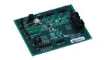
TPS65720EVM
The TPS65720EVM-515 evaluation module is a fully assembled and tested circuit for evaluating the
TPS65720 two-channel power management integrated circuit..
1
2
3
4
5
6
7
Contents
Introduction .................................................................................................................. 2
1.1
Requirements ....................................................................................................... 2
1.2
1.2 Applications .................................................................................................... 2
1.3
Features ............................................................................................................. 2
TPS65720EVM Electrical Performance Specifications ................................................................ 3
TPS65720EVM Schematic ................................................................................................ 4
Connector and Test Point Descriptions .................................................................................. 5
4.1
Enable Jumpers/Switches ........................................................................................ 5
Setup ......................................................................................................................... 7
5.1
Software Setup ..................................................................................................... 7
5.2
Hardware Setup .................................................................................................... 7
5.3
Running the Software ............................................................................................. 7
TPS65720EVM Assembly Drawings and Layout ...................................................................... 13
Bill of Materials ............................................................................................................. 16
List of Figures
................................................................................................
1
TPS65720EVM Schematic
2
Hardware Board Connection .............................................................................................. 7
4
3
Starting the Software ....................................................................................................... 8
4
Software Charger View ..................................................................................................... 9
5
Software DCDC1/LDO1 View ............................................................................................ 10
6
GPIO View.................................................................................................................. 11
7
INTERRUPTS VIEW ...................................................................................................... 12
8
TPS65720EVM Component Placement (Viewed From Top) ........................................................ 13
9
TPS65720EVM Top Copper (Viewed From Top) ..................................................................... 13
10
TPS65720EVM Bottom Copper (X-Ray View ) ........................................................................ 14
11
TPS65720EVM Internal 1 (X-Ray View From Top) ................................................................... 14
12
TPS65720VM Internal 2 (X-Ray View From Top) ..................................................................... 15
1
TPS65720EVM Electrical and Performance Specifications ........................................................... 3
2
HPA515B Bill of Materials ................................................................................................ 16
List of Tables
SLVU324 – March 2010
Submit Documentation Feedback
TPS65720EVM
Copyright © 2010, Texas Instruments Incorporated
1
�Introduction
1
Introduction
1.1
Requirements
www.ti.com
In order to operate this evaluation module (EVM), the following components must be connected and
properly configured. All components and connectors are supplied in the EVM except for the host computer
and the DC power supply. Software must be downloaded from the TI Web site at www.ti.com.
1.1.1
Software
To download the software that is necessary to operate the TPS65720EVM, check the TPS65720 product
folder on the TI Web site.
1.1.2
Host Computer
A personal computer (PC) with a USB port is required to operate this EVM. The TPS65720 software runs
on the PC and communicates with the EVM via the PC's USB port and the USB-to-GPIO interface.
PC Requirements :
• Windows™ 2000 or XP operating system
• USB port
• Minimum of 30 MB of free hard-disk space (100 MB recommended)
• Minimum of 256 MB of RAM
1.1.3
Power Supply Requirements
A DC power supply capable of delivering 5 V at 1 A is required to operate this EVM.
1.2
1.2 Applications
•
•
1.3
Features
•
•
•
•
•
•
•
2
Bluetooth Headsets
Handheld Applications
Input voltage rating
Output voltage adjustable via I2C Interface
Battery charger with power path Management
300-mA charge current
200-mA step-down converter for TPS65720
2.25-MHz Switching Frequency
1 General-purpose 200-mA LDO
TPS65720EVM
SLVU324 – March 2010
Submit Documentation Feedback
Copyright © 2010, Texas Instruments Incorporated
�TPS65720EVM Electrical Performance Specifications
www.ti.com
2
TPS65720EVM Electrical Performance Specifications
Table 1. TPS65720EVM Electrical and Performance Specifications
Parameter
Symbol
Notes and Conditions
Min
Typ
Max
Unit
Input Characteristics
Input Voltage AC
VAC
4.35
28
V
Input Voltage DCDC1
VIN_DCDC1
2.1
5.6
V
Input Voltage LDO1
VIN_LDO1
1.8
6.6
V
Input Current
IAC,max
Bit = 00
Bit = 01 or 10
UVLO
UVLO Hysteresis
90
95
100
450
475
500
3.3
3.45
V
mA
VUVLO
VAC rising
3.2
VHYS-UVLO
VAC falling
200
300
mV
2.2
5.6
V
3
%
2
%
200
mA
775
mA
180
mA
Output Characteristics
Voltage Range at SYS
VSYS
Output Voltage DCDC1
VDCDC1
VIN = Nom, IOUT = Nom
1.2
VIN = 2.3 V to 5.6 V, PFM operation,
0 mA to IOUT, max
Output Voltage Accuracy DCDC1
VIN = 2.3 V to 5.6 V, PWM operation,
0 mA to IOUT, max
Load Regulation
Output Current DCDC1
Forward Current Limit High-side
and Low-side MOSFET
-2
PWM operation
IOUT,DCDC1
ILIMF
Dropout Voltage LDO1
Default Output Voltage LDO1
1
0.5
VIN = Min to Max
VIN = 2.3 V to 5.6 V
425
600
VIN,LDO = 2.05 V, IOUT = 200 mA
VLDO1
VIN = Nom, IOUT = Nom
Output Voltage Accuracy LDO1
-1.5
Load Regulation LDO1
VIN = Nom, VOUT = VOUT2-5%
%
1.85
V
2.5
%
200
mA
-1
1
%
-1
2
%
Output Current of LDO1
Line Regulation LDO1
V
Systems Characteristics
Switching Frequency
FSW
Peak Efficiency
hpk
Full Load Efficiency
h
2030
2250
VIN =Nom
VIN = 3.6, VOUT = 2.05, IOUT = 400 mA
MIPSA25202R2
SLVU324 – March 2010
Submit Documentation Feedback
2480
92
89
TPS65720EVM
Copyright © 2010, Texas Instruments Incorporated
kHz
%
%
3
�TPS65720EVM Schematic
3
www.ti.com
TPS65720EVM Schematic
For Reference Only, See Table 2 for specific values.
Figure 1. TPS65720EVM Schematic
4
TPS65720EVM
SLVU324 – March 2010
Submit Documentation Feedback
Copyright © 2010, Texas Instruments Incorporated
�Connector and Test Point Descriptions
www.ti.com
4
Connector and Test Point Descriptions
4.1
Enable Jumpers/Switches
4.1.1
J1 – VIN
This header is the positive connection to the input power supply. The power supply must be connected
between J1 and J2 (GND). The leads to the input supply must be twisted and kept as short as possible.
The input voltage has to be between 4.35 V and 6 V.
4.1.2
J2 – GND
This header is the return connection to the input power supply. Connect the power supply between J2 and
J1 (VIN). The leads to the input supply must be twisted and kept as short as possible. The input voltage
has to be between 4.35 V and 6 V.
4.1.3
J3 – BAT / GND / TS
Connect your battery positive connection to pin 1 of J3, negative connection to pin 2 of J3. The battery
thermistor can be connected to pin 3 of J3. if an external thermistor is used, R2 must be removed.
4.1.4
J4 – SYS
This header is the positive output of the power path.
4.1.5
J5 – GND
This header is the negative output of the power path.
4.1.6
J6 – VIN_LDO1 / GND
This header is the input supply for the LDO1 on the EVM. VINLDO1 is directly connected to SYS with R4.
It also can be connected to VDCDC1 with R5. An external power supply can be connected between J6
pin1 (VINLDO) and pin2 (GND). Note that the resistors R4 and R5 must be removed when supplying the
LDO1 from an external power supply.
4.1.7
J7 – VDCDC1
This header is the positive output of VDCDC1 step-down converter. The output voltage of DCDC1 can be
adjusted to any voltage between 0.6 V and VINDCDC1 with the external voltage divider R7 and R8.
The default setting is 1.2 V. VDCDC1 is capable of sourcing up to 200 mA. A load can be connected
between J7 and J8 (GND).
4.1.8
J8 – GND
J8 is the return connection of VDCDC1 output rail. A load can be connected between J8 and J7
(VDCDC1).
4.1.9
J9 – VLDO
This header is the positive output of LDO1 linear regulator. The default output voltage of LDO1 is 1.85 V.
VLDO1 can be adjusted via I2C interface in the range between .
LDO1 is capable of sourcing up to 300 mA. A load can be connected between J9 and J10 (GND).
4.1.10
J10 – GND
J10 is the return connection of LDO1 output rail. A load can be connected between J10 and J9
(VDCDC1).
SLVU324 – March 2010
Submit Documentation Feedback
TPS65720EVM
Copyright © 2010, Texas Instruments Incorporated
5
�Connector and Test Point Descriptions
4.1.11
www.ti.com
J11 /INT / RESET / GND
J11 pin 1 is connected to the open-drain output /INT. J11 pin 2 is connected to the open-drain output
RESET. All open-drain outputs are pulled up with a resistor to the pullup voltage PULLUP. Pullup is
connected to VLDO1 with R10 on the EVM. Pullup also can be connected to VIN and VDCDC1 with the
resistors R20 and R21. J13 pin 3 is connected to GND.
4.1.12
J12 SYS/GPIO0/GPIO1/GPIO2/GPIO3/SYS
Four GPIOs are available on this header.
• J12 pin 1 is connected to the SYS voltage.
• J12 pin 2 is connected to GPIO0.
• J12 pin 3 is connected to GPIO1.
• J12 pin 4 is connected to GPIO2.
• J12 pin 5 is connected to GPIO3.
4.1.13
J13
J13 is the interface connector for the I2C interface. Connect a 10-pin ribbon cable between J13 and the
USB-to-GPIO interface.
4.1.14
JP1
JP1 connects the cathode of the LED D2 to GPIO2. If GPIO2 is configured as a current sink JP1 can be
removed to measure the current through the LED with an ammeter.
If GPIO2 is configured as an input or output, JP1 must be removed to disconnect the LED D2.
4.1.15
JP2
JP2 connects the cathode of the LED D1 to GPIO3. If GPIO3 is configured as a current sink, JP2 can be
removed to measure the current through the LED with an ammeter.
4.1.16
JP3 HOLD_DCDC1
Connect a shorting jumper between HOLD_DCDC1 and SYS to enable DCDC1. Note that if a power
supply is connected to AC, DCDC1 is enabled independent of the status of HOLD_DCDC1.
If the IC is supplied from BAT, DCDC1 is enabled when PB_IN is pulled low. To keep DCDC1 enabled,
HOLD_DCDC1 must be pulled high before /PB_IN is released high.
4.1.17
JP4 HOLD_LDO1
Connect a shorting jumper between HOLD_LDO1 and SYS to enable LDO1. Note that if a power supply is
connected to AC, LDO is enabled independent of the status of HOLD_LDO1.
If the IC is supplied from BAT, LDO is enabled when /PB_IN is pulled low. To keep LDO1 enabled,
HOLD_LDO11 must be pulled high before PB_IN is released high.
4.1.18
S1 – PB_IN
This is the pushbutton Input. Pressing S1 pulls PB_IN to GND and therefore enables DCDC1 and LDO1.
To keep DCDC1 / LDO1 enabled, the individual HOLD pins must be pulled high before PB_IN is released
high.
If a power supply is present at AC, both DCDC1 and LDO1 are enabled independent of the HOLD pins.
6
TPS65720EVM
SLVU324 – March 2010
Submit Documentation Feedback
Copyright © 2010, Texas Instruments Incorporated
�Setup
www.ti.com
5
Setup
5.1
Software Setup
To download the software, go the TPS65720 product folder on the TI Web site (www.ti.com).
Download the software, and execute it to install the software.
5.2
Hardware Setup
Host Computer
USB to GPIO Interface
TS
TPS65720EVM-515
+
J3
J13
Lithium Ion
Battery
J1
+
J2
-
DC Power Supply
Figure 2. Hardware Board Connection
5.3
Running the Software
Click on the TPS65720_1EVM icon to start the software. If no icon appears on the host computer, then
use the start button in the lower left corner of the screen to browse the program folders to find the
software. The default directory for software installation is Program Files\Texas
Instruments\TPS65720_1EVM.
Once the software is started, a dialog box appears (see Figure 3) and asks the user to select whether a
TPS65720 or TPS65721 is connected.
SLVU324 – March 2010
Submit Documentation Feedback
TPS65720EVM
Copyright © 2010, Texas Instruments Incorporated
7
�Setup
www.ti.com
Figure 3. Starting the Software
Once the used device is selected, the software starts up (see Figure 4).
By clicking on the Tabs CHARGER , DCDC1/LDO1, GPIO, and INTERRUPTS, the user can navigate
through the different Views
The window that first appears allows control of all charger settings and shows all the charger status Flags.
In the CHARGER Tab, users can enable/disable the charger and change charger parameters as regulated
output voltage on the Power Path (VSYS), Charge Voltage, Safety Timers, etc.
In the Lower right corner of the window, all charger related User Registers are displayed.
See the TPS65720 data sheet for detailed description on these registers.
8
TPS65720EVM
SLVU324 – March 2010
Submit Documentation Feedback
Copyright © 2010, Texas Instruments Incorporated
�Setup
www.ti.com
Figure 4. Software Charger View
The DCDC1/LDO1 control window (see Figure 5) allows control of operating mode (PWM/PFM) for the
DC/DC converter, output voltage of LDO1 (TPS65720 only) and shows the Status Flags related to DCDC1
and LDO1.
In the lower right corner of the window, all DCDC1/LDO1-related User Registers are displayed.
See the TPS65720 data sheet for detailed description on these registers.
SLVU324 – March 2010
Submit Documentation Feedback
TPS65720EVM
Copyright © 2010, Texas Instruments Incorporated
9
�Setup
www.ti.com
Figure 5. Software DCDC1/LDO1 View
The GPIO control window (see Figure 6) allows control of the fours GPIOs of the TPS65720/1. The GPIOs
can be configured as input or output. In addition, GPIO2 and GPIO3 can be configured as current sink to
drive an external LED.
In the lower right corner of the window, all GPIO-related User Registers are displayed.
See the TPS65720 data sheet for detailed description on these registers.
10
TPS65720EVM
SLVU324 – March 2010
Submit Documentation Feedback
Copyright © 2010, Texas Instruments Incorporated
�Setup
www.ti.com
Figure 6. GPIO View
The INTERRUPT control window allows the user to configure and mask interrupts.
In the default setup, all interrupts are masked.
If an event is masked, it is ignored and no interrupt is generated. If an event is not masked, an interrupt is
generated based on that event.
If any interrupt is pending, the INT pin is driven low. In the lower right corner of the window, all
INTERRUPT-related User Registers are displayed.
See the TPS65720 data sheet for detailed description on these registers.
SLVU324 – March 2010
Submit Documentation Feedback
TPS65720EVM
Copyright © 2010, Texas Instruments Incorporated
11
�Setup
www.ti.com
Figure 7. INTERRUPTS VIEW
12
TPS65720EVM
SLVU324 – March 2010
Submit Documentation Feedback
Copyright © 2010, Texas Instruments Incorporated
�TPS65720EVM Assembly Drawings and Layout
www.ti.com
6
TPS65720EVM Assembly Drawings and Layout
The following figures (Figure 8 through Figure 12) show the design of the TPS65720EVM printed-circuit
board.
TEXAS
INSTRUMENTS
Figure 8. TPS65720EVM Component Placement (Viewed From Top)
Figure 9. TPS65720EVM Top Copper (Viewed From Top)
SLVU324 – March 2010
Submit Documentation Feedback
TPS65720EVM
Copyright © 2010, Texas Instruments Incorporated
13
�TPS65720EVM Assembly Drawings and Layout
www.ti.com
Figure 10. TPS65720EVM Bottom Copper (X-Ray View )
Figure 11. TPS65720EVM Internal 1 (X-Ray View From Top)
14
TPS65720EVM
SLVU324 – March 2010
Submit Documentation Feedback
Copyright © 2010, Texas Instruments Incorporated
�TPS65720EVM Assembly Drawings and Layout
www.ti.com
Figure 12. TPS65720VM Internal 2 (X-Ray View From Top)
SLVU324 – March 2010
Submit Documentation Feedback
TPS65720EVM
Copyright © 2010, Texas Instruments Incorporated
15
�Bill of Materials
7
www.ti.com
Bill of Materials
Table 2. HPA515B Bill of Materials
Count
RefDes
Value
Description
Size
Part Number
MFR
0
C1
open
Capacitor, Ceramic, 35V, X5R, 10%
0603
GMK107BJ105K
Taiyo Yuden
1
C10
2.2µF
Capacitor, Ceramic, 6.3V, X5R, 10%
0805
GRM155R60J22ME15D
Murata
1
C11
22µF
Capacitor, Ceramic, 50V, COG, 5%
0603
GRM1885C1H220JA01D
Murata
1
C2
1µF
Capacitor, Ceramic, 35V, X5R, 10%
0603
GMK107BJ105K
Taiyo Yuden
1
C3
1µF
Capacitor, Ceramic, 6.3V, X5R, 10%
0603
JMK107BJ105KK-T
Taiyo Yuden
1
C4
open
Capacitor, Ceramic, 6.3V, X5R, 10%
0603
GRM188R60J475K
Murata
2
C5, C8
4.7µF
Capacitor, Ceramic, 6.3V, X5R, 10%
0603
GRM188R60J475K
Murata
1
C6
10µF
Capacitor, Ceramic, 6.3V, X5R, 20%
0603
GRM188R60J106ME47D
Murata
0
C7
open
Capacitor, Ceramic, 6.3V, X5R, 20%
0805
GRM188R60J106ME47D
Murata
0
C9
open
Capacitor, Ceramic, 6.3V, X7R, 10%
0805
GRM188R60J225KE19D
Murata
1
D1
LTL29S
Diode LED, red, 60 mW, 15mA
0603
LT L29S-N2Q1-25
Osram
1
D2
LSL29
Diode LED, green. 40 mW, 20mA
0603
LS L29K-G1H2-1
Osram
9
J1- J10
PTC36SAAN
Header, Male 2-pin, 100mil spacing
0.100 inch x 2
PEC02SAAN
Sullins
1
J12
PTC36SAAN
Header, Male 6-pin, 100mil spacing
0.100 inch x 6
PEC06SAAN
Sullins
1
J13
PTC36DAAN
Connector, Male straight 2c5 pin, 100mil
spacing, 4 wall
0.100 inch x 5
X2
2510-6002RB
3M
2
J3, J11
PTC36SAAN
Header, 3-pin, 100mil spacing
0.100 inch x 3
PEC03SAAN
Sullins
2
JP1, JP2
PEC03SAAN
Header, 2-pin, 100mil spacing
0.100 inch x 2
PEC02SAAN
Sullins
2
JP3, JP4
PEC03SAAN
Header, 3-pin, 100mil spacing
0.100 inch x 3
PEC03SAAN
Sullins
1
L1
2.2µH
Inductor, Power, xx A, yy milliohms
2.5 × 2.0 mm
MIPSA2520D1R0
FDK
0
R1, R5, R13,
R14, R20, R21
open
Resistor, Chip, 1/16W, 1%
0603
std
std
1
R10
open
Resistor, Chip, 1/16W, 5%
0603
std
std
2
R17, R18
3.3k
Resistor, Chip, 1/16W, 5%
0603
std
std
1
R2
10k
Resistor, Chip, 1/16W, 1%
0603
std
std
1
R3
1k
Resistor, Chip, 1/16W, 1%
0603
std
std
2
R4, R19
0
Resistor, Chip, 1/16W, 1%
0603
std
std
5
R6, R11, R12,
R15, R16
100k
Resistor, Chip, 1/16W, 1%
0603
std
std
2
R7, R8
330k
Resistor, Chip, 1/16W, 1%
0603
std
std
1
R9
0
Resistor, Chip, 1/16W, 5%
0603
std
std
1
S1
KT11P2JM
Switch, SPST, PB Momentary, Sealed Tactile
0.245 X 0.251
inch
KT11P2JM34LFS
C&K
1
U1
TPS65720YFF
IC, PMU for Bluetooth Headsets
DSBGA-25
TPS65720YFF
TI
1
--
PCB, 2 In x 2 In x 0.062 In
HPA515
Any
3
--
Shunt, 100-mil, Black
929950-00
3M
0.100
Notes 1. These assemblies are ESD sensitive, ESD precautions shall be observed.
2. These assemblies must be clean and free from flux and all contaminants.
Using unclean flux is unacceptable.
3. These assemblies must comply with workmanship standards IPC-A-610 Class 2.
4. Ref designators marked with an asterisk ('**') cannot be substituted.
All other components can be substituted with equivalent MFG's components.
5 Maximum 30 grams placement pressure on DSBGA-25 parts.
16
TPS65720EVM
SLVU324 – March 2010
Submit Documentation Feedback
Copyright © 2010, Texas Instruments Incorporated
�Evaluation Board/Kit Important Notice
Texas Instruments (TI) provides the enclosed product(s) under the following conditions:
This evaluation board/kit is intended for use for ENGINEERING DEVELOPMENT, DEMONSTRATION, OR EVALUATION
PURPOSES ONLY and is not considered by TI to be a finished end-product fit for general consumer use. Persons handling the
product(s) must have electronics training and observe good engineering practice standards. As such, the goods being provided are
not intended to be complete in terms of required design-, marketing-, and/or manufacturing-related protective considerations,
including product safety and environmental measures typically found in end products that incorporate such semiconductor
components or circuit boards. This evaluation board/kit does not fall within the scope of the European Union directives regarding
electromagnetic compatibility, restricted substances (RoHS), recycling (WEEE), FCC, CE or UL, and therefore may not meet the
technical requirements of these directives or other related directives.
Should this evaluation board/kit not meet the specifications indicated in the User’s Guide, the board/kit may be returned within 30
days from the date of delivery for a full refund. THE FOREGOING WARRANTY IS THE EXCLUSIVE WARRANTY MADE BY
SELLER TO BUYER AND IS IN LIEU OF ALL OTHER WARRANTIES, EXPRESSED, IMPLIED, OR STATUTORY, INCLUDING
ANY WARRANTY OF MERCHANTABILITY OR FITNESS FOR ANY PARTICULAR PURPOSE.
The user assumes all responsibility and liability for proper and safe handling of the goods. Further, the user indemnifies TI from all
claims arising from the handling or use of the goods. Due to the open construction of the product, it is the user’s responsibility to
take any and all appropriate precautions with regard to electrostatic discharge.
EXCEPT TO THE EXTENT OF THE INDEMNITY SET FORTH ABOVE, NEITHER PARTY SHALL BE LIABLE TO THE OTHER
FOR ANY INDIRECT, SPECIAL, INCIDENTAL, OR CONSEQUENTIAL DAMAGES.
TI currently deals with a variety of customers for products, and therefore our arrangement with the user is not exclusive.
TI assumes no liability for applications assistance, customer product design, software performance, or infringement of
patents or services described herein.
Please read the User’s Guide and, specifically, the Warnings and Restrictions notice in the User’s Guide prior to handling the
product. This notice contains important safety information about temperatures and voltages. For additional information on TI’s
environmental and/or safety programs, please contact the TI application engineer or visit www.ti.com/esh.
No license is granted under any patent right or other intellectual property right of TI covering or relating to any machine, process, or
combination in which such TI products or services might be or are used.
FCC Warning
This evaluation board/kit is intended for use for ENGINEERING DEVELOPMENT, DEMONSTRATION, OR EVALUATION
PURPOSES ONLY and is not considered by TI to be a finished end-product fit for general consumer use. It generates, uses, and
can radiate radio frequency energy and has not been tested for compliance with the limits of computing devices pursuant to part 15
of FCC rules, which are designed to provide reasonable protection against radio frequency interference. Operation of this
equipment in other environments may cause interference with radio communications, in which case the user at his own expense
will be required to take whatever measures may be required to correct this interference.
EVM Warnings and Restrictions
It is important to operate this EVM within the input voltage range of 4.35 V to 28 V and the output voltage range of 0.6 V to 5.6 V .
Exceeding the specified input range may cause unexpected operation and/or irreversible damage to the EVM. If there are
questions concerning the input range, please contact a TI field representative prior to connecting the input power.
Applying loads outside of the specified output range may result in unintended operation and/or possible permanent damage to the
EVM. Please consult the EVM User's Guide prior to connecting any load to the EVM output. If there is uncertainty as to the load
specification, please contact a TI field representative.
During normal operation, some circuit components may have case temperatures greater than 60° C. The EVM is designed to
operate properly with certain components above 60° C as long as the input and output ranges are maintained. These components
include but are not limited to linear regulators, switching transistors, pass transistors, and current sense resistors. These types of
devices can be identified using the EVM schematic located in the EVM User's Guide. When placing measurement probes near
these devices during operation, please be aware that these devices may be very warm to the touch.
Mailing Address: Texas Instruments, Post Office Box 655303, Dallas, Texas 75265
Copyright © 2010, Texas Instruments Incorporated
�IMPORTANT NOTICE
Texas Instruments Incorporated and its subsidiaries (TI) reserve the right to make corrections, modifications, enhancements, improvements,
and other changes to its products and services at any time and to discontinue any product or service without notice. Customers should
obtain the latest relevant information before placing orders and should verify that such information is current and complete. All products are
sold subject to TI’s terms and conditions of sale supplied at the time of order acknowledgment.
TI warrants performance of its hardware products to the specifications applicable at the time of sale in accordance with TI’s standard
warranty. Testing and other quality control techniques are used to the extent TI deems necessary to support this warranty. Except where
mandated by government requirements, testing of all parameters of each product is not necessarily performed.
TI assumes no liability for applications assistance or customer product design. Customers are responsible for their products and
applications using TI components. To minimize the risks associated with customer products and applications, customers should provide
adequate design and operating safeguards.
TI does not warrant or represent that any license, either express or implied, is granted under any TI patent right, copyright, mask work right,
or other TI intellectual property right relating to any combination, machine, or process in which TI products or services are used. Information
published by TI regarding third-party products or services does not constitute a license from TI to use such products or services or a
warranty or endorsement thereof. Use of such information may require a license from a third party under the patents or other intellectual
property of the third party, or a license from TI under the patents or other intellectual property of TI.
Reproduction of TI information in TI data books or data sheets is permissible only if reproduction is without alteration and is accompanied
by all associated warranties, conditions, limitations, and notices. Reproduction of this information with alteration is an unfair and deceptive
business practice. TI is not responsible or liable for such altered documentation. Information of third parties may be subject to additional
restrictions.
Resale of TI products or services with statements different from or beyond the parameters stated by TI for that product or service voids all
express and any implied warranties for the associated TI product or service and is an unfair and deceptive business practice. TI is not
responsible or liable for any such statements.
TI products are not authorized for use in safety-critical applications (such as life support) where a failure of the TI product would reasonably
be expected to cause severe personal injury or death, unless officers of the parties have executed an agreement specifically governing
such use. Buyers represent that they have all necessary expertise in the safety and regulatory ramifications of their applications, and
acknowledge and agree that they are solely responsible for all legal, regulatory and safety-related requirements concerning their products
and any use of TI products in such safety-critical applications, notwithstanding any applications-related information or support that may be
provided by TI. Further, Buyers must fully indemnify TI and its representatives against any damages arising out of the use of TI products in
such safety-critical applications.
TI products are neither designed nor intended for use in military/aerospace applications or environments unless the TI products are
specifically designated by TI as military-grade or "enhanced plastic." Only products designated by TI as military-grade meet military
specifications. Buyers acknowledge and agree that any such use of TI products which TI has not designated as military-grade is solely at
the Buyer's risk, and that they are solely responsible for compliance with all legal and regulatory requirements in connection with such use.
TI products are neither designed nor intended for use in automotive applications or environments unless the specific TI products are
designated by TI as compliant with ISO/TS 16949 requirements. Buyers acknowledge and agree that, if they use any non-designated
products in automotive applications, TI will not be responsible for any failure to meet such requirements.
Following are URLs where you can obtain information on other Texas Instruments products and application solutions:
Products
Applications
Amplifiers
amplifier.ti.com
Audio
www.ti.com/audio
Data Converters
dataconverter.ti.com
Automotive
www.ti.com/automotive
DLP® Products
www.dlp.com
Communications and
Telecom
www.ti.com/communications
DSP
dsp.ti.com
Computers and
Peripherals
www.ti.com/computers
Clocks and Timers
www.ti.com/clocks
Consumer Electronics
www.ti.com/consumer-apps
Interface
interface.ti.com
Energy
www.ti.com/energy
Logic
logic.ti.com
Industrial
www.ti.com/industrial
Power Mgmt
power.ti.com
Medical
www.ti.com/medical
Microcontrollers
microcontroller.ti.com
Security
www.ti.com/security
RFID
www.ti-rfid.com
Space, Avionics &
Defense
www.ti.com/space-avionics-defense
RF/IF and ZigBee® Solutions www.ti.com/lprf
Video and Imaging
www.ti.com/video
Wireless
www.ti.com/wireless-apps
Mailing Address: Texas Instruments, Post Office Box 655303, Dallas, Texas 75265
Copyright © 2010, Texas Instruments Incorporated
�