User's Guide
SLVU486A – July 2011 – Revised July 2011
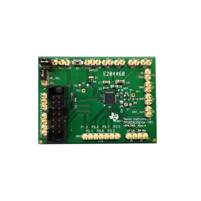
TPS65835 System Evaluation Board
This user’s guide describes the characteristics, operation, and use of the TPS65835EVM-705 evaluation
module (EVM). The TPS65835EVM-705 is a fully assembled and tested platform for evaluating the
performance of the TPS65835 single-chip power management device. This document includes schematic
diagrams, a printed circuit board (PCB) layout, bill of materials, and test data. Throughout this document,
the abbreviations EVM, TPS65835EVM, and the term evaluation module are synonymous with the
TPS65835EVM-705 unless otherwise noted.
1
2
3
4
5
6
7
8
Contents
Introduction .................................................................................................................. 3
1.1
Features ............................................................................................................. 3
1.2
Applications ......................................................................................................... 3
1.3
Requirements ....................................................................................................... 3
Electrical Performance Specifications .................................................................................... 3
Schematic .................................................................................................................... 4
Connector and Test Point Descriptions .................................................................................. 5
4.1
Headers and Switch ............................................................................................... 5
4.2
Jumpers ............................................................................................................. 6
4.3
Test Points .......................................................................................................... 6
Setup ......................................................................................................................... 6
TPS65835EVM Test Data ................................................................................................. 7
6.1
Operation Waveforms ............................................................................................. 7
6.2
Measured Data ................................................................................................... 13
6.3
Thermal Performance ............................................................................................ 14
EVM Assembly Drawings and Layout .................................................................................. 15
Bill of Materials ............................................................................................................. 17
List of Figures
1
Schematic .................................................................................................................... 4
2
Boost Output Ripple : Vbat = 3.2 V and 1 mA Load on Boost ........................................................ 7
3
Startup : Vin = 5 V, 1 mA Load on Boost, and 15 mA Load on LDO ................................................ 8
4
Shutdown : Vin = 5 V, 1 mA Load on Boost, and 15 mA Load on LDO ............................................. 8
5
Startup : Vbat = 3.6 V, 1 mA Load on Boost, and 15 mA Load on LDO
6
Shutdown : Vbat = 3.6 V, 1 mA Load on Boost, and 15 mA Load on LDO ......................................... 9
7
Switch node : Vbat = 3.6 V, No Load, 0.5µs/div....................................................................... 10
8
Switch node : Vbat = 3.6 V, No Load, 10 µs/div
9
Load Transient, Boost : Vbat = 3.6 V with 0 mA to 5 mA Transient, Constant 15 mA Load on LDO. CH3
Bstout CH4 IBOOST .......................................................................................................... 11
10
Load Transient, Boost : Vbat = 3.6 V with 5 mA to 0mA Transient, Constant 15 mA Load on LDO. CH3
Bstout CH4 IBOOST .......................................................................................................... 11
11
Load Transient, LDO : Vbat = 3.6 V with 0 mA to 30 mA Transient. CH3 VLDO, CH4 IVLDO ................. 12
12
Load Transient, LDO : Vbat = 3.6 V with 30 mA to 0 mA Transient. CH3 VLDO, CH4 IVLDO .................... 12
13
H-Bridge Operation : Ch. 1 - LCLP, Ch 2 - LCLN, Ch 3 - LCRP, Ch 4 - LCRN................................... 13
14
Load Regulation ........................................................................................................... 13
15
Thermal Performance – Top Side ....................................................................................... 14
SLVU486A – July 2011 – Revised July 2011
Submit Documentation Feedback
............................................
......................................................................
TPS65835 System Evaluation Board
Copyright © 2011, Texas Instruments Incorporated
9
10
1
�www.ti.com
16
Thermal Performance – Bottom Side ................................................................................... 15
17
Top Assembly – Silkscreen .............................................................................................. 15
18
Top Layer ................................................................................................................... 16
19
Bottom Layer ............................................................................................................... 16
List of Tables
2
1
Bill of Materials............................................................................................................. 17
2
Evaluation Materials ....................................................................................................... 17
TPS65835 System Evaluation Board
Copyright © 2011, Texas Instruments Incorporated
SLVU486A – July 2011 – Revised July 2011
Submit Documentation Feedback
�Introduction
www.ti.com
1
Introduction
The TPS65835 is a single-chip power management IC for active lens 3D glasses consisting of a battery
charger with Power Path management for a single lithium-ion (Li-Ion) or lithium-polymer (Li-Polymer) or
standard coin cell, a low drop out linear regulator (LDO), a boost converter, two H-bridges an MSP430
Core.
1.1
Features
•
•
•
•
•
1.2
Applications
•
1.3
Battery Charger
– Power Path management
Low Dropout Linear Regulator (LDO)
Boost Converter
Two H-Bridges
MSP430 Core
Active 3D glasses
– Television
– Computer
– Handheld
– Theater
– Gaming
Requirements
In order to operate this EVM properly, the hardware must be connected and properly configured. All
components and connectors are installed on the EVM as shipped, except the dc power supply.
2
Electrical Performance Specifications
Input Voltage VIN 3.7 to 6.4 V
Input Voltage Vbat BAT 2.5 to 6.4 V
Output Voltage LDO VLDO 2.2 (default) or 3 V
Output Voltage Boost BST_OUT 8 to 16 V, 10 V default
Charge Current ICHG = Kiset/Riset 5 to 100 mA, 70 mA default
Input Voltage Low VIL (SW_SEL, VLDO_SET) 0.4 V
Input Voltage High VIH (SW_SEL, VLDO_SET) 1.2 V
SLVU486A – July 2011 – Revised July 2011
Submit Documentation Feedback
TPS65835 System Evaluation Board
Copyright © 2011, Texas Instruments Incorporated
3
�Schematic
3
www.ti.com
Schematic
Figure 1. Schematic
4
TPS65835 System Evaluation Board
Copyright © 2011, Texas Instruments Incorporated
SLVU486A – July 2011 – Revised July 2011
Submit Documentation Feedback
�Connector and Test Point Descriptions
www.ti.com
4
Connector and Test Point Descriptions
4.1
Headers and Switch
J1 : VIN
J1 pin 1 and pin 2 are VIN of the TPS65835. Connect the VIN (Charger) power supply positive terminal to
J1.
J2 : GND
J2 pin 1 and pin 2 are GND of the TPS65835. Connect the VIN (Charger) power supply negative terminal
to J2.
J3 : BAT
J3 pin 1 and pin 2 are BAT of the TPS65835. Connect the second power supply (Battery)(capable of
sinking current) positive terminal to J3.
J4 : GND
J4 pin 1 and pin 2 are GND of the TPS65835. Connect the second power supply (Battery)(capable of
sinking current) negative terminal to J4.
J5 : GND
J5 pin 1 and pin 2 are GND of the TPS65835. These are provided as an extra set of ground terminals.
J6 : LP, LN
J6 pin 1 is LCLP, liquid crystal left positive, of the TPS65835 and pin 2 is LCLN, liquid crystal left negative,
of the TPS65835. Connect the left lens across pin 1 and 2 of header J6.
J7 : RP, RN
J7 pin 1 is LCRP, liquid crystal right positive, of the TPS65835 and pin 2 is LCRN, liquid crystal right
negative, of the TPS65835. Connect the left lens across pin 1 and 2 of the J7.
J8 : BST_OUT
J8 pin 1 and pin 2 are BST_OUT of the TPS65835. In a typical application, the boost will be loaded only
through the h-bridge on pins LCLP, LPLN, LCRP,LCRN (J6,J7) by the liquid crystal lenses.
J9 : GND
J9 pin 1 and pin 2 are GND.
J10 : VLDO, GND
J10 pin 1 is GND and pin 2 is VLDO, the output of the TPS65835 LDO.
J11 (3-pin header): SWITCH, HIGH, LOW
J11 pin 1 is GND, pin 2 is the SWITCH pin of the TPS65835 and pin 3 is the SYS voltage output of the
TPS65835. This header, J11, is to simulate the use of a slide switch and should only be used when JP1
pins 1 and 2 are shorted. If instead, a push-button switch is used, J11 should be left open and the
push-button will pull SWITCH to GND when pressed and release (float) it otherwise (SWITCH has an
internal pull-up only when JP1 pins 2 and 3 are shorted). Note there is an alternate configuration for J11.
S1: Push-Button Switch
S1 is the push-button switch connected to the SWITCH pin of the TPS65835. When the button on S1 is
pressed, the SWITCH pin is connected to ground for the duration that the button is held. When the button
is released, the SWITCH pin goes back up to SYS. S1 should only be used if JP1 is in the S1 position (pin
2 and pin 3 shorted of JP1).
J12 : TS, GND
J12 pin 1 is GND, pin 2 is the TS pin of the TPS65835. This header, J12, is to connect an external
thermistor to the TPS65835 and should be left floating if not used.
J13 : GPIOs P1.1, P1.2, P1.4
J13 pin 1 is P1.4, pin 2 is P1.2 and pin 3 is P1.1 of the TPS65835 MSP430 core.
The functionality of these GPIOs is discussed in the TPS65835 datasheet and the MSP430x2xx family
user's guide.
J14 : GPIOs P1.4, P1.5, P1.6, P1.7
SLVU486A – July 2011 – Revised July 2011
Submit Documentation Feedback
TPS65835 System Evaluation Board
Copyright © 2011, Texas Instruments Incorporated
5
�Setup
www.ti.com
J14 pin 1 is P1.7, pin 2 is P1.6, pin 3 is P1.5 and pin 4 is P1.4 of the TPS65835 MSP430 core. The
functionality of these GPIOs is discussed in the TPS65835 datasheet and the MSP430x2xx family user's
guide.
J15 : J-TAG Connector for USB Programming Tool (MSP-FET430UIF)
J15 is a keyed header for the MSP-FET430UIF USB Programming Tool.
J16 : GPIOs P1.3, P2.2, P2.3, P2.6, P2.7, P3.3, P3.5
J16 pin 1 is P3.5, pin 2 is P3.3, pin 3 is P2.7, pin 4 is P2.6, pin 5 is P2.3, pin 6 is P2.2 and pin 7 is P1.3 of
the TPS65835 MSP430 core. The functionality of these GPIOs is discussed in the TPS65835 datasheet
and the MSP430x2xx family user's guide.
4.2
Jumpers
JP1 : SW_SEL, S1, JP11
JP1 pin 1 is GND, pin 2 is the SW_SEL pin of the TPS65835 and pin 3 is the SYS voltage output of the
TPS65835. Short pins 1 and 2 to use a slide switch on SWICTH pin of TPS65835 or short pins 2 and 3 to
use the installed push-button switch S1 on SWITCH pin of TPS65835.
JP2 : VLDO_SET, 2.2V, 3.0V
JP2 pin 1 is GND, pin 2 is the VLDO_SET pin of the TPS65835 and pin 3 is the SYS voltage output of the
TPS65835. Short pins 1 and 2 to set the LDO output voltage to 2.2V or short pins 2 and 3 to set the LDO
output voltage to 3.0V.
4.3
Test Points
TP1 : When R5 is replaced with a 50-Ω resistor, TP1 is used to inject an AC signal which may be
measured at BST_OUT to verify frequency response and converter stability.
TP2 : When D2 is populated, TP2 can be used to connect a microcontroller GPIO to implement special
push-button power/on power off timing.
5
Setup
Set the first input power supply voltage to 5 V before connecting the EVM then power it off. Connect the
positive lead to J1, VIN. The power supply return lead is connected to J2 GND.
Set the second input power supply (capable of sinking capable of sinking at least 200 mA) to 3.6 V before
connecting to the EVM then power it off. The positive lead is connected to J3, BAT. The power supply
return lead is connected to J4, GND.
Apply 5V to the VIN input.
With JP2-VLDO_SET set to 3.0V, verify with voltmeter that the VLDO output voltage is 3V ± 100 mV.
Position JP2 shorting jumper between VLDO_SET and 2.2V. Verify with voltmeter that the VLDO output
voltage is 2.2V ± 100m V.
Verify that input current is less than 50mA with and input voltage of 5 V.
Verify JP1 is set with S1 and SWITCH shorted, press the push-button (S1) and verify with voltmeter that
the output voltage is 10V ± 1 V.
Verify LCLP is toggling between 10 V ± 1 V and 0V ± 1 V.
Verify LCLN is toggling between 10 V ± 1 V and 0V ± 1 V.
Verify LCRP is toggling between 10 V ± 1 V and 0V ± 1 V.
Verify LCRN is toggling between 10 V ± 1 V and 0V ± 1 V.
Set input voltage supply capable of sinking at least 500mA on BAT to 3.6 V and power on.
Verify that input current is less than 200mA with input voltage of 5 V VIN power supply. Verify D1 lights up
to indicate charging.
6
TPS65835 System Evaluation Board
Copyright © 2011, Texas Instruments Incorporated
SLVU486A – July 2011 – Revised July 2011
Submit Documentation Feedback
�TPS65835EVM Test Data
www.ti.com
6
TPS65835EVM Test Data
This section presents typical performance data for the TPS65835EVM. Actual performance data can be
affected by measurement techniques and environmental variables; therefore, these results are presented
for reference and may differ from actual results obtained by some users.
6.1
Operation Waveforms
Figure 2. Boost Output Ripple : Vbat = 3.2 V and 1 mA Load on Boost
SLVU486A – July 2011 – Revised July 2011
Submit Documentation Feedback
TPS65835 System Evaluation Board
Copyright © 2011, Texas Instruments Incorporated
7
�TPS65835EVM Test Data
www.ti.com
Figure 3. Startup : Vin = 5 V, 1 mA Load on Boost, and 15 mA Load on LDO
Figure 4. Shutdown : Vin = 5 V, 1 mA Load on Boost, and 15 mA Load on LDO
8
TPS65835 System Evaluation Board
Copyright © 2011, Texas Instruments Incorporated
SLVU486A – July 2011 – Revised July 2011
Submit Documentation Feedback
�TPS65835EVM Test Data
www.ti.com
Figure 5. Startup : Vbat = 3.6 V, 1 mA Load on Boost, and 15 mA Load on LDO
Figure 6. Shutdown : Vbat = 3.6 V, 1 mA Load on Boost, and 15 mA Load on LDO
SLVU486A – July 2011 – Revised July 2011
Submit Documentation Feedback
TPS65835 System Evaluation Board
Copyright © 2011, Texas Instruments Incorporated
9
�TPS65835EVM Test Data
www.ti.com
Figure 7. Switch node : Vbat = 3.6 V, No Load, 0.5µs/div
Figure 8. Switch node : Vbat = 3.6 V, No Load, 10 µs/div
10
TPS65835 System Evaluation Board
Copyright © 2011, Texas Instruments Incorporated
SLVU486A – July 2011 – Revised July 2011
Submit Documentation Feedback
�TPS65835EVM Test Data
www.ti.com
Figure 9. Load Transient, Boost : Vbat = 3.6 V with 0 mA to 5 mA Transient,
Constant 15 mA Load on LDO. CH3 Bstout CH4 IBOOST
Figure 10. Load Transient, Boost : Vbat = 3.6 V with 5 mA to 0mA Transient,
Constant 15 mA Load on LDO. CH3 Bstout CH4 IBOOST
SLVU486A – July 2011 – Revised July 2011
Submit Documentation Feedback
TPS65835 System Evaluation Board
Copyright © 2011, Texas Instruments Incorporated
11
�TPS65835EVM Test Data
www.ti.com
Figure 11. Load Transient, LDO : Vbat = 3.6 V with 0 mA to 30 mA Transient.
CH3 VLDO, CH4 IVLDO
Figure 12. Load Transient, LDO : Vbat = 3.6 V with 30 mA to 0 mA Transient.
CH3 VLDO, CH4 IVLDO
12
TPS65835 System Evaluation Board
Copyright © 2011, Texas Instruments Incorporated
SLVU486A – July 2011 – Revised July 2011
Submit Documentation Feedback
�TPS65835EVM Test Data
www.ti.com
Figure 13. H-Bridge Operation : Ch. 1 - LCLP, Ch 2 - LCLN, Ch 3 - LCRP, Ch 4 - LCRN
6.2
Measured Data
10.3
VO - Output Voltage - V
10.2
VBAT 2.5 V
10.1
VBAT 3.6 V
10
VBAT 6.4 V
9.9
9.8
9.7
0
0.001
0.002
0.003
0.004
0.005
0.006
IL - Load Current - A
Figure 14. Load Regulation
SLVU486A – July 2011 – Revised July 2011
Submit Documentation Feedback
TPS65835 System Evaluation Board
Copyright © 2011, Texas Instruments Incorporated
13
�TPS65835EVM Test Data
6.3
www.ti.com
Thermal Performance
Figure 15 and Figure 16 show the typical thermal performance for the TPS65835 for both the top side and
the bottom side, respectively. VIN = 5 V, KISET = 6.49 kΩ, VBAT = 3.6 V, ILDO = 30 mA and IBST_OUT = 5
mA.
6.3.1
Top Side
Figure 15. Thermal Performance – Top Side
14
TPS65835 System Evaluation Board
Copyright © 2011, Texas Instruments Incorporated
SLVU486A – July 2011 – Revised July 2011
Submit Documentation Feedback
�EVM Assembly Drawings and Layout
www.ti.com
6.3.2
Bottom Side
Figure 16. Thermal Performance – Bottom Side
7
EVM Assembly Drawings and Layout
Figure 17. Top Assembly – Silkscreen
SLVU486A – July 2011 – Revised July 2011
Submit Documentation Feedback
TPS65835 System Evaluation Board
Copyright © 2011, Texas Instruments Incorporated
15
�EVM Assembly Drawings and Layout
www.ti.com
Figure 18. Top Layer
Figure 19. Bottom Layer
16
TPS65835 System Evaluation Board
Copyright © 2011, Texas Instruments Incorporated
SLVU486A – July 2011 – Revised July 2011
Submit Documentation Feedback
�Bill of Materials
www.ti.com
8
Bill of Materials
Table 1. Bill of Materials
Count
RefDes
Value
Description
Size
Part Number
MFR
1
C1
2.2 µF
Capacitor, Ceramic, 25V, X5R, 10%
0805
GRM219R61E225KA12D
Murata
1
C2
2.2 µF
Capacitor, Ceramic, 10V, X7R, 10%
0603
GRM188R71A225KE15D
Murata
1
C3
4.7 µF
Capacitor, Ceramic, 10V, X7R, 20%
0805
C2012X7R1A475M
TDK
1
C4
4.7 µF
Capacitor, Ceramic, 25V, X5R, 10%
0805
Std
Std
1
C5
2.2 nF
Capacitor, Ceramic, Low Inductance,
50V, X5R, 10%
0603
GRM188R61H222KA01B
Murata
1
C6
10 µF
Capacitor, Ceramic, 16V, X5R, 20%
1206
Std
Std
1
L1
10 µH
Inductor, 1.066Ohm , 350mA, 20%
0805
CBC2016T100M
Taiyo Yuden
1
R1
1.82M
Resistor, Chip, 1/16W, 1%
0603
Std.
Std
1
R2
243k
Resistor, Chip, 1/16W, 1%
0603
Std.
Std
1
R3
6.49K
Resistor, Chip, 1/16W, 1%
0603
Std
Std
1
R5
47K
Resistor, Chip, 1/16W, 5%
0402
Std
Std
1
S1
688-SKRELG
Switch, SPST, PB Momentary
0.140 X 0.173 inch
688-SKRELG
Alps
1
U1
TPS65835RKP
IC, Advance PMU for Active Shutter 3D
Glasses
QFN-40
TPS65835RKP
TI
Table 2. Evaluation Materials
Count
RefDes
Value
Description
Size
Part Number
MFR
1
D1
LTST-C190CKT
Diode, LED, Red, 2.1-V, 20-mA, 6-mcd
0603
LTST-C190CKT
Lite On
0
D2
Open
Diode, Zener
SOD-123
STD
STD
11
J1-J10, J12
PEC02SAAN
Header, Male 2-pin, 100mil spacing,
0.100 inch x 2
PEC02SAAN
Sullins
2
J11, J13
PEC03SAAN
Header, Male 3-pin, 100mil spacing,
0.100 inch x 3
PEC03SAAN
Sullins
1
J14
PEC04SAAN
Header, Male 4-pin, 100mil spacing,
0.100 inch x 4
PEC04SAAN
Sullins
1
J15
N2514-6002-RB
Connector, Male Straight 2x7 pin, 100mil
spacing, 4 Wall
0.100 inch x 2X7
N2514-6002-RB
3M
1
J16
PEC07SAAN
Header, Male 7-pin, 100mil spacing,
0.100 inch x 7
PEC07SAAN
Sullins
2
JP1, JP2
PEC03SAAN
Header, Male 3-pin, 100mil spacing,
0.100 inch x 3
PEC03SAAN
Sullins
1
R4
680
Resistor, Chip, 1/16W, 5%
0402
Std
Std
1
R6
0
Resistor, Chip, 1/16W
0603
Std
Std
0
RT1
Open
Thermistor, NTC, 10kOhms
0603
NCP18W103J03RC
Murata
1
S1
688-SKRELG
Switch, SPST, PB Momentary,
0.140 X 0.173 inch
688-SKRELG
ALPS
0
TP1, TP2
Open
Test Point, 0.032 Hole
Std
Std
2
—
Shunt, 100-mil, Black
929950-00
3M
1
—
PCB, 2.23 In x 1.65 In x 0.031 In
HPA705
Any
SLVU486A – July 2011 – Revised July 2011
Submit Documentation Feedback
0.100
TPS65835 System Evaluation Board
Copyright © 2011, Texas Instruments Incorporated
17
�Evaluation Board/Kit Important Notice
Texas Instruments (TI) provides the enclosed product(s) under the following conditions:
This evaluation board/kit is intended for use for ENGINEERING DEVELOPMENT, DEMONSTRATION, OR EVALUATION
PURPOSES ONLY and is not considered by TI to be a finished end-product fit for general consumer use. Persons handling the
product(s) must have electronics training and observe good engineering practice standards. As such, the goods being provided are
not intended to be complete in terms of required design-, marketing-, and/or manufacturing-related protective considerations,
including product safety and environmental measures typically found in end products that incorporate such semiconductor
components or circuit boards. This evaluation board/kit does not fall within the scope of the European Union directives regarding
electromagnetic compatibility, restricted substances (RoHS), recycling (WEEE), FCC, CE or UL, and therefore may not meet the
technical requirements of these directives or other related directives.
Should this evaluation board/kit not meet the specifications indicated in the User’s Guide, the board/kit may be returned within 30
days from the date of delivery for a full refund. THE FOREGOING WARRANTY IS THE EXCLUSIVE WARRANTY MADE BY
SELLER TO BUYER AND IS IN LIEU OF ALL OTHER WARRANTIES, EXPRESSED, IMPLIED, OR STATUTORY, INCLUDING
ANY WARRANTY OF MERCHANTABILITY OR FITNESS FOR ANY PARTICULAR PURPOSE.
The user assumes all responsibility and liability for proper and safe handling of the goods. Further, the user indemnifies TI from all
claims arising from the handling or use of the goods. Due to the open construction of the product, it is the user’s responsibility to
take any and all appropriate precautions with regard to electrostatic discharge.
EXCEPT TO THE EXTENT OF THE INDEMNITY SET FORTH ABOVE, NEITHER PARTY SHALL BE LIABLE TO THE OTHER
FOR ANY INDIRECT, SPECIAL, INCIDENTAL, OR CONSEQUENTIAL DAMAGES.
TI currently deals with a variety of customers for products, and therefore our arrangement with the user is not exclusive.
TI assumes no liability for applications assistance, customer product design, software performance, or infringement of
patents or services described herein.
Please read the User’s Guide and, specifically, the Warnings and Restrictions notice in the User’s Guide prior to handling the
product. This notice contains important safety information about temperatures and voltages. For additional information on TI’s
environmental and/or safety programs, please contact the TI application engineer or visit www.ti.com/esh.
No license is granted under any patent right or other intellectual property right of TI covering or relating to any machine, process, or
combination in which such TI products or services might be or are used.
FCC Warning
This evaluation board/kit is intended for use for ENGINEERING DEVELOPMENT, DEMONSTRATION, OR EVALUATION
PURPOSES ONLY and is not considered by TI to be a finished end-product fit for general consumer use. It generates, uses, and
can radiate radio frequency energy and has not been tested for compliance with the limits of computing devices pursuant to part 15
of FCC rules, which are designed to provide reasonable protection against radio frequency interference. Operation of this
equipment in other environments may cause interference with radio communications, in which case the user at his own expense
will be required to take whatever measures may be required to correct this interference.
EVM Warnings and Restrictions
It is important to operate this EVM within the input voltage range of 2.5 V to 6.4 V and the output voltage range of 8 V to 16 V .
Exceeding the specified input range may cause unexpected operation and/or irreversible damage to the EVM. If there are
questions concerning the input range, please contact a TI field representative prior to connecting the input power.
Applying loads outside of the specified output range may result in unintended operation and/or possible permanent damage to the
EVM. Please consult the EVM User's Guide prior to connecting any load to the EVM output. If there is uncertainty as to the load
specification, please contact a TI field representative.
During normal operation, some circuit components may have case temperatures greater than 50°C. The EVM is designed to
operate properly with certain components above 50°C as long as the input and output ranges are maintained. These components
include but are not limited to linear regulators, switching transistors, pass transistors, and current sense resistors. These types of
devices can be identified using the EVM schematic located in the EVM User's Guide. When placing measurement probes near
these devices during operation, please be aware that these devices may be very warm to the touch.
Mailing Address: Texas Instruments, Post Office Box 655303, Dallas, Texas 75265
Copyright © 2011, Texas Instruments Incorporated
�IMPORTANT NOTICE
Texas Instruments Incorporated and its subsidiaries (TI) reserve the right to make corrections, modifications, enhancements, improvements,
and other changes to its products and services at any time and to discontinue any product or service without notice. Customers should
obtain the latest relevant information before placing orders and should verify that such information is current and complete. All products are
sold subject to TI’s terms and conditions of sale supplied at the time of order acknowledgment.
TI warrants performance of its hardware products to the specifications applicable at the time of sale in accordance with TI’s standard
warranty. Testing and other quality control techniques are used to the extent TI deems necessary to support this warranty. Except where
mandated by government requirements, testing of all parameters of each product is not necessarily performed.
TI assumes no liability for applications assistance or customer product design. Customers are responsible for their products and
applications using TI components. To minimize the risks associated with customer products and applications, customers should provide
adequate design and operating safeguards.
TI does not warrant or represent that any license, either express or implied, is granted under any TI patent right, copyright, mask work right,
or other TI intellectual property right relating to any combination, machine, or process in which TI products or services are used. Information
published by TI regarding third-party products or services does not constitute a license from TI to use such products or services or a
warranty or endorsement thereof. Use of such information may require a license from a third party under the patents or other intellectual
property of the third party, or a license from TI under the patents or other intellectual property of TI.
Reproduction of TI information in TI data books or data sheets is permissible only if reproduction is without alteration and is accompanied
by all associated warranties, conditions, limitations, and notices. Reproduction of this information with alteration is an unfair and deceptive
business practice. TI is not responsible or liable for such altered documentation. Information of third parties may be subject to additional
restrictions.
Resale of TI products or services with statements different from or beyond the parameters stated by TI for that product or service voids all
express and any implied warranties for the associated TI product or service and is an unfair and deceptive business practice. TI is not
responsible or liable for any such statements.
TI products are not authorized for use in safety-critical applications (such as life support) where a failure of the TI product would reasonably
be expected to cause severe personal injury or death, unless officers of the parties have executed an agreement specifically governing
such use. Buyers represent that they have all necessary expertise in the safety and regulatory ramifications of their applications, and
acknowledge and agree that they are solely responsible for all legal, regulatory and safety-related requirements concerning their products
and any use of TI products in such safety-critical applications, notwithstanding any applications-related information or support that may be
provided by TI. Further, Buyers must fully indemnify TI and its representatives against any damages arising out of the use of TI products in
such safety-critical applications.
TI products are neither designed nor intended for use in military/aerospace applications or environments unless the TI products are
specifically designated by TI as military-grade or "enhanced plastic." Only products designated by TI as military-grade meet military
specifications. Buyers acknowledge and agree that any such use of TI products which TI has not designated as military-grade is solely at
the Buyer's risk, and that they are solely responsible for compliance with all legal and regulatory requirements in connection with such use.
TI products are neither designed nor intended for use in automotive applications or environments unless the specific TI products are
designated by TI as compliant with ISO/TS 16949 requirements. Buyers acknowledge and agree that, if they use any non-designated
products in automotive applications, TI will not be responsible for any failure to meet such requirements.
Following are URLs where you can obtain information on other Texas Instruments products and application solutions:
Products
Applications
Audio
www.ti.com/audio
Communications and Telecom www.ti.com/communications
Amplifiers
amplifier.ti.com
Computers and Peripherals
www.ti.com/computers
Data Converters
dataconverter.ti.com
Consumer Electronics
www.ti.com/consumer-apps
DLP® Products
www.dlp.com
Energy and Lighting
www.ti.com/energy
DSP
dsp.ti.com
Industrial
www.ti.com/industrial
Clocks and Timers
www.ti.com/clocks
Medical
www.ti.com/medical
Interface
interface.ti.com
Security
www.ti.com/security
Logic
logic.ti.com
Space, Avionics and Defense
www.ti.com/space-avionics-defense
Power Mgmt
power.ti.com
Transportation and
Automotive
www.ti.com/automotive
Microcontrollers
microcontroller.ti.com
Video and Imaging
www.ti.com/video
RFID
www.ti-rfid.com
Wireless
www.ti.com/wireless-apps
RF/IF and ZigBee® Solutions
www.ti.com/lprf
TI E2E Community Home Page
e2e.ti.com
Mailing Address: Texas Instruments, Post Office Box 655303, Dallas, Texas 75265
Copyright © 2011, Texas Instruments Incorporated
�