User's Guide
SLVU582A – December 2011 – Revised May 2012
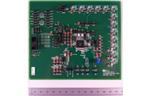
TPS658643 System Evaluation Board
This user’s guide describes the characteristics, operation, and use of the TPS658643EVM-752 evaluation
module (EVM). The TPS658643EVM-752 is a fully assembled and tested platform for evaluating the
performance of the TPS658643 single-chip, power management device. This document includes
schematic diagrams, a printed-circuit board layout, bill of materials, and test data.
1
2
3
4
5
6
7
8
Contents
Introduction .................................................................................................................. 3
1.1
Features ............................................................................................................. 3
1.2
Applications ......................................................................................................... 3
1.3
Requirements ....................................................................................................... 3
Electrical Performance Specifications .................................................................................... 3
Schematic .................................................................................................................... 4
Connector and Test Point Descriptions .................................................................................. 8
4.1
Headers and Switches ............................................................................................ 8
4.2
Jumpers ............................................................................................................. 9
Setup ........................................................................................................................ 10
TPS658643EVM Test Data .............................................................................................. 11
6.1
Operation Waveforms ............................................................................................ 11
EVM Assembly Drawings and Layout .................................................................................. 16
Bill of Materials ............................................................................................................. 20
List of Figures
1
HPA752A Schematic, Sheet 1 ............................................................................................ 4
2
HPA752A Schematic, Sheet 2 ............................................................................................ 5
3
HPA752A Schematic, Sheet 3 ............................................................................................ 6
4
HPA752A Schematic, Sheet 4 ............................................................................................ 7
5
SM0, Ch. 1 - VIN 1 V/div; Ch. 2 - SW 1 V/div; Ch. 3 - Vout 10 mV/div ............................................ 11
6
SM1, Ch. 1 - VIN 1 V/div; Ch. 2 - SW 1 V/div; Ch. 3 - Vout 10 mV/div ............................................ 12
7
SM2, Ch. 1 - VIN 1 V/div; Ch. 2 - SW 1 V/div; Ch. 3 - Vout 10 mV/div ............................................ 12
8
SM0, SM1, SM2, and LDO1 Start-Up
9
LDO1, LDO2, LDO3, and LDO4 Start-Up .............................................................................. 13
10
LDO4, LDO5, and LDO9 Start-Up....................................................................................... 14
11
32-kHz Clock ............................................................................................................... 15
12
Top Assembly – Silkscreen .............................................................................................. 16
13
Top Layer ................................................................................................................... 16
14
Layer 2 ...................................................................................................................... 17
15
Layer 3 ...................................................................................................................... 17
16
Layer 4 ...................................................................................................................... 18
17
Layer 5 ...................................................................................................................... 18
18
Layer 6 ...................................................................................................................... 19
19
Bottom Layer ............................................................................................................... 19
..................................................................................
13
List of Tables
SLVU582A – December 2011 – Revised May 2012
Submit Documentation Feedback
TPS658643 System Evaluation Board
Copyright © 2011–2012, Texas Instruments Incorporated
1
�www.ti.com
1
2
3
2
.....................................................................................................
Jumpers ......................................................................................................................
Bill of Materials.............................................................................................................
Headers and Switches
TPS658643 System Evaluation Board
8
9
20
SLVU582A – December 2011 – Revised May 2012
Submit Documentation Feedback
Copyright © 2011–2012, Texas Instruments Incorporated
�Introduction
www.ti.com
1
Introduction
The TPS658643 is a single-chip, power management integrated circuit (IC) with multiple regulated power
supplies, system management, and display functions in a small package. The I2C interface enables
control of a wide range of subsystem parameters. Internal registers have a complete set of status
information, enabling easy diagnostics and host-controlled handling of fault conditions.
1.1
Features
•
•
•
•
•
•
1.2
Applications
•
•
•
•
•
1.3
Three programmable step-down converters
– Eleven programmable general-purpose LDOs
Three PWM outputs with programmable frequency and duty cycle
Dual RGB LED drivers
Eleven-channel ADC with three operating modes
Power-Good monitoring on all supply outputs
Interrupt controller with maskable interrupts
Tablet Portable Computers
Netbooks
Smart phones
Portable navigation devices
Portable media players
Requirements
In order to operate this EVM properly, the hardware must be connected and properly configured. All
components and connectors are installed on the EVM as shipped, except the dc power supplies.
2
Electrical Performance Specifications
Input voltage, VIN, 3 V to 5.5 V
Output current, step-down converters, 1.5 A (SMO, SM2) and 2 A (SM1)
Output voltage LDOs, seven with output voltages of 1.25 V to 3.3 V, two with output voltages of 0.725 V to
1.5 V, one always on with output voltage of 1.25 V to 3.3 V, one with output voltage of 1.7 V to 2.475 V.
SLVU582A – December 2011 – Revised May 2012
Submit Documentation Feedback
TPS658643 System Evaluation Board
Copyright © 2011–2012, Texas Instruments Incorporated
3
�Schematic
3
www.ti.com
Schematic
Figure 1. HPA752A Schematic, Sheet 1
4
TPS658643 System Evaluation Board
SLVU582A – December 2011 – Revised May 2012
Submit Documentation Feedback
Copyright © 2011–2012, Texas Instruments Incorporated
�Schematic
www.ti.com
Figure 2. HPA752A Schematic, Sheet 2
SLVU582A – December 2011 – Revised May 2012
Submit Documentation Feedback
TPS658643 System Evaluation Board
Copyright © 2011–2012, Texas Instruments Incorporated
5
�Schematic
www.ti.com
Figure 3. HPA752A Schematic, Sheet 3
6
TPS658643 System Evaluation Board
SLVU582A – December 2011 – Revised May 2012
Submit Documentation Feedback
Copyright © 2011–2012, Texas Instruments Incorporated
�Schematic
www.ti.com
Figure 4. HPA752A Schematic, Sheet 4
SLVU582A – December 2011 – Revised May 2012
Submit Documentation Feedback
TPS658643 System Evaluation Board
Copyright © 2011–2012, Texas Instruments Incorporated
7
�Connector and Test Point Descriptions
www.ti.com
4
Connector and Test Point Descriptions
4.1
Headers and Switches
The following table contains header and switch descriptions.
Table 1. Headers and Switches
Header/Switch
8
Title
Description
J1
CHG_DET
Charger Detection Input, connected to CHG_DET (pin D11)
and NC (pins C12,13,D11-13)
J2
PWRGND
Power ground, connected to ground plane
J3
TJ1
Test jumper, connected to VIN pins E13 and F11- 13
J4
PWRGND
Power ground, connected to ground plane
J5
VIN
Power supply input; connect BAT or ac adapter here to J5;
connected to pins A11 - A13, B11 - B13, and C11
J6
PWRGND
Power ground, connected to ground plane
J7
TJ2
Test jumper, connected to VIN pins G10-13
J8
PWRGND
Power ground, connected to ground plane
J9
ADC_IN
Pins COMP (pin N1, input comparator for autoboot feature) and
ALNG1 - ALNG3 (pins L3, M1, M2) - inputs to analog-to-digital
converter. 20-kΩ pulldown to AGND
J10
GPIO
Connected to pins GPIO1 - GPIO4 (M3, M4, N3, N4) with 1-MΩ
pulldown to AGND
J11
USB-I2C ADAPTER
Connection for USB-TO-GPIO TI tool which connects HPA752
board to PC for GUI. Connected to pins GPIO1 - GPIO4 with 1MΩ pulldown to AGND, SAA_3V, SAA_GND, enable for I2C
port expander U2, SCLK ,and SDAT
J12
ADAPTER 3V
Header to sense/supply voltage to I2C bus
J13
SUPERCAP/COINCELL
Header to connect external real-time clock (RTC) supply
J14
32KHZOUT
Header to probe pin OUT32K (C7, pin 1 of J14 is OUT32k and
pin 2 of J14 is analog ground)
J15
AGND
Header with four connections to analog ground to facilitate
oscilloscope ground probe connection
J16
PWM
Header to pin K9; this pin is a no-connect inside the IC (NC6)
J17
DIG_PWM
Header to PWM, digital push-pull output; pin DIG_PWM (N11)
on the IC
J18
DIG_PWM2
Header to PWM, digital push-pull output; pin DIG_PWM2 (F4)
on the IC
J19
SM2
Output of dc/dc converter SM2
J20
PGND2
Power ground 2 for dc/dc converter SM2
J21
SM1
Output of dc/dc converter SM1
J22
PGND1
Power ground 1 for dc/dc converter SM1
J23
SM0
Output of dc/dc converter SM0
J24
PGND0
Power ground 1 for dc/dc converter SM0
J25
DGND2DT_EXTPWR
For IT internal use only
J26
SPARE_OUT
No internal connection
J27
NINT
Header for nINT pin; interruption pin nINT is LO when interrupt
is requested by TPS65864x. Open-drain output
J28
NNORTC
Header for nNORTC pin (D4); output status pin of RTC_OUT
LDO
J29
TNOPWR
Header to monitor NOPOWER pulse width set pin TNOPWR
(A3)
J30
NHOT_RST
Header for nHOT_RST pin (A2); reboot cycle request;
hardware reboot cycle control, pulled up to JP26 (SM2 or 2V2)
through 100 kΩ
J31
NNOPWR
Header for pin nNOPOWER (M11)
J32
RESUME
Header for pin RESUME (B2), connected to switch S3, and
pulled down to DGND through 1 MΩ
J33
SCLK/SDAT
Header for pins SCLK (H4) pin 1 of header and SDAT (J2) pin
2 of header, for monitoring I2C bus
TPS658643 System Evaluation Board
SLVU582A – December 2011 – Revised May 2012
Submit Documentation Feedback
Copyright © 2011–2012, Texas Instruments Incorporated
�Connector and Test Point Descriptions
www.ti.com
Table 1. Headers and Switches (continued)
Header/Switch
4.2
Title
Description
J34
SEQCTRL
Connected to SEQ_CTL pin (B3), pulled down to DGND
through 1MΩ - Discrete input control
J35
LDO4PG
Header for LDO4 Power Good output, pulled down to DGND
through 1MΩ
J36
EVM_3V
Header to connect external supply for LED bias and I2C port
expander U2
J37
SYNCEN
Header for SYNC enable pulled down to DGND through 1MΩ Discrete input control
J38
SM1PG
Header for dc/dc converter SM1 Power Good output
J39
PWRGND
Header for ground connection of external supply for LED bias
and I2C port expander U2
J40
SM1EN
Header for enabling dc/dc converter SM1 pulled down to
DGND through 1MΩ - Discrete input control
J41
SM0PG
Header for dc/dc converter SM0 Power Good output, pulled
down to DGND through 1M-Ohm
J42
SM0EN
Header for enabling dc/dc converter SM0 pulled down to
DGND through 1 MΩ - Discrete input control
J43
AGND
Header with four connections to analog ground
J44
DGND
Header with four connections to digital ground
S1
NOPWRCTL
Assertion of NOPWRCTL assets nNOPOWER output of PMU,
typically used as processor reset without rebooting PMU
S2
NHOT_RST
Used for rebooting PMU
S3
RESUME
Hold to wake up PMU or send PMU to sleep state
Jumpers
The following table shows the installed jumpers.
Table 2. Jumpers
Jumper
Title
Shunt Location
Description
JP1
EXT_THERM
Installed
Jumper to connect thermistor (R2) to pin TS
(J13)
JP2
INT PULLUP
Between pin 1 and pin 2
Jumper to select pullup voltage for INT pin
(L10). Pin 1 and pin 2 shorted INT pulled up
to 2V2. If pin 2 and 3 are shorted /INT is
pulled up to LDO8
JP3
I2C_PU
Not Installed
Jumper to select pullup voltage for SCLK
(H4) and SDAT (J2). Position 1 and position
2 shorted for 2V2 pullup; position 2 and
position 3 shorted for pullup to RTC_OUT
(H1).
JP4
32KOUT-PWR
Installed
Jumper to connect V32K (D7) to RTC_OUT
(H10)
JP5
32K-CLOAD
Not Installed
Jumper to connect 50-pF capacitor to
OUT32K (C7)
JP6
RESUME
Not Installed
Jumper to connect RESUME (B2) to pin P2
of the I2C port expander (U2)
JP7
SEQCTRL
Between pin 1 and pin 2
Jumper to connect SEQCTRL (B3) to either
2V2 or pin P3 of the I2C port expander U2
JP8
SYNCEN
Between pin 1 and pin 2
Jumper to connect SYNCEN (E10) to either
2V2 or pin P4 of the I2C port expander U2
JP9
SM1EN
Between pin 1 and pin 2
Jumper to connect SM1EN (E11) to either
2V2 or pin P5 of the I2C port expander U2
JP10
SM0EN
Not Installed
Jumper to connect SM0EN (F10) to either
2V2 or pin P5 of the I2C port expander U2
JP11
VIN_LDO01
Between pin 2 and pin 3
Jumper to select VIN or SM2 as input to
LDO0 and LDO1
JP12
VIN_LDO23
Between pin 2 and pin 3
Jumper to select VIN or SM2 as input to
LDO2 and LDO3
SLVU582A – December 2011 – Revised May 2012
Submit Documentation Feedback
TPS658643 System Evaluation Board
Copyright © 2011–2012, Texas Instruments Incorporated
9
�Setup
www.ti.com
Table 2. Jumpers (continued)
Jumper
5
Title
Shunt Location
Description
JP13
VIN_LDO4
Between pin 2 and pin 3
Jumper to select VIN or SM2 as input to
LDO4
JP14
VIN_LDO678
Between pin 2 and pin 3
Jumper to select VIN or SM2 as input to
LDO6 - LDO8
JP15
VIN_LDO9
Between pin 2 and pin 3
Jumper to select VIN or SM2 as input to
LDO9
JP16
VIN_SM2
Installed
Jumper to connect VIN to VIN_SM2
JP17
SM2_IL
Installed
Jumper to measure current through inductor
L1
JP18
LED_PWM_DRV
Between pin 2 and pin 3
Jumper to select SM2 or VIN as supply for
LEDs, D14 - D17
JP19
VIN_SM1
Installed
Jumper to connects VIN to VIN_SM1
JP20
SM1_IL
Installed
Jumper to measure current through inductor
L2
JP21
RGB_DRV
Between pin 2 and pin 3
Jumper to select SM2 or VIN as supply for
RGB LED, D18
JP22
VIN_SM0
Installed
Jumper to connects VIN to VIN_SM0
JP23
SM0_IL
Installed
Jumper to measure current through inductor
L3
JP24
RGB2_DRV
Between pin 2 and pin 3
Jumper to select SM2 or VIN as supply for
RGB LED, D19
JP25
DGND2DT
Between pin 2 and pin 3
For TI internal use only
JP26
JP26
Between pin 2 and pin 3
Jumper to select SM2 or 2V2 as pullup for
HOT_RST
JP27
STATUS_LED_PWR
Between pin 1 and pin 2
Jumper to select VIN or EVM_3V J36 as bias
for status LEDs, D1 - D13
Setup
The following steps are intended to help users power up and evaluate the EVM.
1. To use the TPS65864xEVM with a personal computer, the TPS865864xEVM software is required
along with the HPA172 USB-to-I2C Interface Board (USB-TO-GPIO) and a USB cable. Two power
supplies capable of supplying 6 V at 2 A are required.
2. To test the HPA752, the computer must have the TPS65864xEVM software program installed. Install
the program from the TPS65864xEVM software zip file. This software zip file is supplied by Texas
Instruments. If the program does not automatically install properly, follow the instructions in the
Readme file.
3. Connect the USB cable between the computer and the HPA172. Connect the Molex cable between the
HPA172 and the HPA752 EVM (J11).
4. Verify the shorting jumpers are installed as noted in the shorting jumper table. The EVM ships with the
default jumper settings.
5. Supply 1: Set the input supply voltage to 3.3 V before connecting to the EVM, and turn the supply off.
While in the off state, connect the power supply positive lead to J36 (EVM 3V). Connect the power
supply return lead to J39 (GND).
6. Input Supply 2: Set the input supply voltage to 5 V before connecting to the EVM, and turn the supply
off. While in the off state, connect the power supply positive lead to J5 (VIN). Connect the power
supply return lead to J6 (GND).
7. First, turn on Input Supply 1 (3.3 V). Next, turn on Input Supply 2 (5 V).
8. To wake the PMU, hold the pushbutton switch, S1, RESUME, for one seconds and release. While the
PMU is awake, holding switch S1 for one second puts the PMU back into the sleep state. Different
combinations of the LDOs and switching converters turn on by default as per table 3-3: TPS65864x
Integrated Power Supply Power-Up Defaults in the corresponding device data sheet. Note, final silicon
can be marked as TPS658643 or P658643.
9. Using the GUI, select the LDOs tab on the left side. Press Read to load the contents of the I2C
10
TPS658643 System Evaluation Board
SLVU582A – December 2011 – Revised May 2012
Submit Documentation Feedback
Copyright © 2011–2012, Texas Instruments Incorporated
�TPS658643EVM Test Data
www.ti.com
registers into the GUI. Next, check all the unchecked boxes. This enables all the LDOs.
10. Using the GUI, select the SMs tab on the left side. Press Read to load the contents of the I2C
registers into the GUI. Next, check all the unchecked boxes. This enables all the SM converters.
6
TPS658643EVM Test Data
This section presents typical performance data for the TPS658643EVM. Actual performance data can be
affected by measurement techniques and environmental variables; therefore, these results are presented
for reference and may differ from actual results obtained by some users.
6.1
Operation Waveforms
Figure 5. SM0, Ch. 1 - VIN 1 V/div; Ch. 2 - SW 1 V/div; Ch. 3 - Vout 10 mV/div
SLVU582A – December 2011 – Revised May 2012
Submit Documentation Feedback
TPS658643 System Evaluation Board
Copyright © 2011–2012, Texas Instruments Incorporated
11
�TPS658643EVM Test Data
www.ti.com
Figure 6. SM1, Ch. 1 - VIN 1 V/div; Ch. 2 - SW 1 V/div; Ch. 3 - Vout 10 mV/div
Figure 7. SM2, Ch. 1 - VIN 1 V/div; Ch. 2 - SW 1 V/div; Ch. 3 - Vout 10 mV/div
12
TPS658643 System Evaluation Board
SLVU582A – December 2011 – Revised May 2012
Submit Documentation Feedback
Copyright © 2011–2012, Texas Instruments Incorporated
�TPS658643EVM Test Data
www.ti.com
Figure 8. SM0, SM1, SM2, and LDO1 Start-Up
Figure 9. LDO1, LDO2, LDO3, and LDO4 Start-Up
SLVU582A – December 2011 – Revised May 2012
Submit Documentation Feedback
TPS658643 System Evaluation Board
Copyright © 2011–2012, Texas Instruments Incorporated
13
�TPS658643EVM Test Data
www.ti.com
Figure 10. LDO4, LDO5, and LDO9 Start-Up
14
TPS658643 System Evaluation Board
SLVU582A – December 2011 – Revised May 2012
Submit Documentation Feedback
Copyright © 2011–2012, Texas Instruments Incorporated
�TPS658643EVM Test Data
www.ti.com
Figure 11. 32-kHz Clock
SLVU582A – December 2011 – Revised May 2012
Submit Documentation Feedback
TPS658643 System Evaluation Board
Copyright © 2011–2012, Texas Instruments Incorporated
15
�EVM Assembly Drawings and Layout
7
www.ti.com
EVM Assembly Drawings and Layout
TEXAS
INSTRUMENTS
Figure 12. Top Assembly – Silkscreen
Figure 13. Top Layer
16
TPS658643 System Evaluation Board
SLVU582A – December 2011 – Revised May 2012
Submit Documentation Feedback
Copyright © 2011–2012, Texas Instruments Incorporated
�EVM Assembly Drawings and Layout
www.ti.com
Figure 14. Layer 2
Figure 15. Layer 3
SLVU582A – December 2011 – Revised May 2012
Submit Documentation Feedback
TPS658643 System Evaluation Board
Copyright © 2011–2012, Texas Instruments Incorporated
17
�EVM Assembly Drawings and Layout
www.ti.com
Figure 16. Layer 4
Figure 17. Layer 5
18
TPS658643 System Evaluation Board
SLVU582A – December 2011 – Revised May 2012
Submit Documentation Feedback
Copyright © 2011–2012, Texas Instruments Incorporated
�EVM Assembly Drawings and Layout
www.ti.com
Figure 18. Layer 6
Figure 19. Bottom Layer
SLVU582A – December 2011 – Revised May 2012
Submit Documentation Feedback
TPS658643 System Evaluation Board
Copyright © 2011–2012, Texas Instruments Incorporated
19
�Bill of Materials
8
www.ti.com
Bill of Materials
Table 3. Bill of Materials
Count
20
Description
Size
Part Number
MFR
21
RefDes
C1, C2, C4,
10uF
C5, C8, C9,
C10, C11, C12,
C34, C35, C36,
C37, C39, C40,
C41, C42, C43,
C44, C45, C46
Value
Capacitor, Ceramic, 10V, X5R, 10%
0805
GRM21BR61A106KE19L
muRata
1
C13
2200pF
Capacitor, Ceramic, 50V, C0G, 5%
0603
C1608C0G1H222J
TDK
1
C14
6.8uF
Capacitor, Ceramic, 10V, X5R, 10%
0805
C0805C685K8PACTU
Kemet
3
C15, C16, C38
Open
Capacitor, Ceramic
0603
Std
Std
1
C18
50pF
Capacitor, Ceramic, 50V, C0G, 5%
0603
06035A500JAT2A
AVX
1
C3
4.7uF
Capacitor, Ceramic, 10V, X5R, 10%
0805
GRM219R61A475KE19D
muRata
17
C6, C17, C19,
2.2uF
C20, C21, C22,
C23, C24, C25,
C26, C27, C28,
C29, C30, C31,
C32, C33
Capacitor, Ceramic, 10V, X5R, 10%
0603
GRM188R61A225KE34D
muRata
1
C7
Capacitor, Ceramic, 50V, X7R, 10%
0603
C1608X7R1H104K
TDK
13
D1, D2, D3,
LTST-C190GKT
D4, D5, D6,
D7, D8, D9,
D10, D11, D12,
D13
0.1uF
Diode, LED, Green, 2.1V, 10mA, 6mcd
0603
LTST-C190GKT
Lite On
4
D14, D15, D16, LTW-C193TS5
D17
Diode, LED, White, 2.95V, 5mA
0603
LTW-C193TS5
Lite On
2
D18, D19
LATBT66B
Diode, LED, 20mA, Common Anode
0.118 x 0.134
LATBT66B-ST-1+TU735+QS-36-ZB-Z
ALTERNATE: LATBT66B-ST1+TU-35+QR-35-20-R18-ZB
Osram
38
J1, J2, J3, J4,
J5, J6, J7, J8,
J12, J13, J14,
J16, J17, J18,
J19, J20, J21,
J22, J23, J24,
J25, J26, J27,
J28, J29, J30,
J31, J32, J33,
J34, J35, J36,
J37, J38, J39,
J40, J41, J42
PEC02SAAN
Header, 2 pin, 100mil spacing,
0.100 x 2
PEC02SAAN
Sullins
5
J9, J10, J15,
J43, J44
PEC04SAAN
Header, 4 pin, 100mil spacing,
0.100 x 4
PEC04SAAN
Sullins
1
J11
N2510-6002-RB
Connector, Male Straight 2x5 pin, 100mil
spacing, 4 Wall
0.338 x 0.788
N2510-6002-RB
3M
10
JP1, JP4, JP5,
JP6, JP16,
JP17, JP19,
JP20, JP22,
JP23
PEC02SAAN
Header, 2 pin, 100mil spacing,
0.100 x 2
PEC02SAAN
Sullins
17
JP2, JP3, JP7,
JP8, JP9,
JP10, JP11,
JP12, JP13,
JP14, JP15,
JP18, JP21,
JP24, JP25,
JP26, JP27
PEC03SAAN
Header, 3 pin, 100mil spacing,
0.100 x 3
PEC03SAAN
Sullins
1
L1
1.5uH
Inductor, SMT, 3.1A, 78milliohm
0.169 x 0.169 inch
LPS4414-152ML
Coilcraft
2
L2, L3
1.5uH
Inductor, SMT, 2.7A, 70milliohm
0.153 x 0.153 inch
LPS4012-152ML
Coilcraft
6
R1, R19, R20,
R21, R23, R24
10k
Resistor, Chip, 1/16W, 1%
0603
Std
Std
2
R13, R17
0
Resistor, Chip, 1/16W, 1%
0603
Std
Std
TPS658643 System Evaluation Board
SLVU582A – December 2011 – Revised May 2012
Submit Documentation Feedback
Copyright © 2011–2012, Texas Instruments Incorporated
�Bill of Materials
www.ti.com
Table 3. Bill of Materials (continued)
Count
RefDes
Value
Description
Size
Part Number
MFR
1
R18
332
Resistor, Chip, 1/16W, 1%
0603
Std
Std
1
R2
200K
Potentiometer, 1/4 Cermet, 12-Turn, Top- 0.25x0.17
Adjust
3266W-1-204LF
Bourns
Open
1
R22
Resistor, Chip, 1/16W
0603
Std
Std
26
R25, R26, R27, 1.0k
R28, R29, R40,
R41, R42, R43,
R44, R45, R46,
R47, R48, R57,
R58, R59, R60,
R61, R62, R63,
R64, R73, R74,
R75, R76
Resistor, Chip, 1/16W, 1%
0603
Std
Std
4
R3, R89, R90,
R91
100k
Resistor, Chip, 1/16W, 1%
0603
Std
Std
8
R4, R5, R6,
R7, R12, R14,
R15, R16
20k
Resistor, Chip, 1/16W, 1%
0603
Std
Std
1
R77
Open
Resistor, Chip, 1/16W, 1%
0603
Std
Std
4
R78, R79, R80, 100
R81
Resistor, Chip, 1/10W, 1%
0805
Std
Std
39
R8, R9, R10,
1.0M
R11, R30, R31,
R32, R33, R34,
R35, R36, R37,
R38, R39, R49,
R50, R51, R52,
R53, R54, R55,
R56, R65, R66,
R67, R68, R69,
R70, R71, R72,
R88, R92, R93,
R94, R95, R96,
R97, R98, R99
Resistor, Chip, 1/16W, 1%
0603
Std
Std
6
R82, R83, R84, 10
R85, R86, R87
Resistor, Chip, 1/16W, 1%
0603
Std
Std
3
S1, S2, S3
Switch, 1P1T, PB Momentary, 100mA,
SM
0.19 x 0.18 inch
7914G-1-000E
Bourns
38
TP1, TP2, TP3, 5000
TP4, TP5, TP6,
TP7, TP8, TP9,
TP10, TP11,
TP12, TP13,
TP14, TP15,
TP16, TP17,
TP18, TP19,
TP20, TP26,
TP27, TP28,
TP29, TP30,
TP31, TP32,
TP33, TP38,
TP39, TP44,
TP46, TP48,
TP51, TP54,
TP56, TP58,
TP61
Test Point, Red, Thru Hole Color Keyed
0.100 x 0.100 inch
5000
Keystone
20
TP21,
TP23,
TP25,
TP35,
TP37,
TP42,
TP47,
TP52,
TP55,
TP59,
TP22,
TP24,
TP34,
TP36,
TP40,
TP45,
TP49,
TP53,
TP57,
TP60
5001
Test Point, Black, Thru Hole Color Keyed
0.100 x 0.100 inch
5001
Keystone
3
TP41, TP43,
TP50
5002
Test Point, White, Thru Hole Color Keyed 0.100 x 0.100 inch
5002
Keystone
1
U1
TPS658643ZGU
IC, Advanced Power Management Unit
TPS658643ZGU
TI
7914G-1-000E
SLVU582A – December 2011 – Revised May 2012
Submit Documentation Feedback
BGA
TPS658643 System Evaluation Board
Copyright © 2011–2012, Texas Instruments Incorporated
21
�Bill of Materials
www.ti.com
Table 3. Bill of Materials (continued)
Count
22
RefDes
Value
Description
Size
Part Number
MFR
1
U2
PCF8574ADW
IC, Remote 8-Bit I/O Expander For I2C
Bus
SO-16
PCF8574ADW
TI
13
U3, U4, U5,
TLV3011AIDCK
U6, U7, U8,
U9, U10, U11,
U12, U13, U14,
U15
IC, Nanopower, 1.8V, Open-Drain
Comparator With Reference
SC70-6
TLV3011AIDCK
TI
1
Y1
Crystal, 32.768MHz, 12.5pF Capacitance
1.5mm x 3.2mm
CM315-32.768KDZF-UT
Citizen
1
--
PCB, 5.8 In x 5 In x 0.062 In
HPA752
Any
27
--
Shunt, 100-mil, Black
929950-00
3M
32.768KHz
TPS658643 System Evaluation Board
0.100
SLVU582A – December 2011 – Revised May 2012
Submit Documentation Feedback
Copyright © 2011–2012, Texas Instruments Incorporated
�EVALUATION BOARD/KIT/MODULE (EVM) ADDITIONAL TERMS
Texas Instruments (TI) provides the enclosed Evaluation Board/Kit/Module (EVM) under the following conditions:
The user assumes all responsibility and liability for proper and safe handling of the goods. Further, the user indemnifies TI from all claims
arising from the handling or use of the goods.
Should this evaluation board/kit not meet the specifications indicated in the User’s Guide, the board/kit may be returned within 30 days from
the date of delivery for a full refund. THE FOREGOING LIMITED WARRANTY IS THE EXCLUSIVE WARRANTY MADE BY SELLER TO
BUYER AND IS IN LIEU OF ALL OTHER WARRANTIES, EXPRESSED, IMPLIED, OR STATUTORY, INCLUDING ANY WARRANTY OF
MERCHANTABILITY OR FITNESS FOR ANY PARTICULAR PURPOSE. EXCEPT TO THE EXTENT OF THE INDEMNITY SET FORTH
ABOVE, NEITHER PARTY SHALL BE LIABLE TO THE OTHER FOR ANY INDIRECT, SPECIAL, INCIDENTAL, OR CONSEQUENTIAL
DAMAGES.
Please read the User's Guide and, specifically, the Warnings and Restrictions notice in the User's Guide prior to handling the product. This
notice contains important safety information about temperatures and voltages. For additional information on TI's environmental and/or safety
programs, please visit www.ti.com/esh or contact TI.
No license is granted under any patent right or other intellectual property right of TI covering or relating to any machine, process, or
combination in which such TI products or services might be or are used. TI currently deals with a variety of customers for products, and
therefore our arrangement with the user is not exclusive. TI assumes no liability for applications assistance, customer product design,
software performance, or infringement of patents or services described herein.
REGULATORY COMPLIANCE INFORMATION
As noted in the EVM User’s Guide and/or EVM itself, this EVM and/or accompanying hardware may or may not be subject to the Federal
Communications Commission (FCC) and Industry Canada (IC) rules.
For EVMs not subject to the above rules, this evaluation board/kit/module is intended for use for ENGINEERING DEVELOPMENT,
DEMONSTRATION OR EVALUATION PURPOSES ONLY and is not considered by TI to be a finished end product fit for general consumer
use. It generates, uses, and can radiate radio frequency energy and has not been tested for compliance with the limits of computing
devices pursuant to part 15 of FCC or ICES-003 rules, which are designed to provide reasonable protection against radio frequency
interference. Operation of the equipment may cause interference with radio communications, in which case the user at his own expense will
be required to take whatever measures may be required to correct this interference.
General Statement for EVMs including a radio
User Power/Frequency Use Obligations: This radio is intended for development/professional use only in legally allocated frequency and
power limits. Any use of radio frequencies and/or power availability of this EVM and its development application(s) must comply with local
laws governing radio spectrum allocation and power limits for this evaluation module. It is the user’s sole responsibility to only operate this
radio in legally acceptable frequency space and within legally mandated power limitations. Any exceptions to this are strictly prohibited and
unauthorized by Texas Instruments unless user has obtained appropriate experimental/development licenses from local regulatory
authorities, which is responsibility of user including its acceptable authorization.
For EVMs annotated as FCC – FEDERAL COMMUNICATIONS COMMISSION Part 15 Compliant
Caution
This device complies with part 15 of the FCC Rules. Operation is subject to the following two conditions: (1) This device may not cause
harmful interference, and (2) this device must accept any interference received, including interference that may cause undesired operation.
Changes or modifications not expressly approved by the party responsible for compliance could void the user's authority to operate the
equipment.
FCC Interference Statement for Class A EVM devices
This equipment has been tested and found to comply with the limits for a Class A digital device, pursuant to part 15 of the FCC Rules.
These limits are designed to provide reasonable protection against harmful interference when the equipment is operated in a commercial
environment. This equipment generates, uses, and can radiate radio frequency energy and, if not installed and used in accordance with the
instruction manual, may cause harmful interference to radio communications. Operation of this equipment in a residential area is likely to
cause harmful interference in which case the user will be required to correct the interference at his own expense.
�FCC Interference Statement for Class B EVM devices
This equipment has been tested and found to comply with the limits for a Class B digital device, pursuant to part 15 of the FCC Rules.
These limits are designed to provide reasonable protection against harmful interference in a residential installation. This equipment
generates, uses and can radiate radio frequency energy and, if not installed and used in accordance with the instructions, may cause
harmful interference to radio communications. However, there is no guarantee that interference will not occur in a particular installation. If
this equipment does cause harmful interference to radio or television reception, which can be determined by turning the equipment off and
on, the user is encouraged to try to correct the interference by one or more of the following measures:
• Reorient or relocate the receiving antenna.
• Increase the separation between the equipment and receiver.
• Connect the equipment into an outlet on a circuit different from that to which the receiver is connected.
• Consult the dealer or an experienced radio/TV technician for help.
For EVMs annotated as IC – INDUSTRY CANADA Compliant
This Class A or B digital apparatus complies with Canadian ICES-003.
Changes or modifications not expressly approved by the party responsible for compliance could void the user’s authority to operate the
equipment.
Concerning EVMs including radio transmitters
This device complies with Industry Canada licence-exempt RSS standard(s). Operation is subject to the following two conditions: (1) this
device may not cause interference, and (2) this device must accept any interference, including interference that may cause undesired
operation of the device.
Concerning EVMs including detachable antennas
Under Industry Canada regulations, this radio transmitter may only operate using an antenna of a type and maximum (or lesser) gain
approved for the transmitter by Industry Canada. To reduce potential radio interference to other users, the antenna type and its gain should
be so chosen that the equivalent isotropically radiated power (e.i.r.p.) is not more than that necessary for successful communication.
This radio transmitter has been approved by Industry Canada to operate with the antenna types listed in the user guide with the maximum
permissible gain and required antenna impedance for each antenna type indicated. Antenna types not included in this list, having a gain
greater than the maximum gain indicated for that type, are strictly prohibited for use with this device.
Cet appareil numérique de la classe A ou B est conforme à la norme NMB-003 du Canada.
Les changements ou les modifications pas expressément approuvés par la partie responsable de la conformité ont pu vider l’autorité de
l'utilisateur pour actionner l'équipement.
Concernant les EVMs avec appareils radio
Le présent appareil est conforme aux CNR d'Industrie Canada applicables aux appareils radio exempts de licence. L'exploitation est
autorisée aux deux conditions suivantes : (1) l'appareil ne doit pas produire de brouillage, et (2) l'utilisateur de l'appareil doit accepter tout
brouillage radioélectrique subi, même si le brouillage est susceptible d'en compromettre le fonctionnement.
Concernant les EVMs avec antennes détachables
Conformément à la réglementation d'Industrie Canada, le présent émetteur radio peut fonctionner avec une antenne d'un type et d'un gain
maximal (ou inférieur) approuvé pour l'émetteur par Industrie Canada. Dans le but de réduire les risques de brouillage radioélectrique à
l'intention des autres utilisateurs, il faut choisir le type d'antenne et son gain de sorte que la puissance isotrope rayonnée équivalente
(p.i.r.e.) ne dépasse pas l'intensité nécessaire à l'établissement d'une communication satisfaisante.
Le présent émetteur radio a été approuvé par Industrie Canada pour fonctionner avec les types d'antenne énumérés dans le manuel
d’usage et ayant un gain admissible maximal et l'impédance requise pour chaque type d'antenne. Les types d'antenne non inclus dans
cette liste, ou dont le gain est supérieur au gain maximal indiqué, sont strictement interdits pour l'exploitation de l'émetteur.
SPACER
SPACER
SPACER
SPACER
SPACER
SPACER
SPACER
SPACER
�【Important Notice for Users of this Product in Japan】
】
This development kit is NOT certified as Confirming to Technical Regulations of Radio Law of Japan
If you use this product in Japan, you are required by Radio Law of Japan to follow the instructions below with respect to this product:
1.
2.
3.
Use this product in a shielded room or any other test facility as defined in the notification #173 issued by Ministry of Internal Affairs and
Communications on March 28, 2006, based on Sub-section 1.1 of Article 6 of the Ministry’s Rule for Enforcement of Radio Law of
Japan,
Use this product only after you obtained the license of Test Radio Station as provided in Radio Law of Japan with respect to this
product, or
Use of this product only after you obtained the Technical Regulations Conformity Certification as provided in Radio Law of Japan with
respect to this product. Also, please do not transfer this product, unless you give the same notice above to the transferee. Please note
that if you could not follow the instructions above, you will be subject to penalties of Radio Law of Japan.
Texas Instruments Japan Limited
(address) 24-1, Nishi-Shinjuku 6 chome, Shinjuku-ku, Tokyo, Japan
http://www.tij.co.jp
【ご使用にあたっての注】
本開発キットは技術基準適合証明を受けておりません。
本製品のご使用に際しては、電波法遵守のため、以下のいずれかの措置を取っていただく必要がありますのでご注意ください。
1.
2.
3.
電波法施行規則第6条第1項第1号に基づく平成18年3月28日総務省告示第173号で定められた電波暗室等の試験設備でご使用いただく。
実験局の免許を取得後ご使用いただく。
技術基準適合証明を取得後ご使用いただく。
なお、本製品は、上記の「ご使用にあたっての注意」を譲渡先、移転先に通知しない限り、譲渡、移転できないものとします。
上記を遵守頂けない場合は、電波法の罰則が適用される可能性があることをご留意ください。
日本テキサス・インスツルメンツ株式会社
東京都新宿区西新宿6丁目24番1号
西新宿三井ビル
http://www.tij.co.jp
SPACER
SPACER
SPACER
SPACER
SPACER
SPACER
SPACER
SPACER
SPACER
SPACER
SPACER
SPACER
SPACER
SPACER
SPACER
SPACER
�EVALUATION BOARD/KIT/MODULE (EVM)
WARNINGS, RESTRICTIONS AND DISCLAIMERS
For Feasibility Evaluation Only, in Laboratory/Development Environments. Unless otherwise indicated, this EVM is not a finished
electrical equipment and not intended for consumer use. It is intended solely for use for preliminary feasibility evaluation in
laboratory/development environments by technically qualified electronics experts who are familiar with the dangers and application risks
associated with handling electrical mechanical components, systems and subsystems. It should not be used as all or part of a finished end
product.
Your Sole Responsibility and Risk. You acknowledge, represent and agree that:
1.
2.
3.
4.
You have unique knowledge concerning Federal, State and local regulatory requirements (including but not limited to Food and Drug
Administration regulations, if applicable) which relate to your products and which relate to your use (and/or that of your employees,
affiliates, contractors or designees) of the EVM for evaluation, testing and other purposes.
You have full and exclusive responsibility to assure the safety and compliance of your products with all such laws and other applicable
regulatory requirements, and also to assure the safety of any activities to be conducted by you and/or your employees, affiliates,
contractors or designees, using the EVM. Further, you are responsible to assure that any interfaces (electronic and/or mechanical)
between the EVM and any human body are designed with suitable isolation and means to safely limit accessible leakage currents to
minimize the risk of electrical shock hazard.
You will employ reasonable safeguards to ensure that your use of the EVM will not result in any property damage, injury or death, even
if the EVM should fail to perform as described or expected.
You will take care of proper disposal and recycling of the EVM’s electronic components and packing materials.
Certain Instructions. It is important to operate this EVM within TI’s recommended specifications and environmental considerations per the
user guidelines. Exceeding the specified EVM ratings (including but not limited to input and output voltage, current, power, and
environmental ranges) may cause property damage, personal injury or death. If there are questions concerning these ratings please contact
a TI field representative prior to connecting interface electronics including input power and intended loads. Any loads applied outside of the
specified output range may result in unintended and/or inaccurate operation and/or possible permanent damage to the EVM and/or
interface electronics. Please consult the EVM User's Guide prior to connecting any load to the EVM output. If there is uncertainty as to the
load specification, please contact a TI field representative. During normal operation, some circuit components may have case temperatures
greater than 60°C as long as the input and output are maintained at a normal ambient operating temperature. These components include
but are not limited to linear regulators, switching transistors, pass transistors, and current sense resistors which can be identified using the
EVM schematic located in the EVM User's Guide. When placing measurement probes near these devices during normal operation, please
be aware that these devices may be very warm to the touch. As with all electronic evaluation tools, only qualified personnel knowledgeable
in electronic measurement and diagnostics normally found in development environments should use these EVMs.
Agreement to Defend, Indemnify and Hold Harmless. You agree to defend, indemnify and hold TI, its licensors and their representatives
harmless from and against any and all claims, damages, losses, expenses, costs and liabilities (collectively, "Claims") arising out of or in
connection with any use of the EVM that is not in accordance with the terms of the agreement. This obligation shall apply whether Claims
arise under law of tort or contract or any other legal theory, and even if the EVM fails to perform as described or expected.
Safety-Critical or Life-Critical Applications. If you intend to evaluate the components for possible use in safety critical applications (such
as life support) where a failure of the TI product would reasonably be expected to cause severe personal injury or death, such as devices
which are classified as FDA Class III or similar classification, then you must specifically notify TI of such intent and enter into a separate
Assurance and Indemnity Agreement.
Mailing Address: Texas Instruments, Post Office Box 655303, Dallas, Texas 75265
Copyright © 2012, Texas Instruments Incorporated
�IMPORTANT NOTICE
Texas Instruments Incorporated and its subsidiaries (TI) reserve the right to make corrections, modifications, enhancements, improvements,
and other changes to its products and services at any time and to discontinue any product or service without notice. Customers should
obtain the latest relevant information before placing orders and should verify that such information is current and complete. All products are
sold subject to TI’s terms and conditions of sale supplied at the time of order acknowledgment.
TI warrants performance of its hardware products to the specifications applicable at the time of sale in accordance with TI’s standard
warranty. Testing and other quality control techniques are used to the extent TI deems necessary to support this warranty. Except where
mandated by government requirements, testing of all parameters of each product is not necessarily performed.
TI assumes no liability for applications assistance or customer product design. Customers are responsible for their products and
applications using TI components. To minimize the risks associated with customer products and applications, customers should provide
adequate design and operating safeguards.
TI does not warrant or represent that any license, either express or implied, is granted under any TI patent right, copyright, mask work right,
or other TI intellectual property right relating to any combination, machine, or process in which TI products or services are used. Information
published by TI regarding third-party products or services does not constitute a license from TI to use such products or services or a
warranty or endorsement thereof. Use of such information may require a license from a third party under the patents or other intellectual
property of the third party, or a license from TI under the patents or other intellectual property of TI.
Reproduction of TI information in TI data books or data sheets is permissible only if reproduction is without alteration and is accompanied
by all associated warranties, conditions, limitations, and notices. Reproduction of this information with alteration is an unfair and deceptive
business practice. TI is not responsible or liable for such altered documentation. Information of third parties may be subject to additional
restrictions.
Resale of TI products or services with statements different from or beyond the parameters stated by TI for that product or service voids all
express and any implied warranties for the associated TI product or service and is an unfair and deceptive business practice. TI is not
responsible or liable for any such statements.
TI products are not authorized for use in safety-critical applications (such as life support) where a failure of the TI product would reasonably
be expected to cause severe personal injury or death, unless officers of the parties have executed an agreement specifically governing
such use. Buyers represent that they have all necessary expertise in the safety and regulatory ramifications of their applications, and
acknowledge and agree that they are solely responsible for all legal, regulatory and safety-related requirements concerning their products
and any use of TI products in such safety-critical applications, notwithstanding any applications-related information or support that may be
provided by TI. Further, Buyers must fully indemnify TI and its representatives against any damages arising out of the use of TI products in
such safety-critical applications.
TI products are neither designed nor intended for use in military/aerospace applications or environments unless the TI products are
specifically designated by TI as military-grade or "enhanced plastic." Only products designated by TI as military-grade meet military
specifications. Buyers acknowledge and agree that any such use of TI products which TI has not designated as military-grade is solely at
the Buyer's risk, and that they are solely responsible for compliance with all legal and regulatory requirements in connection with such use.
TI products are neither designed nor intended for use in automotive applications or environments unless the specific TI products are
designated by TI as compliant with ISO/TS 16949 requirements. Buyers acknowledge and agree that, if they use any non-designated
products in automotive applications, TI will not be responsible for any failure to meet such requirements.
Following are URLs where you can obtain information on other Texas Instruments products and application solutions:
Products
Applications
Audio
www.ti.com/audio
Automotive and Transportation www.ti.com/automotive
Amplifiers
amplifier.ti.com
Communications and Telecom www.ti.com/communications
Data Converters
dataconverter.ti.com
Computers and Peripherals
www.ti.com/computers
DLP® Products
www.dlp.com
Consumer Electronics
www.ti.com/consumer-apps
DSP
dsp.ti.com
Energy and Lighting
www.ti.com/energy
Clocks and Timers
www.ti.com/clocks
Industrial
www.ti.com/industrial
Interface
interface.ti.com
Medical
www.ti.com/medical
Logic
logic.ti.com
Security
www.ti.com/security
Power Mgmt
power.ti.com
Space, Avionics and Defense
www.ti.com/space-avionics-defense
Microcontrollers
microcontroller.ti.com
Video and Imaging
www.ti.com/video
RFID
www.ti-rfid.com
OMAP Mobile Processors
www.ti.com/omap
Wireless Connectivity
www.ti.com/wirelessconnectivity
TI E2E Community Home Page
e2e.ti.com
Mailing Address: Texas Instruments, Post Office Box 655303, Dallas, Texas 75265
Copyright © 2012, Texas Instruments Incorporated
�