www.ti.com
User’s Guide
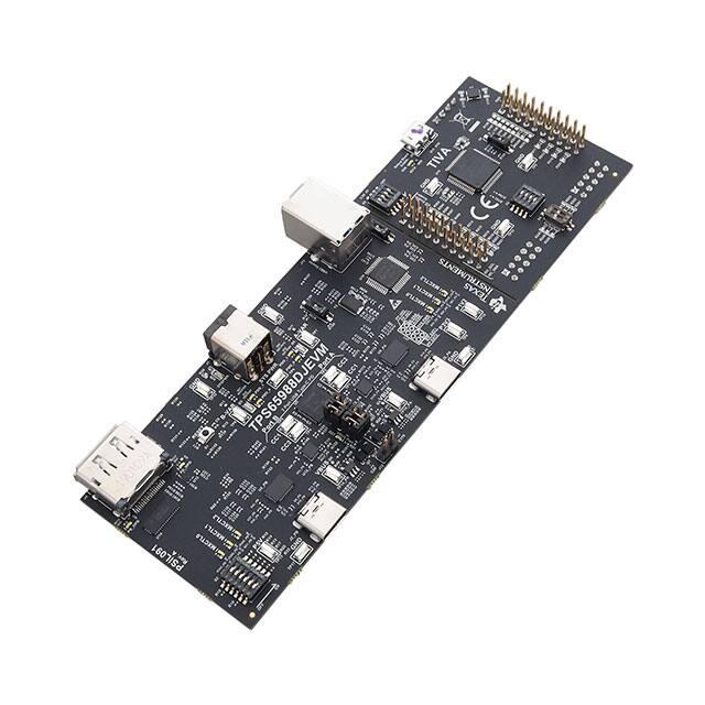
TPS65988 Evaluation Module
ABSTRACT
This document is the user guide for the TPS65988 Evaluation Module (TPS65988EVM). The TPS65988EVM
allows for evaluation of the TPS65988 IC as part of a stand-alone testing kit and for development and testing of
USB Type-C and Power Delivery (PD) end products. Out of the box, the TPS65988EVM is configured to emulate
a dual-port laptop computer. Both ports can be used to source or sink power, and both are dual-role ports (DRP)
but only support data as a downstream-facing port (DFP) host. When different configurations are required to test
your system, use the TPS65988 Application Configuration software tool to create a configuration or load a
different configuration template (see Figure 1-1). The TPS65988EVM uses a control MUX (HD3SS3412) to route
DisplayPort™ (DP) and a USB HUB (TUSB8020) to route USB signals to the appropriate port A or port A (port
A/B). The control MUX and USB HUB are connected to a SuperSpeed (SS) MUX (TUSB546) which routes the
appropriate DP lanes and USB 3.0 signals according to cable orientation and Alternate Mode selection. Figure
1-2 highlights these features.
Figure 1-1. TPS65988EVM
SLVUB62B – JUNE 2017 – REVISED NOVEMBER 2020
Submit Document Feedback
Copyright © 2020 Texas Instruments Incorporated
TPS65988 Evaluation Module
1
�www.ti.com
Table of Contents
C_SSTX
/RX
I2C
TUSB546
MUX_CTR
L0-2
AUX
DP0-3
DP
source
USB2
USB
source
USB3
PFET Control
PPEXT1
Sink
C_SSTX/RX
GPIO
PP1_CABLE
USB2.0
BC1.2
PPHV
1
VBUS1
CC1/2
System 5V
5/9/15/20V @3A
Variable DC/DC
C1_CC1/2
I2C1
I2C2
Port A
TPS65988
System Power (20V) DC
Barrel Jack
System 3.3V
VIN_3V3
Type C
Receptacle
Port B
PPHV2
VBUS2
C2_CC1/2
BC1.2
USB2.0
C_SSTX/RX
PPEXT2
CC1/2
5/9/15/20V @3A
Variable DC/DC
PP2_CABLE
System 5V
GPIO
Sink
PFET Control
MUX_CTR
L0-2
I2C
TUSB546
C_SSTX
/RX
AUX
DP0-3
DP
source
USB2
USB
source
USB3
Copyright © 2017, Texas Instruments Incorporated
Figure 1-2. TPS65988EVM Block Diagram
Table of Contents
1 About this Manual...................................................................................................................................................................5
2 Information About Cautions and Warnings..........................................................................................................................5
3 Items Required for Operation................................................................................................................................................ 5
4 Introduction.............................................................................................................................................................................5
5 Setup........................................................................................................................................................................................6
5.1 Switch, Push Button, Connector, and Test Point Descriptions........................................................................................... 6
5.2 LED Indicators Description...............................................................................................................................................25
2
TPS65988 Evaluation Module
SLVUB62B – JUNE 2017 – REVISED NOVEMBER 2020
Submit Document Feedback
Copyright © 2020 Texas Instruments Incorporated
�Table of Contents
www.ti.com
6 Using the TPS65988EVM......................................................................................................................................................29
6.1 Powering the TPS65988EVM.......................................................................................................................................... 29
6.2 Firmware Configurations.................................................................................................................................................. 29
7 Connecting the EVM.............................................................................................................................................................30
7.1 Connecting to Various Devices........................................................................................................................................ 30
7.2 Debugging the EVM......................................................................................................................................................... 35
8 REACH Compliance..............................................................................................................................................................37
9 TPS65988EVM Schematic.................................................................................................................................................... 38
10 TPS65988EVM Board Layout.............................................................................................................................................51
11 TPS65988EVM Bill of Materials..........................................................................................................................................54
12 Revision History................................................................................................................................................................. 62
List of Figures
Figure 1-1. TPS65988EVM..........................................................................................................................................................1
Figure 1-2. TPS65988EVM Block Diagram................................................................................................................................. 2
Figure 5-1. TPS65988 Jumper Configuration.............................................................................................................................. 7
Figure 5-2. TPS65988 Jumper Configuration Net Names........................................................................................................... 7
Figure 5-3. TPS65987D Jumper Configuration........................................................................................................................... 8
Figure 5-4. TPS65987D Jumper Configuration Net Names........................................................................................................ 8
Figure 5-5. TPS65987S Jumper Configuration............................................................................................................................9
Figure 5-6. TPS65987S Jumper Configuration Net Names.......................................................................................................10
Figure 5-7. DisplayPort Source Schematic Block...................................................................................................................... 10
Figure 5-8. DisplayPort Source Block Diagram......................................................................................................................... 10
Figure 5-9. DisplayPort Source Receptacle............................................................................................................................... 11
Figure 5-10. HRESET Push-Button (S1) Schematic..................................................................................................................11
Figure 5-11. HRESET Push-Button (S1)....................................................................................................................................11
Figure 5-12. SPI-MISO Pull Down Switch................................................................................................................................. 12
Figure 5-13. FTDI Dip Switch (S3) Schematic...........................................................................................................................12
Figure 5-14. FTDI Dip Switch (S3).............................................................................................................................................13
Figure 5-15. I2C and BusPower DIP Switch (S2)...................................................................................................................... 14
Figure 5-16. I2C DIP Switch (S2) Schematic.............................................................................................................................14
Figure 5-17. Barrel Jack (J1) Schematic................................................................................................................................... 15
Figure 5-18. Barrel Jack (J1)..................................................................................................................................................... 15
Figure 5-19. Barrel Jack Detect Schematic............................................................................................................................... 16
Figure 5-20. USB Type-B Receptacle (J11) Schematic............................................................................................................. 16
Figure 5-21. USB (J11) Block Diagram......................................................................................................................................16
Figure 5-22. USB Type-B Receptacle (J11)...............................................................................................................................17
Figure 5-23. USB Type-C Receptacles (J2) Schematic.............................................................................................................18
Figure 5-24. USB Type-C Receptacles (J2).............................................................................................................................. 18
Figure 5-25. USB Micro-B Receptacle (J9) Schematic..............................................................................................................19
Figure 5-26. USB Micro-B Receptacle (J9)............................................................................................................................... 19
Figure 5-27. TP13 (5 V), TP8 (3.3 V), and TP12 (1.2 V)........................................................................................................... 20
Figure 5-28. Aardvark Connector (J10) Schematic................................................................................................................... 21
Figure 5-29. Aardvark Connector (J10)..................................................................................................................................... 21
Figure 5-30. TP10, TP11, TP15, TP16, TP17, TP18, TP9: GND Test Points............................................................................ 21
Figure 5-31. TP1, TP2, TP3 and TP4 – CC1 and CC2 Test Points........................................................................................... 22
Figure 5-32. TPS65988 BMC Data............................................................................................................................................22
Figure 5-33. VBUS Test Points: TP14....................................................................................................................................... 23
Figure 5-34. TPS65988 VBUS Voltage Transition..................................................................................................................... 23
Figure 5-35. A-Var, B-Var and System Power Test Points: TP7, TP6, and TP5........................................................................ 24
Figure 5-36. BoosterPack Headers (J3 and J4)........................................................................................................................ 25
Figure 5-37. MUX Control LEDs................................................................................................................................................ 26
Figure 5-38. HPD Port A/B LEDs...............................................................................................................................................26
Figure 5-39. PDO Port A/B LEDs.............................................................................................................................................. 27
Figure 7-1. Connecting EVM to Type-A Device......................................................................................................................... 30
Figure 7-2. Connecting EVM to USB Type-C Devices...............................................................................................................31
Figure 7-3. DRP CC1 and CC2 Toggling................................................................................................................................... 35
Figure 7-4. USB Type-C Connection and VBUS....................................................................................................................... 35
Figure 7-5. USB Type-C Connection and PD Negotiation......................................................................................................... 36
Figure 9-1. TPS65988EVM Block Diagram............................................................................................................................... 38
Figure 9-2. TPS65988EVM Processor Block.............................................................................................................................39
Figure 9-3. TPS65988EVM Power Path Block.......................................................................................................................... 40
Figure 9-4. TPS65988EVM Power Supply Block.......................................................................................................................41
SLVUB62B – JUNE 2017 – REVISED NOVEMBER 2020
Submit Document Feedback
Copyright © 2020 Texas Instruments Incorporated
TPS65988 Evaluation Module
3
�Trademarks
www.ti.com
Figure 9-5. TPS65988EVM DisplayPort Mux............................................................................................................................ 42
Figure 9-6. TPS65988EVM SS MUX Block Port A ................................................................................................................... 43
Figure 9-7. TPS65988EVM SS MUX Block Port B.................................................................................................................... 44
Figure 9-8. TPS65988EVM USB HUB.......................................................................................................................................45
Figure 9-9. TPS65988EVM USB Type-C Port-A Block .............................................................................................................46
Figure 9-10. TPS65988EVM USB Type-C Port B Block ...........................................................................................................47
Figure 9-11. TPS65988EVM FTDI Connector Block..................................................................................................................48
Figure 9-12. TPS65988EVM Current Sense Block Port A.........................................................................................................49
Figure 9-13. TPS65988EVM Current Sense Block Port B.........................................................................................................49
Figure 9-14. TPS65988EVM BoosterPack Header Block..........................................................................................................50
Figure 10-1. TPS65988EVM Top Overlay................................................................................................................................. 51
Figure 10-2. TPS65988EVM Solder.......................................................................................................................................... 51
Figure 10-3. TPS65988EVM Top Layer SSTXRX1................................................................................................................... 51
Figure 10-4. TPS65988EVM GND Plane 1............................................................................................................................... 51
Figure 10-5. TPS65988EVM High Speed..................................................................................................................................52
Figure 10-6. TPS65988EVM GND Plane 2............................................................................................................................... 52
Figure 10-7. TPS65988EVM Power 1....................................................................................................................................... 52
Figure 10-8. TPS65988EVM Power 2....................................................................................................................................... 52
Figure 10-9. TPS65988EVM GND Plane 3............................................................................................................................... 53
Figure 10-10. TPS65988EVM SSTXRX2.................................................................................................................................. 53
Figure 10-11. TPS65988EVM Solder Mask............................................................................................................................... 53
Figure 10-12. TPS65988EVM Bottom Layer Component View................................................................................................. 53
List of Tables
Table 5-1. Port A SS MUX Control LED Functions.................................................................................................................... 26
Table 5-2. Port B SS MUX Control LED Functions.................................................................................................................... 27
Table 5-3. Variable DC/DC Control Port A/B Functions............................................................................................................. 27
Table 5-4. PDO LED 0 and PDO LED 1 Truth Table..................................................................................................................28
Table 5-5. I2C Address Setting.................................................................................................................................................. 28
Table 5-6. ADCIN1 Setting.........................................................................................................................................................28
Table 7-1. DisplayPort and USB Test Setup.............................................................................................................................. 33
Table 8-1. REACH Compliance................................................................................................................................................. 37
Table 11-1. TPS65988EVM Bill of Materials.............................................................................................................................. 54
Trademarks
USB Type-C™ are trademarks of USB Implementers Forum.
Aardvark™ are trademarks of Total Phase, Incorporated.
DisplayPort™ are trademarks of Video Electronics Standards Association.
BoosterPack™ is a trademark of Texas Instruments.
FTDI® and Future Technology Devices International®, are registered trademarks of Future Technology Devices
International Limited.
Dell® is a registered trademark of Dell Incorporated.
Total Phase® is a registered trademark of Total Phase, Incorporated.
Microsoft® and Windows® are registered trademarks of Microsoft Corporation.
All trademarks are the property of their respective owners.
4
TPS65988 Evaluation Module
SLVUB62B – JUNE 2017 – REVISED NOVEMBER 2020
Submit Document Feedback
Copyright © 2020 Texas Instruments Incorporated
�About this Manual
www.ti.com
1 About this Manual
This user's guide describes the TPS65988EVM. The guide consists of an introduction, setup instructions, the
EVM schematic, board layouts, component views, internal power (PWR) and ground (GND) plane layouts, and a
bill of materials (BOM).
2 Information About Cautions and Warnings
ATTENTION
STATIC SENSITIVE DEVICES
HANDLE ONLY AT
STATIC SAFE WORK STATIONS
CAUTION
This EVM contains components that can potentially be damaged by electrostatic discharge. Always
transport and store the EVM in the supplied ESD bag when not in use. Handle using an antistatic
wristband. Operate on an antistatic work surface. For more information on proper handling, see
Electrostatic Discharge (ESD).
3 Items Required for Operation
The following items are required to use the TPS65988EVM:
•
•
•
•
•
•
•
•
•
TPS65988 data sheet
TPS65988EVM
TPS65988 Application Customization Tool
20-V barrel jack adapter or DC power supply (model # 492-BBGP)
Passive USB Type-C™ cables
USB Type-A to USB Micro-B cable
USB Type-A to USB Type-B cable
Mini-DisplayPort to DisplayPort cables
Notebook with USB 2.0, USB 3.0, and DP capabilities
4 Introduction
The TPS65988 is a stand-alone USB Type-C and Power Delivery (PD) controller providing cable plug and
orientation detection at the USB Type-C connector. Upon cable plug and orientation detection, the TPS65988
communicates on the CC line using the USB PD protocol. When cable detection and USB PD negotiation are
complete, the TPS65988 enables the appropriate power path and configures external multiplexers and alternate
mode settings.
This user guide describes how the TPS65988EVM can be used to test DisplayPort alternate mode as well as
USB Data. This guide also contains testing procedures of DP alternate mode as well as various PD power
configurations. The EVM is customizable through the TPS65988 Configuration Tool. Additionally, the EVM is
equipped with a Future Technology Devices International® ( FTDI®) board and Aardvark connector to SPI or I2C
interfaces for debugging and development.
SLVUB62B – JUNE 2017 – REVISED NOVEMBER 2020
Submit Document Feedback
Copyright © 2020 Texas Instruments Incorporated
TPS65988 Evaluation Module
5
�Setup
www.ti.com
5 Setup
This section describes the various EVM features and how to test these features. Schematic screen shots,
pictures, and block diagrams are provided as necessary.
5.1 Switch, Push Button, Connector, and Test Point Descriptions
Components described in this section are listed with respect to the EVM from left to right and top to bottom.
Related components are listed simultaneously.
5.1.1 Power Path Jumper Configuration
The TPS65988EVM allows for analysis of TPS65987D and TPS65987S platforms through the adjustment of
jumpers on J11 and J12.
6
TPS65988 Evaluation Module
SLVUB62B – JUNE 2017 – REVISED NOVEMBER 2020
Submit Document Feedback
Copyright © 2020 Texas Instruments Incorporated
�Setup
www.ti.com
5.1.1.1 TPS65988 Jumper Configuration
Out of the box, the TPS65988EVM has jumper configuration for a TPS65988 device. With this configuration, the
two internal power paths are configured as Source paths for their respective Type-C ports. The two external
power paths are configured as Sink paths for their respective Type-C ports. When using the TPS65988EVM, use
a TPS65988 template in the TPS6598x Application Customization Tool. Refer to Figure 5-1 and Figure 5-2 for
the TPS65988 Jumper Configuration.
Figure 5-1. TPS65988 Jumper Configuration
Figure 5-2. TPS65988 Jumper Configuration Net Names
SLVUB62B – JUNE 2017 – REVISED NOVEMBER 2020
Submit Document Feedback
Copyright © 2020 Texas Instruments Incorporated
TPS65988 Evaluation Module
7
�www.ti.com
Setup
5.1.1.2 TPS65987D Jumper Configuration
To use the TPS65988EVM to perform as a TPS65987D, the jumpers on J11 and J12 needs to be adjusted.
Place a jumper on J12 to short the two VBUS nodes together. In this use case, one of the internal power paths is
used as a source path and the other internal power path is used as a sink path. The TPS65987D supports one
Type-C port and contains 2 internal power paths. The TPS65988 can be configured to act as a TPS65987D
through the use of a TPS65987D Configuration Template in the TPS6598x Application Customization Tool. In
this configuration, PPHV2 is used as the Source path for the Type-C port, it is connected to the net B-Var which
is the Variable DC/DC used for Port B in the TPS65988 configuration. PPHV1 is used for the Sink path on the
TPS65987D. PPHV1 connects to the net SYSPWR in this configuration. Refer to Figure 5-3 and Figure 5-4 for
the TPS65987D Jumper Configuration. When the TPS65988EVM is configured as a TPS65987D, only Port A is
functional.
Figure 5-3. TPS65987D Jumper Configuration
Figure 5-4. TPS65987D Jumper Configuration Net Names
8
TPS65988 Evaluation Module
SLVUB62B – JUNE 2017 – REVISED NOVEMBER 2020
Submit Document Feedback
Copyright © 2020 Texas Instruments Incorporated
�www.ti.com
Setup
5.1.1.3 TPS65987S Jumper Configuration
To emulate a TPS65987S with the TPS65988EVM, the jumpers on J11 need to be adjusted. The TPS65987S
supports one Type-C port and contains one internal power path. When using the TPS65988EVM to emulate a
TPS65987S, the internal power path (PPHV1) is used as the Source Path and one of the external power paths is
used as the sink path. The TPS65988 can be configured to act as a TPS65987S through the use of a
TPS65987S Configuration Template in the TPS6598x Application Customization Tool. Refer to Figure 5-5 and
Figure 5-6 for the TPS65987D Jumper Configuration. When the TPS65988EVM is configured as a TPS65987S,
only Port A is functional.
Figure 5-5. TPS65987S Jumper Configuration
SLVUB62B – JUNE 2017 – REVISED NOVEMBER 2020
Submit Document Feedback
Copyright © 2020 Texas Instruments Incorporated
TPS65988 Evaluation Module
9
�www.ti.com
Setup
Figure 5-6. TPS65987S Jumper Configuration Net Names
5.1.2 DP Source Receptacle
The DP source receptacle routes DP lanes for port A/B, AUX for port A/B, HPD for port A/B, as well as DP port
A/B select. The HD3SS3412 is used to MUX the DP source from the full-size DP receptacle to the USB Type-C
alternate mode MUX (TUSB546) for port A/B. Only one of the ports can support DP at a time. The DP source
MUX is controlled by GPIO0 that allocates the DP source signals to the appropriate port. Figure 5-7 shows the
DP source MUX Configuration
Note
Only one DP source can be used on either port A or port B at the same time.
Figure 5-7. DisplayPort™ Source Schematic Block
DP0
ADP0
DP1
ADP1
DP2
ADP2
DP3
ADP3
DisplayPort
Source
Receptacle
TUSB546
Port A
HD3SS3412
DP0
LNA
DP1
LNB
DP2
LNC
DP3
LND
Port B
DP0
BDP0
DP1
BDP1
DP2
BDP2
DP3
BDP3
TUSB546
Copyright © 2017, Texas Instruments Incorporated
Figure 5-8. DisplayPort™ Source Block Diagram
10
TPS65988 Evaluation Module
SLVUB62B – JUNE 2017 – REVISED NOVEMBER 2020
Submit Document Feedback
Copyright © 2020 Texas Instruments Incorporated
�Setup
www.ti.com
Figure 5-9. DisplayPort™ Source Receptacle
5.1.3 S1 HRESET Push-Button
S1 is located on the top-left corner of the EVM. This switch is a push-button that pulls the HRESET pin (39) of
the TPS65988 high when pressed. Releasing the push-button pulls HRESET low again, and the TPS65988 goes
through a soft reset, which consists of reloading firmware (FW) from RAM. If a valid configuration is present in
the RAM, the TPS65988 does not reload the configuration from the external flash. Figure 5-10 highlights these
features.
HRESET
39
ADCIN1
6
ADCIN2
8
HRESET
S1
0
C6
0.01µF
R11
P3V3
R12
100k
GND
Figure 5-10. HRESET Push-Button (S1) Schematic
Figure 5-11. HRESET Push-Button (S1)
SLVUB62B – JUNE 2017 – REVISED NOVEMBER 2020
Submit Document Feedback
Copyright © 2020 Texas Instruments Incorporated
TPS65988 Evaluation Module
11
�www.ti.com
Setup
5.1.4 S6 SPI MISO Pull Down Button
S6 is located on the top right corner of the EVM. This push button switch holds the SPI Miso line to GND. This
button is to be used when booting the device. If this button is pressed when the device is booting, the TPS65988
does not load its configuration from the SPI Flash, but instead boots into a default ROM configuration.
Figure 5-12. SPI-MISO Pull Down Switch
5.1.5 S3: FTDI® Enable and Disable
The dip switch, S3, has 4 switches. The switches labeled 3.3V (switch 3) and 5V (switch 4) pass the supply from
the FTDI board micro-B receptacle from the BoosterPack header (J6) and vice versa. The Force Enable (switch
1 and switch 2) switch controls the reset on the FTDI device. When switch 1 is closed, the FTDI is held in reset
until the TPS65988 has successfully loaded the firmware. When switch 2 is closed, the FTDI can be reset
externally by pin 8 on the FTDI board header J7. By default, all switches are opened and in the upward position.
Figure 5-13 highlights these features.
D26
1
R314
2
3
2
10.0k
White
GND
1
Q28
F_SYSTEM_3V3
R195
1.00k
S3
F_RESETN
F_5V_VBUS
F_SYSTEM_3V3
F_C_UART_RX
F_C_UART_TX
F_SPI_CLK
F_I2C_IRQ1
I2C1_SCL
I2C1_SDA
1
2
3
4
8
7
6
5
R203
0
DNP
R206
0
DNP
R212
R215
R218
R222
0
0
0
0
RESETN
J6
1
3
5
7
9
11
13
15
17
19
2
4
6
8
10
12
14
16
18
20
R204
0
DNP
R207
0
DNP
R209
0
DNP
F_I2C_IRQ2
F_I2C_SDA2
F_I2C_SCL2
R219
R223
F_SWD_DATA
F_SWD_CLK
0
0
GND
Figure 5-13. FTDI® Dip Switch (S3) Schematic
12
TPS65988 Evaluation Module
SLVUB62B – JUNE 2017 – REVISED NOVEMBER 2020
Submit Document Feedback
Copyright © 2020 Texas Instruments Incorporated
�www.ti.com
Setup
Figure 5-14. FTDI® Dip Switch (S3)
5.1.6 S2: SPI , I2C, and BusPowerZ Configurations
The TPS65988EVM has a dip switch (S2) that can be used to configure the I2C addresses and BusPower
settings of the device. Switch1 through Switch3 are used to set the I2C address of the TPS65988 by adjusting
the voltage divider seen at ADCIN2. Refer to the TPS65988 datasheet to see the different I2C address
configurations. The default switch setting for Switch 1 through switch 3 is open, resulting in a 0x38 I2C address.
Switch4 through Switch6 adjusts the BusPowerZ setting by adjusting the voltage divider on ADCIN1. Refer to the
TPS65988 datasheet to see the different BusPowerZ configurations. Figure 5-15 highlights the default switch
setting of S2.
SLVUB62B – JUNE 2017 – REVISED NOVEMBER 2020
Submit Document Feedback
Copyright © 2020 Texas Instruments Incorporated
TPS65988 Evaluation Module
13
�www.ti.com
Setup
Figure 5-15. I2C and BusPower DIP Switch (S2)
Figure 5-16. I2C DIP Switch (S2) Schematic
5.1.7 J1: Barrel Jack Power Connector
The barrel jack power connector accepts a 19-V to 20-V DC supply. A standard Dell or HP notebook adapter (or
similar adapter) provides the required power. This input provides the PP_HV power rail 19-V to 20-V for high
power PD contracts up to 60 W per port or 120 W, total. An appropriate power adapter greater than 120 W must
14
TPS65988 Evaluation Module
SLVUB62B – JUNE 2017 – REVISED NOVEMBER 2020
Submit Document Feedback
Copyright © 2020 Texas Instruments Incorporated
�www.ti.com
Setup
be used for high-power PD. For example, the Dell® 130-W Part Number: 492-BBGP. Figure 5-17 highlights these
features.
WARNING
The barrel jack input is high voltage.
SYS_PWR
SYS_PWR
J1
9
8
7
6
SHIELD
SHIELD
SHIELD
SHIELD
5
4
GND
GND
TP5
POWER
2
SENSE
1
POWER
D2
3
R71
100k
JPD1135-509-7F
GND
GND
R74
11.0k
GND
Figure 5-17. Barrel Jack (J1) Schematic
Figure 5-18. Barrel Jack (J1)
SLVUB62B – JUNE 2017 – REVISED NOVEMBER 2020
Submit Document Feedback
Copyright © 2020 Texas Instruments Incorporated
TPS65988 Evaluation Module
15
�www.ti.com
Setup
5.1.8 Barrel Jack Detect
The TPS65988EVM is capable of requesting a power role swap when the barrel jack is connected on an EVM
that is currently bus-powered. The barrel jack voltage is sensed by a comparator, which drives GPIO1
(BJ_DETECT) on the TPS65988. By default, the Barrel Jack Detect is not enabled. To enable Barrel Jack Detect
place R109 and refer to the TPS65988 Utilities Tool User Guide and TPS65988 Firmware User Guide. Figure
5-19 highlights these features.
C80
0.1µF
Good @ 11.2V
!Good @9.5V
0
C85
22pF
R111
15.0k
4
3
5
V+
V-
1
U10
TLV3012AIDCKR
0
R109
DNP
BJ_DETECT
R112
DNP
39k
R115
DNP
560k
GND
GND
6
R108
2
R107
100k
GND
GND
Hysterisis
Vh 1.376V
Vl 1.16V
Figure 5-19. Barrel Jack Detect Schematic
5.1.9 USB Type B Connector (J11)
J11 is the Type-B connection to the PC for testing USB 2.0 or USB 3.0 functionality. A Type-A to Type-B cable
can be used to connect the EVM to the USB port on a computer. This connector provides the USB data to the
USB HUB on the TPS65988EVM. Figure 5-20 through Figure 5-22 highlight these features.
Figure 5-20. USB Type-B Receptacle (J11) Schematic
DP0
ADP0
DP1
ADP1
DP2
ADP2
DP3
ADP3
DisplayPort
Source
Receptacle
TUSB546
Port A
TUSB546
DP0
LNA
DP1
LNB
DP2
LNC
DP3
LND
Port B
DP0
BDP0
DP1
BDP1
DP2
BDP2
DP3
BDP3
TUSB546
Copyright © 2017, Texas Instruments Incorporated
Figure 5-21. USB (J11) Block Diagram
16
TPS65988 Evaluation Module
SLVUB62B – JUNE 2017 – REVISED NOVEMBER 2020
Submit Document Feedback
Copyright © 2020 Texas Instruments Incorporated
�www.ti.com
Setup
Figure 5-22. USB Type-B Receptacle (J11)
SLVUB62B – JUNE 2017 – REVISED NOVEMBER 2020
Submit Document Feedback
Copyright © 2020 Texas Instruments Incorporated
TPS65988 Evaluation Module
17
�Setup
www.ti.com
5.1.10 USB Type-C™Connector (J2)
The TPS65988EVM has two full feature USB Type-C receptacles (port A/B) and routes VBUS, SSTX and SSRX
pairs, SBU1 and SBU2 pairs, and D+ and D– signals. The TPS65988 device can be used in self-powered and
bus-powered configurations for added flexibility. When self-powered, the EVM can provide up to 60 W (20 V, at 3
A) of power per port via the internal high voltage power path. The EVM is also capable of sinking 100 W (20 V, at
5 A) of power via the external power path. The internal power path is used for sourcing power and the external
power path is used for sinking power. Figure 5-23 and Figure 5-24 highlight these features.
Figure 5-23. USB Type-C™ Receptacles (J2) Schematic
Figure 5-24. USB Type-C™ Receptacles (J2)
18
TPS65988 Evaluation Module
SLVUB62B – JUNE 2017 – REVISED NOVEMBER 2020
Submit Document Feedback
Copyright © 2020 Texas Instruments Incorporated
�www.ti.com
Setup
5.1.11 USB Micro B Connector (J9)
11
9
7
J9, the micro-B receptacle connects the FTDI to the PC for the TPS65988 Customization GUI. Use a standard
USB micro-B to Type-A cable to make this connection. The Debug Board Enable LED turns on when VBUS is
present on the FTDI board. Figure 5-25 and Figure 5-26 highlight these features.
J9
GND
GND
ID
D+
DVBUS
5
4
3
2
1
F_USB_D_P
F_USB_D_N
L7 26 ohm F_5V_VBUS
D16
D17
10
8
6
C143
0.01µF
GND
GND
GND
Figure 5-25. USB Micro-B Receptacle (J9) Schematic
Figure 5-26. USB Micro-B Receptacle (J9)
SLVUB62B – JUNE 2017 – REVISED NOVEMBER 2020
Submit Document Feedback
Copyright © 2020 Texas Instruments Incorporated
TPS65988 Evaluation Module
19
�www.ti.com
Setup
5.1.12 TP13 (5 V), TP8 (3.3 V), and TP12 (1.2 V)
Use the TP13, TP8, and TP12 test points to measure the output voltage of the onboard DC/DC converters.
These DC/DC converters produce the required voltage rails for full functionality of the EVM including power
delivery, powering internal and external circuits, and so forth. These test points allow the user to verify the
system supplies on the TPS65988EVM. LDO_1V8 is internally generated for internal circuitry. Use P3V3 to
supply VIN_3V3 which then supplies LDO_3V3. Also, use LDO_3V3 as a low-power output for external flash
memory. In bus-powered conditions, or self-powered conditions, P3V3 and LDO_3V3 are active. P3V3 has the
ability to operate at 4 V to compensate for IR drop through the USB Type-C cable. The P5V supply can operate
at 4.5 V at 100% duty cycle, but it is intended to supply the 5 V at 3 A when the barrel jack or system power is
connected to the EVM. P5V powers PP_CABLE for both ports as well as the VBUS current sense IC for both
ports. Figure 5-27 highlights these test points.
Figure 5-27. TP13 (5 V), TP8 (3.3 V), and TP12 (1.2 V)
5.1.13 Aardvark™ Connector (J10)
This connector matches the Total Phase® Aardvark that allows the user to access the I2C and SPI pins on the
TPS65988EVM using the SPI, I2C master, or both capabilities. Figure 5-28 and Figure 5-29 highlight theses
features.
Note
The FT4232 loads the I2C or SPI pins when powered. TI recommends leaving the FT4232 in reset by
having the Force Enable switches (switch 1 and switch 2) in the disabled (up) position.
20
TPS65988 Evaluation Module
SLVUB62B – JUNE 2017 – REVISED NOVEMBER 2020
Submit Document Feedback
Copyright © 2020 Texas Instruments Incorporated
�Setup
www.ti.com
0
F_I2C_SCL2 R254
DNP
F_I2C_SDA2 R255
0
DNP
I2C1_SCL
I2C1_SDA
F_SPI_MISO
F_SPI_CLK
F_SPI_CSZ
Aardvark Connector
J10
R256
R257
R258
R259
R261
0
0
0
0
0
1
3
5
7
9
2
4
6
8
10
R260
0
F_SPI_MOSI
R262
0
GND
Figure 5-28. Aardvark™ Connector (J10) Schematic
Figure 5-29. Aardvark™ Connector (J10)
5.1.14 TP10, TP11, TP15, TP16, TP17, TP18, TP9: GND Test Points
TP15, TP16, and TP9 GND Test Points are provided for attaching an oscilloscope or multi-meter. Test Points
TP10, TP11, TP17, and TP18 (circled in orange) are used for load testing. These Test Points are connected to
the board GND planes through multiple vias.Figure 5-30 highlights these features.
Figure 5-30. TP10, TP11, TP15, TP16, TP17, TP18, TP9: GND Test Points
SLVUB62B – JUNE 2017 – REVISED NOVEMBER 2020
Submit Document Feedback
Copyright © 2020 Texas Instruments Incorporated
TPS65988 Evaluation Module
21
�www.ti.com
Setup
5.1.15 TP1, TP2, TP3 and TP4 – CC1 and CC2 Test Points
Test points CC1 and CC2 are used to tie a PD protocol analyzer for PD BMC data or to verify the BMC signal
integrity with an oscilloscope (depending on the cable orientation). Use a multimeter or oscilloscope to measure
VCONN when an electronically marked USB Type-C cable is connected. Use these test points to attach an
external load on VCONN. Figure 5-31 and Figure 5-32 the highlight these features.
Figure 5-31. TP1, TP2, TP3 and TP4 – CC1 and CC2 Test Points
Figure 5-32. TPS65988 BMC Data
22
TPS65988 Evaluation Module
SLVUB62B – JUNE 2017 – REVISED NOVEMBER 2020
Submit Document Feedback
Copyright © 2020 Texas Instruments Incorporated
�Setup
www.ti.com
5.1.16 TP14 (PA and PB): VBUS Test Point
The VBUS test points are used to measure VBUS at each USB Type-C port A/B connector. With PD power
possibly going up to 20 V, use caution when connecting and disconnecting probes on the TPS65988EVM. The
VBUS test point is capable of drawing up to 3 A for an external load. Note that a PD power contract with the
necessary capability must be negotiated in order to draw current from the VBUS test point. Refer to the
TPS65988 Configuration Tool User Guide for configuration instructions. Figure 5-33 and Figure 5-34 highlights
these features.
Figure 5-33. VBUS Test Points: TP14
Figure 5-34. TPS65988 VBUS Voltage Transition
SLVUB62B – JUNE 2017 – REVISED NOVEMBER 2020
Submit Document Feedback
Copyright © 2020 Texas Instruments Incorporated
TPS65988 Evaluation Module
23
�Setup
www.ti.com
5.1.17 TP7, TP6, and TP5: A-VAR, B-VAR, and System Power Test Points Respectively
Test point A-VAR (TP7) is the output of the variable DC/DC for port A. Test point B-VAR (TP6) is the output of the
variable DC/DC for port B. These test points are provided for attaching an oscilloscope, multimeter, or external
supply. System power (TP5) can be in the operating range of 5–20 V, any voltage lower than 20 V decreases the
sourcing power capabilities. Figure 5-35 highlights these features.
Figure 5-35. A-Var, B-Var and System Power Test Points: TP7, TP6, and TP5
24
TPS65988 Evaluation Module
SLVUB62B – JUNE 2017 – REVISED NOVEMBER 2020
Submit Document Feedback
Copyright © 2020 Texas Instruments Incorporated
�Setup
www.ti.com
5.1.18 J3 and J4 (Bottom of EVM): Signal Headers
These headers allow the user to probe many different signals on the TPS65988EVM. Note that some of the
header pins are not connected unless a 0-Ω option resistor is placed. Figure 5-36 highlights these features.
J3
0
0
0
0
0
0
0
0
0
0
0
0
P3V3
P1V2
GPIO4
GPIO1
PB_USB_P
PB_USB_N
SPI_CLK
I2C1_IRQZ
I2C1_SCL
I2C1_SDA
PB_CC1
PB_CC2
R128
DNP
R130
DNP
R131
DNP
R133
DNP
R135
DNP
R137
DNP
R139
R141
R143
R145
R148
R149
1
3
5
7
9
11
13
15
17
19
21
23
2
4
6
8
10
12
14
16
18
20
22
24
0
R129
DNP
GND
0
R132
DNP
0
R134
DNP
0
R136
DNP
0
R138
DNP
0
R140
DNP
0
R142
DNP
0
R144
DNP
0
R146
DNP
P5V
I2C2_IRQZ
I2C2_SDA
I2C2_SCL
ADCIN2
ADCIN1
PB_PP_EXT_ENABLE
SWD_DATA
DNP
SWD_CLK
100k
DNP
R147
3.83k
LDO_3V3
R150
SSW-112-22-G-D-VS
GND
PB_VBUS
R151
DNP
100k
PB_VAR_DCDC
R152
100k
R153
DNP
100k
R154
100k
GND
GND
J4
HRESET
GPIO14
GPIO15
GPIO7
PA_USB_P
PA_USB_N
GPIO6
GPIO5
GPIO3
GPIO2
PA_CC1
PA_CC2
0
0
0
0
0
0
0
0
0
0
0
0
R155
DNP
R156
DNP
R158
DNP
R160
DNP
R162
DNP
R164
DNP
R166
DNP
R168
DNP
R170
DNP
R172
DNP
R174
R175
1
3
5
7
9
11
13
15
17
19
21
23
2
4
6
8
10
12
14
16
18
20
22
24
GND
0
0
0
0
0
0
0
0
0
R157
DNP
R159
DNP
R161
DNP
R163
DNP
R165
R167
R169
DNP
R171
R173
DNP
LDO_3V3
LDO_1V8
PB_ISENSE_VOUT
PA_ISENSE_VOUT
SPI_MOSI
SPI_MISO
PA_PP_EXT_ENABLE
SPI_CS
GPIO0
PA_VBUS
R176
DNP
100k
SSW-112-22-G-D-VS
PA_VAR_DCDC
R177
100k
R178
DNP
100k
GND
R179
100k
GND
Copyright © 2017, Texas Instruments Incorporated
Figure 5-36. BoosterPack™ Headers (J3 and J4)
5.2 LED Indicators Description
The EVM has multiple LEDs to notify the user what type of connection is present. The LEDs are separated into
two groups: MUX control LEDs (MXCTL0–2) and status LEDs. All LEDs are enabled with general purpose I/O
(GPIO); therefore, each must be enabled separately via configuration, if configuring a custom image (see
TPS65988 Configuration Tool User Guide). By default MXCTL0 LED is on when the connected device supports
USB3.0, MXCTL1 LED is on when DisplayPort Alternate Mode is entered. MXCTL2 highlights the orientation of
the cable. When MXCTL2 LED is on, CC2 is connected. When MXCTL2 LED is off, CC1 is connected.
SLVUB62B – JUNE 2017 – REVISED NOVEMBER 2020
Submit Document Feedback
Copyright © 2020 Texas Instruments Incorporated
TPS65988 Evaluation Module
25
�Setup
www.ti.com
5.2.1 MXCTL0-2 and HPD LEDs (SS MUX Control LED)
These LEDs correspond to the MUX control signals needed for the SS MUX on either USB Type-C port. Figure
5-37 and Figure 5-38 Table 5-1 highlight these features and Table 5-1 and Table 5-2 summarize the LED
behavior.
Figure 5-37. MUX Control LEDs
Figure 5-38. HPD Port A/B LEDs
Table 5-1. Port A SS MUX Control LED Functions
LED Indicator
26
GPIO
Function
D6 - MXCTL0
GPIO6
USB 3.0 event
D18 - MXCTL1
GPIO5
DP mode event
D19 - MXCTL2
GPIO7
Cable orientation event
D24 - PA_HPD
GPIO3
HPD
TPS65988 Evaluation Module
SLVUB62B – JUNE 2017 – REVISED NOVEMBER 2020
Submit Document Feedback
Copyright © 2020 Texas Instruments Incorporated
�www.ti.com
Setup
Table 5-2. Port B SS MUX Control LED Functions
LED Indicator
GPIO
Function
D6 - MXCTL0
GPIO_1
USB 3.0 event
D18 - MXCTL1
GPIO_0
DP mode event
D19 - MXCTL2
GPIO_2
Cable orientation event
D25 - PB_HPD
GPIO_4
HPD
5.2.2 Status LEDs
LEDs, D5 and D3, are for the variable DC/DC on port A, and port B, respectively. When powering up the EVM,
these LEDs lights up blue. They also provide a voltage discharge path for high to low PD contracts. For higher
voltage PD contracts, D5 and D3 are brighter. Figure 5-39 highlights these features and Table 5-3 summarizes
the LED behavior.
Figure 5-39. PDO Port A/B LEDs
Table 5-3. Variable DC/DC Control Port A/B Functions
LED Indicator
GPIO
Function
D20 - PA_PDO0
GPIO_12
PDO TT bit 0
D21 - PA_PDO1
GPIO_13
PDO TT bit 1
D23 - PB_PDO1
GPIO_14
PDO TT bit 1
D22 - PB_PDO0
GPIO_15
PDO TT bit 0
D5 - PA_VAR_DCDC
GPIO_16
VAR-A enable
D3 - PB_VAR_DCDC
GPIO_17
VAR-B enable
SLVUB62B – JUNE 2017 – REVISED NOVEMBER 2020
Submit Document Feedback
Copyright © 2020 Texas Instruments Incorporated
TPS65988 Evaluation Module
27
�Setup
www.ti.com
The PDO LEDs in Table 5-4 are high, depending on which PDO is negotiated. By activating these LEDs, the
output voltage of the variable DC/DC can be changed. Table 5-4 summarizes the PDO LED behavior.
Table 5-4. PDO LED 0 and PDO LED 1 Truth Table
PDO
PDO LED 1
PDO LED 0
R1
R2
Output Voltage
PDO 1 (5 V)
0
0
60.4 kΩ
19.1 kΩ
5.15 V
PDO 2 (9 V)
0
1
60.4 kΩ
9.27 kΩ
9.26 V
PDO 3 (15 V)
1
0
60.4 kΩ
5.2 kΩ
15.62 V
PDO 4 (20 V)
1
1
60.4 kΩ
4.04 kΩ
19.78 V
5.2.3 S2 Switch Bank Functionality
The I2C address setting must match the configuration generated by the TPS65988 configuration tool. Table 5-5
summarizes the I2C address settings. To adjust the dead battery boot behavior, the setting on ADCIN1 can be
adjusted. Table 5-6 summarizes the ADCIN1 settings. The specific settings for each divider ratio is discussed in
the TPS65988 datasheet.
Table 5-5. I2C Address Setting
Switch
On, Off
Bits
Divider Ratio
1-3
Off
000b
0.00
1
On
001b
0.34
2
On
010b
0.50
3
On
011b
0.90
Table 5-6. ADCIN1 Setting
Switch
28
On, Off
Bits
Divider Ratio
4-6
Off
000b
0.00
4
On
001b
0.34
5
On
010b
0.50
6
On
011b
0.90
TPS65988 Evaluation Module
SLVUB62B – JUNE 2017 – REVISED NOVEMBER 2020
Submit Document Feedback
Copyright © 2020 Texas Instruments Incorporated
�www.ti.com
Using the TPS65988EVM
6 Using the TPS65988EVM
This section discusses the pre-loaded or recovery firmware, getting started, and debugging the EVM.
6.1 Powering the TPS65988EVM
The main power supply for the EVM is the barrel jack (J1), which accepts 19 V to 20 V via a barrel jack adapter.
The EVM can also be powered with an external power supply on SYS_PWR (TP5). The input voltage can range
from 5 V to 20 V, but the appropriate power profile for PP_HV should be configured in the firmware using the
configuration tool.
The EVM can also be bus-powered from the USB Type-C connector and accepts 5 V to 20 V on VBUS,
depending on the sink configuration.
6.2 Firmware Configurations
Out of the box, the TPS65988EVM is configured to emulate a dual-port laptop computer. Both ports are used to
source or sink power, and both ports are data DFP. If different configurations are required to test your system,
use the TPS65988 Application Configuration GUI tool to create a configuration or load a different configuration
template.
SLVUB62B – JUNE 2017 – REVISED NOVEMBER 2020
Submit Document Feedback
Copyright © 2020 Texas Instruments Incorporated
TPS65988 Evaluation Module
29
�Connecting the EVM
www.ti.com
7 Connecting the EVM
7.1 Connecting to Various Devices
Various USB Type-C cables can be used to connect the EVM to a legacy Type-A device, legacy Type-A host, or
USB Type-C device or host.
7.1.1 Connecting to a Legacy Type-A Device
Using a USB Type-C to Type-A cable allows for connection to a legacy USB device, such as a flash-drive. The
TPS65988 can act as a host passing the DP or USB connection by using the SS MUX and USB HUB. Figure 7-1
shows how the notebook, DP and USB receptacle, TPS65988EVM, cable, and flash drive are connected.
USB
source
DP
source
Notebook
(DP & USB Source )
TPS65988-EVM
USB Out
Flash Drive
Figure 7-1. Connecting EVM to Type-A Device
7.1.2 Connecting to USB Type-C™ Devices
Using a USB Type-C cable allows for connection to USB and DP devices. Figure 7-2 shows how a source setup
can be connected to a DP or USB data-capable device, such as a USB Type-C or Type-A flash drive, USB TypeC to DP directly plugged in port A/B, Type-A flash drive, USB Type-C to DP, HDMI dongle or USB Type-C
docking system.
Note
The TPS65988 can only be DP and USB 3.0 host or source.
30
TPS65988 Evaluation Module
SLVUB62B – JUNE 2017 – REVISED NOVEMBER 2020
Submit Document Feedback
Copyright © 2020 Texas Instruments Incorporated
�www.ti.com
Connecting the EVM
Notebook
(DP & USB Source )
Connection Options
USB Type-C
Docking System
USB
source
DP
source
USB Type-C Cable
USB Type-C to Type-A Cable
USB Type-C to DP/HDMI Dongle
Type-A
Flash Drive
DP/HDMI
Monitor
TPS65988-EVM
Figure 7-2. Connecting EVM to USB Type-C™ Devices
SLVUB62B – JUNE 2017 – REVISED NOVEMBER 2020
Submit Document Feedback
Copyright © 2020 Texas Instruments Incorporated
TPS65988 Evaluation Module
31
�Connecting the EVM
www.ti.com
7.1.3 Testing DisplayPort™ Alternate Mode and USB 2.0 and USB 3.0
The DisplayPort alternate mode can be tested with a non-USB Type-C notebook, allowing the user to simulate a
DisplayPort DFP_D (video source) or UFP_D (video sink).
7.1.3.1 Required Hardware
The following hardware is required to test the DP alternate mode and USB 3.0:
•
•
•
•
•
•
A Microsoft® Windows® PC with a USB Type-A receptacle and DisplayPort video output
– USB 2.0 or USB 3.0 Type-A to Type-B cable
– USB 2.0 or USB 3.0, or USB Type-C flash drive
– USB 2.0 Type-A to micro USB cable
USB Type-C cable
Monitor with DisplayPort Input
Mini DisplayPort to DisplayPort cable or USB Type-C to DisplayPort cable
FTDI board (used for programming the TPS695988EVM and interfacing with configuration tool)
Dell laptop power supply (model # 492-BBGP)
Use the TPS65988EVM to test DP alternate mode as well as USB data using the default firmware. To do so,
connect a DP source from a laptop to the TPS65988EVM through the DP receptacle on the EVM. Next, connect
a USB Type-B to USB Type-A cable from the TPS65988EVM to a Windows computer. To test DP, connect a
USB Type-C to DP cable from one of the USB Type-C ports to a DP monitor. To test USB functionality, connect a
USB Type-C flash drive to the other USB Type-C port on the TPS65988EVM. The monitor displays what is
present from the DP source. The flash drive enumerates on the windows PC. Table 7-1 explains this test setup.
32
TPS65988 Evaluation Module
SLVUB62B – JUNE 2017 – REVISED NOVEMBER 2020
Submit Document Feedback
Copyright © 2020 Texas Instruments Incorporated
�www.ti.com
Connecting the EVM
Table 7-1. DisplayPort™ and USB Test Setup
Test Setup
Pass Criteria
DP can be
connected from
port A/B with a
USB Type-C to
DP cable.
USB can be
connected to Port
A/B directly with a
Type-C Flash
Drive
SLVUB62B – JUNE 2017 – REVISED NOVEMBER 2020
Submit Document Feedback
Copyright © 2020 Texas Instruments Incorporated
TPS65988 Evaluation Module
33
�www.ti.com
Connecting the EVM
Table 7-1. DisplayPort™ and USB Test Setup (continued)
Test Setup
Pass Criteria
Connect a type C
cable from DP and
USB can be
tested
simultaneously
with the
TPS65988EVM
setup to the right.
Observe
TPS65988EVM
LEDs.
Check for video
on DP monitor
and verify USB
flash drive
enumerates on
the PC.
LED Name
Event Mapping
Source x988
LED Status
MXCTL0
USB3
ON
MXCTL1
DP
ON
MXCTL2
POL
ON/OFF
HPD
X
ON
Variable DC/DC
X
A/B ON
Successfully copy and paste a file to and from the USB flash drive. Extend the PC to
the DP monitor and play video to verify video stream.
Verify the voltages
on the DP source
board.
Source Test Point
Test Point Name
Voltage
TP12
P1V2
1.2 V
TP8
P3V3
3.3 V
TP13
P5V
5V
TP5
SYS_PWR
20 V
If video is displayed on the monitor, it is confirmed that DP alternate mode is entered. Similarly, if the USB flash
drive can be read by the attached PC, it is confirmed that USB data is functioning properly. USB 3.0 data can be
confirmed by observing LED MUX_CTRL0 in the high state.
34
TPS65988 Evaluation Module
SLVUB62B – JUNE 2017 – REVISED NOVEMBER 2020
Submit Document Feedback
Copyright © 2020 Texas Instruments Incorporated
�www.ti.com
Connecting the EVM
7.2 Debugging the EVM
This section discusses various debugging examples. Testing and debugging approaches on the EVM can be
applied to an actual system to help identify any issues.
7.2.1 Connection Not Established
The following checks help resolve issues when connecting the EVM to another EVM or USB Type-C device and
no status LEDs are on:
•
•
•
•
•
Verify that a firmware image is loaded in on the TPS65988 using the TPS65988 Configuration Tool
Verify the CC lines are toggling for Dual-Role Port functionality (see Figure 7-3)
Verify the following system supplies:
– System_3V3 and VIN_3V3: 3.3 V
– System_5V and PP_CABLE: 5 V
– Barrel jack and SYS_PWR: 20 V
– LDO_3V3: 3.3 V
– LDO_1V8: 1.8 V
Verify that the devices connected are compatible. The following are some of the compatible connections:
– Dual-Role Port → UFP
– Dual-Role Port → DFP
– DFP → UFP
Verify that VBUS is reaching 5 V when connected, (see Figure 7-4)
Figure 7-3. DRP CC1 and CC2 Toggling
Figure 7-4. USB Type-C™ Connection and VBUS
SLVUB62B – JUNE 2017 – REVISED NOVEMBER 2020
Submit Document Feedback
Copyright © 2020 Texas Instruments Incorporated
TPS65988 Evaluation Module
35
�Connecting the EVM
www.ti.com
7.2.2 Resetting Behavior
Improper configurations and shorts can cause a USB Type-C PD system to constantly reset. The following
checks should be used to debug these types of issues:
•
•
•
•
Verify that the essential power paths have the correct voltages:
– System_3V3 and System_5V
– System Power: 20 V (or the appropriate configured voltage)
Probe VBUS, CC1, and CC2 to check for any anomalies. Figure 7-5 shows a successful power contract.
When there is a short on VBUS, the initial 5 V on VBUS is not present
Check for a small spike on VBUS during a plug event to verify that the PP_HV or PP_EXT switch is closed
and is then opened, once an overcurrent condition is detected.
Figure 7-5. USB Type-C™ Connection and PD Negotiation
36
TPS65988 Evaluation Module
SLVUB62B – JUNE 2017 – REVISED NOVEMBER 2020
Submit Document Feedback
Copyright © 2020 Texas Instruments Incorporated
�www.ti.com
REACH Compliance
8 REACH Compliance
In compliance with the Article 33 provision of the EU REACH regulation, the user is notified that this EVM
includes component(s) containing at least one Substance of Very High Concern (SVHC) above 0.1%. The
substance use from Texas Instruments does not exceed 1 ton per year. The SVHCs are shown in Table 8-1.
Table 8-1. REACH Compliance
Component Manufacturer
Component part number
SVHC Substance
SVHC CAS (when available)
Abracon
ABM3-24.000MHZ-D2Y-T
Diboron Trioxide
1303-86-2
Abracon
ABM3-24.000MHZ-D2Y-T
Lead Oxide
1317-36-8
SLVUB62B – JUNE 2017 – REVISED NOVEMBER 2020
Submit Document Feedback
Copyright © 2020 Texas Instruments Incorporated
TPS65988 Evaluation Module
37
�TPS65988EVM Schematic
www.ti.com
9 TPS65988EVM Schematic
Figure 9-1 shows the block diagram of the main components of the TPS65988EVM. The main schematic blocks port A/B control MUX and SS MUX, USB
HUB, power paths, power supplies, USB Type-C receptacles, processor, BoosterPack headers, and hardware.
C_SSTX
/RX
I2C
TUSB546
MUX_CTR
L0-2
AUX
DP0-3
DP
source
USB2
USB
source
USB3
PFET Control
PPEXT1
Sink
C_SSTX/RX
GPIO
PP1_CABLE
USB2.0
BC1.2
PPHV
1
VBUS1
CC1/2
System 5V
5/9/15/20V @3A
Variable DC/DC
C1_CC1/2
I2C1
I2C2
Port A
TPS65988
VIN_3V3
System Power (20V) DC
Barrel Jack
System 3.3V
Type C
Receptacle
Port B
PPHV2
VBUS2
C2_CC1/2
BC1.2
C_SSTX/RX
PPEXT2
CC1/2
USB2.0
5/9/15/20V @3A
Variable DC/DC
PP2_CABLE
System 5V
GPIO
Sink
PFET Control
MUX_CTR
L0-2
I2C
AUX
DP0-3
TUSB546
C_SSTX
/RX
DP
source
USB2
USB
source
USB3
Copyright © 2017, Texas Instruments Incorporated
Figure 9-1. TPS65988EVM Block Diagram
38
TPS65988 Evaluation Module
SLVUB62B – JUNE 2017 – REVISED NOVEMBER 2020
Submit Document Feedback
Copyright © 2020 Texas Instruments Incorporated
�www.ti.com
TPS65988EVM Schematic
Figure 9-2 illustrates the processor block showing the USB Type-C PD controller and contains connections for GPIOs, D+ and D-, CC1 and CC2,
HRESET, I2C lines, SPI for flash memory, and ADC1 and ADC2.
Figure 9-2. TPS65988EVM Processor Block
SLVUB62B – JUNE 2017 – REVISED NOVEMBER 2020
Submit Document Feedback
TPS65988 Evaluation Module
Copyright © 2020 Texas Instruments Incorporated
39
�TPS65988EVM Schematic
www.ti.com
Figure 9-3 shows the power path block, which contains the power portion of the TPS65988 and the required passives. The external power path consists
of back-to-back PMOS with RCP circuit. The internal power path is used for sourcing power and the external power path is used for sinking power. The
TPS65988 power path can provide power to VBUS or consume power from VBUS.
Figure 9-3. TPS65988EVM Power Path Block
40
TPS65988 Evaluation Module
SLVUB62B – JUNE 2017 – REVISED NOVEMBER 2020
Submit Document Feedback
Copyright © 2020 Texas Instruments Incorporated
�www.ti.com
TPS65988EVM Schematic
Figure 9-4 shows the power supply block, which has all of the onboard supplies generated and the comparator circuit for barrel-jack detection. There are
two variable supplies that generate 5, 9, 15, and 20 V. There are three DC/DC converters that generate 1.2, 3.3, and 5 V. The minimum voltage for
SYS_PWR is 5 V; however, this also decreases VBUS maximum power capabilities. When using a lower voltage, the comparator circuit may have to be
adjusted to trip at a lower voltage for proper barrel jack detection.
Figure 9-4. TPS65988EVM Power Supply Block
SLVUB62B – JUNE 2017 – REVISED NOVEMBER 2020
Submit Document Feedback
TPS65988 Evaluation Module
Copyright © 2020 Texas Instruments Incorporated
41
�TPS65988EVM Schematic
www.ti.com
Figure 9-5 shows the DisplayPort Mux used to switch the DisplayPort signals to either USB Type-C Port.
Figure 9-5. TPS65988EVM DisplayPort Mux
42
TPS65988 Evaluation Module
SLVUB62B – JUNE 2017 – REVISED NOVEMBER 2020
Submit Document Feedback
Copyright © 2020 Texas Instruments Incorporated
�www.ti.com
TPS65988EVM Schematic
Figure 9-6 shows the SS MUX block for port A which connects the DP and USB signals from the DP and USB receptacle. Operating from the system 3.3V rail, the SS MUX is used for configurations C, D, and E from DisplayPort. Achieve configurations through GPIO or I2C. As the host, the SS MUX is
capable of USB 3.1 data rates up to 5 Gbps and DP 1.4 up to 8.1 Gbps with 2 or 4 DP lanes.
Figure 9-6. TPS65988EVM SS MUX Block Port A
SLVUB62B – JUNE 2017 – REVISED NOVEMBER 2020
Submit Document Feedback
TPS65988 Evaluation Module
Copyright © 2020 Texas Instruments Incorporated
43
�TPS65988EVM Schematic
www.ti.com
Figure 9-7 shows the SS MUX block for port B which connects the DP and USB signals from the DP and USB receptacle. Operating from the system 3.3V rail, the SS MUX is used for configurations C, D, and E from DisplayPort. Achieve configurations through GPIO or I2C. As the host, the SS MUX is
capable of USB 3.1 data rates up to 5 Gbps and DP 1.4 up to 8.1 Gbps with 2 or 4 DP lanes.
Figure 9-7. TPS65988EVM SS MUX Block Port B
44
TPS65988 Evaluation Module
SLVUB62B – JUNE 2017 – REVISED NOVEMBER 2020
Submit Document Feedback
Copyright © 2020 Texas Instruments Incorporated
�www.ti.com
TPS65988EVM Schematic
Figure 9-8 shows the USB HUB, which contains the connections from the USB source receptacle.
Figure 9-8. TPS65988EVM USB HUB
SLVUB62B – JUNE 2017 – REVISED NOVEMBER 2020
Submit Document Feedback
TPS65988 Evaluation Module
Copyright © 2020 Texas Instruments Incorporated
45
�TPS65988EVM Schematic
www.ti.com
Figure 9-9 shows the USB Type-C block, which includes the USB Type-C port A and ESD protection.
Figure 9-9. TPS65988EVM USB Type-C™ Port-A Block
46
TPS65988 Evaluation Module
SLVUB62B – JUNE 2017 – REVISED NOVEMBER 2020
Submit Document Feedback
Copyright © 2020 Texas Instruments Incorporated
�www.ti.com
TPS65988EVM Schematic
Figure 9-10 shows the USB Type-C block, which includes the USB Type-C port B and ESD protection.
Figure 9-10. TPS65988EVM USB Type-C™ Port B Block
SLVUB62B – JUNE 2017 – REVISED NOVEMBER 2020
Submit Document Feedback
TPS65988 Evaluation Module
Copyright © 2020 Texas Instruments Incorporated
47
�TPS65988EVM Schematic
www.ti.com
Figure 9-11 shows the FTDI block, which contain the connections from the FTDI board.
Figure 9-11. TPS65988EVM FTDI® Connector Block
48
TPS65988 Evaluation Module
SLVUB62B – JUNE 2017 – REVISED NOVEMBER 2020
Submit Document Feedback
Copyright © 2020 Texas Instruments Incorporated
�www.ti.com
TPS65988EVM Schematic
Figure 9-12 and Figure 9-13 show the current sense block, which contain the sense connections to VBUS and VIN_3V3 for port A and port B.
Figure 9-12. TPS65988EVM Current Sense Block Port A
Figure 9-13. TPS65988EVM Current Sense Block Port B
SLVUB62B – JUNE 2017 – REVISED NOVEMBER 2020
Submit Document Feedback
TPS65988 Evaluation Module
Copyright © 2020 Texas Instruments Incorporated
49
�TPS65988EVM Schematic
www.ti.com
Figure 9-14 shows the BoosterPack headers block, which contain the connections to the BoosterPack headers.
Figure 9-14. TPS65988EVM BoosterPack Header Block
50
TPS65988 Evaluation Module
SLVUB62B – JUNE 2017 – REVISED NOVEMBER 2020
Submit Document Feedback
Copyright © 2020 Texas Instruments Incorporated
�TPS65988EVM Board Layout
www.ti.com
10 TPS65988EVM Board Layout
Figure 9-1 through Figure 10-12 contain the PCB layouts of the TPS65988EVM.
Figure 10-1. TPS65988EVM Top Overlay
Figure 10-2. TPS65988EVM Solder
Figure 10-3. TPS65988EVM Top Layer SSTXRX1
Figure 10-4. TPS65988EVM GND Plane 1
SLVUB62B – JUNE 2017 – REVISED NOVEMBER 2020
Submit Document Feedback
Copyright © 2020 Texas Instruments Incorporated
TPS65988 Evaluation Module
51
�www.ti.com
TPS65988EVM Board Layout
Figure 10-5. TPS65988EVM High Speed
Figure 10-6. TPS65988EVM GND Plane 2
Figure 10-7. TPS65988EVM Power 1
Figure 10-8. TPS65988EVM Power 2
52
TPS65988 Evaluation Module
SLVUB62B – JUNE 2017 – REVISED NOVEMBER 2020
Submit Document Feedback
Copyright © 2020 Texas Instruments Incorporated
�TPS65988EVM Board Layout
www.ti.com
Figure 10-9. TPS65988EVM GND Plane 3
Figure 10-10. TPS65988EVM SSTXRX2
Figure 10-11. TPS65988EVM Solder Mask
Figure 10-12. TPS65988EVM Bottom Layer Component View
SLVUB62B – JUNE 2017 – REVISED NOVEMBER 2020
Submit Document Feedback
Copyright © 2020 Texas Instruments Incorporated
TPS65988 Evaluation Module
53
�TPS65988EVM Bill of Materials
www.ti.com
11 TPS65988EVM Bill of Materials
Table 11-1 lists the TPS65988EVM BOM.
Table 11-1. TPS65988EVM Bill of Materials
Designator
Qty
!PCB1
1
C1, C24_PA_SS,
C24_PB_SS,
C25_PA_SS,
C25_PB_SS,
C26_PA_SS,
C26_PB_SS,
C27_PA_SS,
C27_PB_SS,
C28_PA_SS,
C28_PB_SS,
C29_PA_SS,
C29_PB_SS,
C30_PA_SS,
C30_PB_SS,
C31_PA_SS,
C31_PB_SS,
C32_PA_SS,
C32_PB_SS,
C33_PA_SS,
C33_PB_SS,
C34_PA_SS,
C34_PB_SS,
C35_PA_SS,
C35_PB_SS,
C36_PA_SS,
C36_PB_SS,
C37_PA_SS,
C37_PB_SS,
C38_PA_SS,
C38_PB_SS, C110, C147,
C148
34
C2, C3, C4, C5
C6
Value
Description
Package Reference
Manufacturer
Alternate Part Number
Alternate
Manufacturer
-
-
ACS009
Any
0.1uF
CAP, CERM, 0.1 µF, 10 V, +/- 10%, X5R, 0201
0201
CL03A104KP3NNNC
Samsung Electro-Mechanics
4
220pF
CAP, CERM, 220 pF, 25 V, +/- 10%, X7R, 0201
0201
GRM033R71E221KA01D
Murata
1
0.01uF
CAP, CERM, 0.01 µF, 10 V, +/- 10%, X5R, 0201
0201
GRM033R61A103KA01D
Murata
C7, C8, C20, C21, C39,
C40, C41, C42, C43, C44,
C45, C46, C47, C48, C49,
C50, C51, C52, C55, C56,
C64, C65, C72, C88
24
22uF
CAP, CERM, 22 µF, 35 V, +/- 20%, X5R, 0805
0805
C2012X5R1V226M125AC
TDK
C9, C10, C22, C23,
C102_PA_CS,
C102_PB_CS, C103,
C104, C105, C106, C107,
C126, C150, C151, C152,
C153, C154, C155, C157,
C158, C159, C160, C161,
C162, C163, C164, C165,
C170, C171
29
0.1uF
CAP, CERM, 0.1 µF, 25 V, +/- 10%, X5R, 0201
0201
GRM033R61E104KE14J
Murata
C11, C14, C19, C149
4
10uF
CAP, CERM, 10 µF, 10 V, +/- 20%, X5R, 0402
0402
CL05A106MP5NUNC
Samsung Electro-Mechanics
C12, C13
2
1uF
CAP, CERM, 1 µF, 35 V, +/- 10%, JB, 0402
0402
C1005JB1V105K050BC
TDK
C15, C16
2
22uF
CAP, CERM, 22 µF, 10 V, +/- 20%, X5R, 0603
0603
C1608X5R1A226M080AC
TDK
C17, C18
2
10uF
CAP, CERM, 10 µF, 25 V, +/- 20%, X5R, 0603
0603
GRM188R61E106MA73D
Murata
C53, C54, C62, C63
4
47uF
CAP, TA, 47 µF, 35 V, +/- 10%, 0.3 ohm, SMD
7343-43
T521X107M025ATE060
Kemet
54
Printed Circuit Board
Part Number
TPS65988 Evaluation Module
SLVUB62B – JUNE 2017 – REVISED NOVEMBER 2020
Submit Document Feedback
Copyright © 2020 Texas Instruments Incorporated
�www.ti.com
TPS65988EVM Bill of Materials
Table 11-1. TPS65988EVM Bill of Materials (continued)
Designator
Qty
Value
Description
Package Reference
Part Number
Manufacturer
C57, C59, C60, C66, C68,
C69, C73, C82, C84, C89
10
0.1uF
CAP, CERM, 0.1 µF, 50 V, +/- 10%, X7R, 0402
0402
C1005X7R1H104K050BB
TDK
C58, C61, C67, C70
4
0402
GRM1555C1H102FA01D
Murata
C71, C87
2
0.1uF
CAP, CERM, 0.1 µF, 50 V, +/- 10%, X7R, AEC-Q200 Grade
1, 0402
0402
CGA2B3X7R1H104K050B
B
TDK
C74, C83, C90
3
100uF
CAP, CERM, 100 µF, 10 V, +/- 20%, X5R, 1210
1210
C1210C107M8PACTU
Wurth Elektronik
C75, C91
2
0.1uF
CAP, CERM, 0.1 µF, 25 V, +/- 10%, X7R, 0402
0402
GRM155R71E104KE14D
Murata
C76, C92
2
220pF
CAP, CERM, 220 pF, 50 V, +/- 10%, X7R, AEC-Q200 Grade
1, 0201
0201
CGA1A2X7R1H221K030B
A
TDK
C78, C94
2
4.7pF
CAP, CERM, 4.7 pF, 50 V, +/- 5%, C0G/NP0, 0201
C79, C95
2
C80
1
0.1uF
CAP, CERM, 0.1 µF, 35 V, +/- 10%, X5R, 0402
0402
GMK105BJ104KV-F
Taiyo Yuden
C81
1
47uF
CAP, CERM, 47 µF, 6.3 V, +/- 20%, X5R, 0603
0603
GRM188R60J476ME15D
Murata
C85
1
22pF
CAP, CERM, 22 pF, 50 V, +/- 5%, C0G/NP0, 0402
0402
C1005C0G1H220J050BA
TDK
C86
1
0.047uF CAP, CERM, 0.047 µF, 16 V, +/- 10%, X5R, 0201
0201
GRM033R61C473KE84D
Murata
C96_PA, C96_PB,
C97_PA, C97_PB,
C98_PA, C98_PB,
C99_PA, C99_PB
8
0.01uF
CAP, CERM, 0.01 µF, 50 V, +/- 10%, X7R, 0402
0402
GRM155R71H103KA88D
Murata
C100_PA, C100_PB
2
1uF
CAP, CERM, 1 µF, 6.3 V, +/- 20%, X5R, 0201
0201
GRM033R60J105MEA2D
Murata
C101_PA, C101_PB
2
0.1uF
CAP, CERM, 0.1 µF, 100 V, +/- 10%, X7R, 0603
0603
GRM188R72A104KA35D
Murata
C108, C127, C156, C168,
C169
5
1uF
CAP, CERM, 1 µF, 10 V, +/- 20%, X5R, 0201
0201
CL03A105MP3NSNC
Samsung Electro-Mechanics
C109, C111, C112, C113,
C114, C115, C116, C117,
C118, C119, C120, C121,
C122, C123, C124, C125
16
0.22uF
CAP, CERM, 0.22 µF, 10 V, +/- 20%, X5R, 0201
0201
LMK063BJ224MP-F
Taiyo Yuden
C128, C130, C131, C133,
C134, C135, C136, C137,
C138, C139, C144
11
0.1uF
CAP, CERM, 0.1 µF, 50 V, +/- 10%, X7R, 0603
0603
GRM188R71H104KA93D
Murata
C129, C132, C140
3
4.7uF
CAP, CERM, 4.7 µF, 25 V, +/- 10%, X5R, 0603
0603
GRM188R61E475KE11D
Murata
C141, C142
2
27pF
CAP, CERM, 27 pF, 50 V, +/- 1%, C0G/NP0, 0603
0603
CL10C270FB8NNNC
Samsung Electro-Mechanics
1000pF CAP, CERM, 1000 pF, 50 V, +/- 1%, C0G/NP0, 0402
2700pF CAP, CERM, 2700 pF, 10 V, +/- 10%, X5R, 0201
0201
GRM0335C1H4R7CA01D
Murata
0201
GRM033R61A272KA01D
Murata
C143
1
0.01uF
CAP, CERM, 0.01 µF, 50 V, +/- 5%, X7R, 0402
0402
C0402C103J5RACTU
Kemet
C145
1
10uF
CAP, TA, 10 µF, 10 V, +/- 10%, 2.5 ohm, SMD
3528-21
293D106X9010B2TE3
Vishay-Sprague
C146
1
10uF
CAP, CERM, 10 µF, 10 V, +/- 20%, X5R, 0402
0402
GRM155R61A106ME21D
Murata
C166, C167
2
18pF
CAP, CERM, 18 pF, 50 V, +/- 5%, C0G/NP0, 0402
0402
GRM1555C1H180JA01D
Murata
D1, D4
2
30V
Diode, Schottky, 30 V, 5 A, SOD-128
SOD-128
PMEG3050EP,115
NXP Semiconductor
D2
1
24V
Diode, TVS, Bi, 24 V, 200 W, SOD323, 2-Leads, Body
1.9x1.45mm, No Polarity Mark
SOD323, 2-Leads, Body
1.9x1.45mm, No Polarity Mark
PESD24VL1BA,115
NXP Semiconductor
D3, D5
2
Blue
LED, Blue, SMD
0.8x1.6mm
19-213/BHC-AN1P2/3T
Everlight
D6_PA_SS, D6_PB_SS,
D18_PA_SS,
D18_PB_SS,
D19_PA_SS,
D19_PB_SS, D20, D21,
D22, D23, D24, D25, D26
13
White
LED, White, SMD
0402, White
LW QH8G-Q2S2-3K5L-1
OSRAM
SLVUB62B – JUNE 2017 – REVISED NOVEMBER 2020
Submit Document Feedback
Alternate Part Number
Alternate
Manufacturer
TPS65988 Evaluation Module
Copyright © 2020 Texas Instruments Incorporated
55
�TPS65988EVM Bill of Materials
www.ti.com
Table 11-1. TPS65988EVM Bill of Materials (continued)
Designator
Qty
Value
Description
Package Reference
Part Number
Manufacturer
Alternate Part Number
Alternate
Manufacturer
1 Channel ESD Protection Diode for High Speed Data Lines
up to 20Gbps, DPL0002A
DPL0002A
TPD1E01B04DPLR
Texas Instruments
TPD1E01B04DPLT
Texas Instruments
-
-
D7_PA, D7_PB, D8_PA,
D8_PB, D9_PA, D9_PB,
D10_PA, D10_PB,
D12_PA, D12_PB,
D13_PA, D13_PB,
D14_PA, D14_PB,
D15_PA, D15_PB, D16,
D17
18
D11_PA, D11_PB
2
Diode, Schottky, 30 V, 2 A, 2-XFDFN
2-XFDFN
NSR20F30NXT5G
ON Semiconductor
FID1, FID2, FID3, FID4,
FID5, FID6
6
Fiducial mark. There is nothing to buy or mount.
Fiducial
N/A
N/A
J1
1
Connector, DC Power Jack, R/A, 3 Pos, TH
Power connector
JPD1135-509-7F
Foxconn
J2_PA, J2_PB
2
Connector, Receptacle, USB Type C, R/A, SMT
Connector, Receptacle, USB Type 20-0000016-01
C, SMT
Lintes Technology
J3, J4
2
Receptacle, 12x2, 2.54mm, Gold, SMT
Receptacle, 12x2, 2.54mm, SMT
SSW-112-22-G-D-VS
Samtec
J5
1
Receptacle, HDMI, 20 Pos, R/A, SMT
Receptacle, HDMI, 20 Pos, R/A,
SMT
47272-0001
Molex
J6, J7
2
Receptacle, 2.54 mm, 10x2, Gold, TH
Receptacle, 2.54 mm, 10x2, TH
CRD-081413-A-G
Major League Electronics
J8, J10
2
Header, 100mil, 5x2, Tin, TH
Header, 5x2, 100mil, Tin
PEC05DAAN
Sullins Connector Solutions
J9
1
Receptacle, Micro-USB Type B, 0.65 mm, 5x1, R/A, Bottom
Mount SMT
Receptacle, 0.65mm, 5x1, R/A,
SMT
47346-1001
Molex
J11
1
Connector, Receptacle, USB 3.1 Type B, R/A, TH
Connector, Receptacle, USB 3.1
Type B, R/A, TH
GSB4211311WEU
Amphenol Canada
L1, L2, L3, L5
4
10uH
7.2 mm x 6.65 mm
ASPI-0630LR-100M-T15
ABRACON
L4
1
1uH
2.5x1.2x2mm
DFE252012F-1R0M=P2
Murata Toko
L6_PA, L6_PB
2
21 ohm Ferrite Bead, 21 ohm @ 100MHz, 6A, 0805
0805
FBMJ2125HM210NT
Taiyo Yuden
L7
1
26 ohm Ferrite Bead, 26 ohm @ 100 MHz, 6 A, 0603
0603
BLM18SG260TN1D
Murata
L8, L9
2
220
ohm
0603
BLM18SG221TN1D
Murata
Q1, Q4, Q7, Q12
4
-30V
MOSFET, P-CH, -30 V, -60 A, 610x604x515mm
610x604x515mm
SI7997DP-T1-GE3
Vishay-Siliconix
None
Q2, Q5, Q8, Q9, Q10,
Q13, Q14, Q15, Q16, Q18
10
30V
MOSFET, N-CH, 30 V, 0.35 A, AEC-Q101, SOT-323
SOT-323
NX3008NBKW,115
NXP Semiconductor
None
Q3, Q6, Q11, Q17,
Q19_PA_SS,
Q19_PB_SS,
Q20_PA_SS,
Q20_PB_SS,
Q21_PA_SS,
Q21_PB_SS, Q22, Q23,
Q24, Q25, Q26, Q27, Q28
17
20V
MOSFET, N-CH, 20 V, 0.5 A, YJM0003A (PICOSTAR-3)
YJM0003A
CSD15380F3
Texas Instruments
None
R1, R2, R3, R4
4
3.3k
RES, 3.3 k, 5%, 0.063 W, 0402
0402
CRCW04023K30JNED
Vishay-Dale
R5, R6, R9, R10
4
3.83k
RES, 3.83 k, 1%, 0.05 W, 0201
0201
CRCW02013K83FKED
Vishay-Dale
R7, R8
2
10.0k
RES, 10.0 k, 1%, 0.05 W, 0201
0201
MCR006YRTF1002
Rohm
56
30V
Inductor, Shielded, Metal Composite, 1 µH, 3.3 A, 0.04 ohm,
SMD
Ferrite Bead, 220 ohm @ 100 MHz, 2.5 A, 0603
TPS65988 Evaluation Module
SLVUB62B – JUNE 2017 – REVISED NOVEMBER 2020
Submit Document Feedback
Copyright © 2020 Texas Instruments Incorporated
�www.ti.com
TPS65988EVM Bill of Materials
Table 11-1. TPS65988EVM Bill of Materials (continued)
Designator
Qty
Value
Description
Package Reference
Part Number
Manufacturer
R11, R16, R47_PA_SS,
R47_PB_SS,
R50_PA_SS,
R50_PB_SS,
R51_PA_SS,
R51_PB_SS, R75, R76,
R88, R89, R113,
R123_PA_CS,
R123_PB_CS,
R124_PA_CS,
R124_PB_CS,
R127_PA_CS,
R127_PB_CS, R139,
R141, R143, R145, R148,
R149, R165, R167, R171,
R174, R175, R317_PA,
R317_PB, R318_PA,
R318_PB, R321_PA_SS,
R321_PB_SS
36
0
RES, 0, 5%, 0.05 W, 0201
0201
ERJ-1GE0R00C
Panasonic
R12, R14, R18, R19, R29,
R41, R46_PA_SS,
R46_PB_SS,
R49_PA_SS,
R49_PB_SS, R71, R83,
R96, R104, R106,
R122_PA, R122_PB,
R152, R154, R177, R179,
R180, R181, R182
24
100k
RES, 100 k, 1%, 0.05 W, 0201
0201
CRCW0201100KFKED
Vishay-Dale
R13, R17, R22, R24, R25,
R26, R27, R34, R36, R37,
R38, R40, R85, R91, R99,
R103, R304_PA_SS,
R304_PB_SS,
R305_PA_SS,
R305_PB_SS,
R306_PA_SS,
R306_PB_SS, R307,
R308, R309, R310, R312,
R313, R314, R323, R324,
R325, R326
33
10.0k
RES, 10.0 k, 1%, 0.05 W, 0201
0201
CRCW020110K0FKED
Vishay-Dale
R15
1
191k
RES, 191 k, 1%, 0.05 W, 0201
0201
RC0201FR-07191KL
Yageo America
SLVUB62B – JUNE 2017 – REVISED NOVEMBER 2020
Submit Document Feedback
Alternate Part Number
Alternate
Manufacturer
TPS65988 Evaluation Module
Copyright © 2020 Texas Instruments Incorporated
57
�TPS65988EVM Bill of Materials
www.ti.com
Table 11-1. TPS65988EVM Bill of Materials (continued)
Designator
Qty
Value
Description
Package Reference
Part Number
Manufacturer
R28, R39, R53_PA_SS,
R53_PB_SS,
R54_PA_SS,
R54_PB_SS,
R55_PA_SS,
R55_PB_SS,
R56_PA_SS,
R56_PB_SS,
R57_PA_SS,
R57_PB_SS,
R58_PA_SS,
R61_PA_SS,
R61_PB_SS,
R62_PA_SS,
R62_PB_SS,
R63_PA_SS,
R63_PB_SS,
R64_PA_SS,
R64_PB_SS,
R65_PA_SS,
R65_PB_SS,
R66_PA_SS,
R66_PB_SS,
R67_PA_SS,
R67_PB_SS, R189,
R191, R270, R274, R275,
R276, R282, R287, R293,
R294, R298, R299, R300,
R311
41
1.00k
RES, 1.00 k, 1%, 0.05 W, 0201
0201
CRCW02011K00FKED
Vishay-Dale
R31
1
0.51
RES, 0.51, 1%, 0.125 W, 0402
0402
ERJ-2BQFR51X
Panasonic
R42_PA_SS,
R42_PB_SS, R97, R116
4
150k
RES, 150 k, 1%, 0.063 W, 0402
0402
CRCW0402150KFKED
Vishay-Dale
R69, R81
2
36.5k
RES, 36.5 k, 1%, 0.063 W, 0402
0402
CRCW040236K5FKED
Vishay-Dale
R70, R82
2
60.4k
RES, 60.4 k, 1%, 0.063 W, 0402
0402
CRCW040260K4FKED
Vishay-Dale
R72, R84
2
270
RES, 270, 5%, 0.063 W, 0402
0402
CRCW0402270RJNED
Vishay-Dale
R73, R86
2
1.00k
RES, 1.00 k, 0.1%, 0.1 W, 0603
0603
RT0603BRB071KL
Yageo America
R74, R87
2
11.0k
RES, 11.0 k, 1%, 0.05 W, 0201
0201
CRCW020111K0FKED
Vishay-Dale
R77, R90, R120
3
19.1k
RES, 19.1 k, 1%, 0.063 W, 0402
0402
CRCW040219K1FKED
Vishay-Dale
R79, R93
2
18.0k
RES, 18.0 k, 1%, 0.063 W, AEC-Q200 Grade 0, 0402
0402
CRCW040218K0FKED
Vishay-Dale
R80, R94
2
7.15k
RES, 7.15 k, 1%, 0.063 W, 0402
0402
CRCW04027K15FKED
Vishay-Dale
R98, R107, R117
3
100k
RES, 100 k, 1%, 0.063 W, 0402
0402
CRCW0402100KFKED
Vishay-Dale
R100, R118
2
8.87k
RES, 8.87 k, 1%, 0.063 W, 0402
0402
CRCW04028K87FKED
Vishay-Dale
R101, R119
2
66.5k
RES, 66.5 k, 1%, 0.063 W, 0402
0402
CRCW040266K5FKED
Vishay-Dale
R102
1
32.4k
R108
1
0
RES, 32.4 k, 1%, 0.063 W, 0402
0402
CRCW040232K4FKED
Vishay-Dale
RES, 0, 5%, 0.063 W, 0402
0402
CRCW04020000Z0ED
Vishay-Dale
R110
1
7.50k
RES, 7.50 k, 1%, 0.063 W, 0402
0402
CRCW04027K50FKED
Vishay-Dale
R111, R114
2
15.0k
RES, 15.0 k, 1%, 0.063 W, 0402
0402
CRCW040215K0FKED
Vishay-Dale
0.001
RES, 0.001, 1%, 1 W, AEC-Q200 Grade 0, 1206
Alternate Part Number
R121_PA, R121_PB
2
R183
1
R192, R193, R194
3
10.0k
RES, 10.0 k, 1%, 0.1 W, 0603
0603
RC0603FR-0710KL
Yageo America
R195
1
1.00k
RES, 1.00 k, 1%, 0.1 W, 0603
0603
CRCW06031K00FKEA
Vishay-Dale
58
5.6Meg RES, 5.6 M, 5%, 0.05 W, 0201
1206
CSNL1206FT1L00
Stackpole Electronics Inc
0201
MCR006YRTJ565
Rohm
TPS65988 Evaluation Module
Alternate
Manufacturer
SLVUB62B – JUNE 2017 – REVISED NOVEMBER 2020
Submit Document Feedback
Copyright © 2020 Texas Instruments Incorporated
�www.ti.com
TPS65988EVM Bill of Materials
Table 11-1. TPS65988EVM Bill of Materials (continued)
Designator
Qty
Value
Description
Package Reference
Part Number
Manufacturer
R208, R211, R212, R213,
R215, R218, R219, R220,
R222, R223, R235, R236,
R238, R241, R243, R246,
R256, R257, R258, R259,
R260, R261, R262, R269
24
0
RES, 0, 5%, 0.1 W, 0603
0603
CRCW06030000Z0EA
Vishay-Dale
R226
1
R227
1
12k
RES, 12 k, 5%, 0.1 W, 0603
0603
CRCW060312K0JNEA
Vishay-Dale
100k
RES, 100 k, 5%, 0.1 W, 0603
0603
CRCW0603100KJNEA
R245, R253
2
10k
Vishay-Dale
RES, 10 k, 5%, 0.1 W, 0603
0603
RC1608J103CS
Samsung Electro-Mechanics
R248, R250, R251, R252
4
3.3k
RES, 3.3 k, 5%, 0.1 W, 0603
0603
CRCW06033K30JNEA
Vishay-Dale
R263
1
249k
RES, 249 k, 1%, 0.1 W, 0603
0603
CRCW0603249KFKEA
Vishay-Dale
R264
1
2.20k
RES, 2.20 k, 1%, 0.1 W, 0603
0603
RC0603FR-072K2L
Yageo America
R271
1
9.09k
RES, 9.09 k, 1%, 0.05 W, 0201
0201
CRCW02019K09FKED
Vishay-Dale
90.9k
RES, 90.9 k, 1%, 0.063 W, 0402
R279
1
R280
1
1.00Me RES, 1.00 M, 1%, 0.05 W, AEC-Q200 Grade 0, 0201
g
R281
1
10k
R302, R303, R315, R316
4
0
R322, R327
2
576k
S1
1
0402
CRCW040290K9FKED
Vishay-Dale
0201
RK73H1HTTC1004F
KOA Speer
RES, 10 k, 5%, 0.063 W, 0402
0402
CRCW040210K0JNED
Vishay-Dale
RES, 0, 5%, 0.125 W, 0805
0805
ERJ-6GEY0R00V
Panasonic
RES, 576 k, 1%, 0.05 W, 0201
0201
RC0201FR-07576KL
Yageo America
SWITCH TACTILE SPST-NO 0.05A 12V
3x1.6x2.5mm
B3U-1000P
Omron Electronic
Components
Alternate Part Number
Alternate
Manufacturer
S2, S3, S5
3
DIP Switch, SPST 4Pos, Slide, SMT
6.2x2.0x6.2mm
TDA04H0SB1
C&K Components
S4
1
Switch, SPST, 2 Pos, 25mA, 24VDC, SMD
3.71x5.8mm
218-2LPST
CTS Electrocomponents
TP1, TP2, TP3, TP4, TP5,
TP6, TP7, TP8, TP9,
TP10, TP11, TP12, TP13,
TP14_PA, TP14_PB,
TP15, TP16
17
Test Point, Miniature, SMT
Test Point, Miniature, SMT
5019
Keystone
U1
1
3V, 8Mbit, Serial Flash Memory with Dual and Qual SPI,
SOIC-8
SOIC-8
W25Q80DVSNIG
Winbond
U2
1
Dual Port USB Type-C & USB PD Controller with Integrated
Power Switches Internal Datasheet, RSL0048D
RSL0048D
TPS65988RSL
Texas Instruments
U3, U4
2
2.2-V to 36-V, microPower Comparator, DBV0005A
DBV0005A
TLV1701AIDBVR
Texas Instruments
TLV1701AIDBVT
Texas Instruments
U5_PA_SS, U5_PB_SS
2
USB Type-C DP ALT Mode Linear Redriver Xpoint Switch,
RNQ0040A
RNQ0040A
TUSB546-DCIRNQR
Texas Instruments
TUSB546-DCIRNQT
Texas Instruments
U6, U7
2
Hysteretic PFET Buck Controller with Enable Pin, 8-pin
MSOP, Pb-Free
MUA08A
LM3489QMM/NOPB
Texas Instruments
U8, U11
2
4.2 V TO 28 V INPUT, 3 A OUTPUT, SYNCHRONOUS
SWIFT™ STEP DOWN VOLTAGE CONVERTER,
DRC0010J
DRC0010J
TPS54334DRCR
Texas Instruments
TPS54334DRCT
Texas Instruments
U9
1
2A High Efficiency Step Down Converter with iDCS-Control,
Forced PWM Mode and Programmable Switching
Frequency, RWK0011B
RWK0011B
TPS62097RWKR
Texas Instruments
TPS62097RWKT
Texas Instruments
U10
1
Nanopower, 1.8V, Comparator with Voltage Reference,
DCK0006A
DCK0006A
TLV3012AIDCKR
Texas Instruments
TLV3012AIDCKT
Texas Instruments
U12_PA, U12_PB
2
USB Type C Interface Protector: Short-to-VBUS Over
Voltage and IEC 61000-4-2 ESD Protection, RUK0020B
RUK0020B
TPD6S300RUK
Texas Instruments
U13_PA_CS,
U13_PB_CS
2
High-Accuracy, Wide Common-Mode Range, Bidirectional
Current Shunt Monitors, Zero-Drift Series, DGK0008A
DGK0008A
INA284AIDGKR
Texas Instruments
SLVUB62B – JUNE 2017 – REVISED NOVEMBER 2020
Submit Document Feedback
Texas Instruments
Texas Instruments
INA284AIDGKT
Texas Instruments
TPS65988 Evaluation Module
Copyright © 2020 Texas Instruments Incorporated
59
�TPS65988EVM Bill of Materials
www.ti.com
Table 11-1. TPS65988EVM Bill of Materials (continued)
Designator
Qty
Value
Description
Package Reference
Part Number
Manufacturer
Alternate Part Number
Alternate
Manufacturer
U14
1
4-Channel High-Performance Differential Switch, RUA0042A RUA0042A
HD3SS3412RUAR
Texas Instruments
HD3SS3412RUAT
Texas Instruments
U15, U22
2
ESD Protected,High-Speed USB 2.0 (480-Mbps) 1:2
Multiplexer / Demultiplexer Switch, 1:2 MUX / DeMUX, 6
ohm RON, 2.5 to 3.3 V, -40 to 85 degC, 10-Pin UQFN
(RSE), Green (RoHS & no Sb/Br)
RSE0010A
TS3USB221ARSER
Texas Instruments
Equivalent
Texas Instruments
U16
1
Quad High Speed USB to Multipurpose UART/MPSSE IC
LQFP_10x10mm
FT4232HL
FTDI
U17
1
Single Output Fast Transient Response LDO, 1 A, Fixed 3.3 D0008A
V Output, 2.7 to 10 V Input, with Low IQ, 8-pin SOIC (D), -40
to 125 degC, Green (RoHS ampersand no Sb/Br)
TPS76833QD
Texas Instruments
Equivalent
None
U18
1
2K Microwire Compatible Serial EEPROM, SOT-23-6
SOT-23-6
93LC56B-I/OT
Microchip
U19
1
Two-Port USB 3.0 Hub, PHP0048E
PHP0048E
TUSB8020BPHPR
Texas Instruments
TUSB8020BPHP
Texas Instruments
U20
1
EEPROM 4KBIT 1MHZ,8UDFN
UDFN-8
AT24C04D-MAHM-T
Atmel
Y1
1
CRYSTAL, 12MHz, 20pF, SMD
7x2.3x4.1mm
ECS-120-20-3X-TR
ECS Inc.
Y2
1
Crystal, 24 MHz, 18 pF, SMD
ABM3
ABM3-24.000MHZ-D2W-T
Abracon Corporation
C77, C93
0
300pF
R20, R30, R32, R319,
R320
0
0
R21, R23, R33, R35
0
10.0k
RES, 10.0 k, 1%, 0.05 W, 0201
0201
CRCW020110K0FKED
Vishay-Dale
R43_PA_SS,
R43_PB_SS,
R44_PA_SS,
R44_PB_SS, R150,
R184, R185, R186, R187
0
100k
RES, 100 k, 1%, 0.05 W, 0201
0201
CRCW0201100KFKED
Vishay-Dale
R45_PA_SS,
R45_PB_SS,
R48_PA_SS,
R48_PB_SS,
R52_PA_SS,
R52_PB_SS, R78, R92,
R95, R105, R109,
R125_PA_CS,
R125_PB_CS,
R126_PA_CS,
R126_PB_CS, R131,
R132, R133, R134, R135,
R136, R137, R138, R140,
R142, R144, R146, R155,
R156, R157, R158, R159,
R160, R161, R162, R163,
R164, R166, R168, R169,
R170, R172, R173, R291
0
0
RES, 0, 5%, 0.05 W, 0201
0201
ERJ-1GE0R00C
Panasonic
R58_PB_SS,
R59_PA_SS,
R59_PB_SS,
R60_PA_SS,
R60_PB_SS, R188,
R190, R272, R273, R277,
R278, R283, R284, R285,
R286, R288, R289, R290,
R292, R295, R296, R297,
R301
0
1.00k
RES, 1.00 k, 1%, 0.05 W, 0201
0201
CRCW02011K00FKED
Vishay-Dale
R68_PA_SS, R68_PB_SS
0
150k
RES, 150 k, 1%, 0.063 W, 0402
0402
CRCW0402150KFKED
Vishay-Dale
R112
0
39k
RES, 39 k, 5%, 0.063 W, 0402
0402
CRCW040239K0JNED
Vishay-Dale
R115
0
560k
RES, 560 k, 5%, 0.063 W, 0402
0402
CRCW0402560KJNED
Vishay-Dale
60
CAP, CERM, 300 pF, 25 V, +/- 5%, C0G/NP0, 0402
0402
GRM1555C1E301JA01D
Murata
RES, 0, 5%, 0.125 W, 0805
0805
ERJ-6GEY0R00V
Panasonic
TPS65988 Evaluation Module
SLVUB62B – JUNE 2017 – REVISED NOVEMBER 2020
Submit Document Feedback
Copyright © 2020 Texas Instruments Incorporated
�www.ti.com
TPS65988EVM Bill of Materials
Table 11-1. TPS65988EVM Bill of Materials (continued)
Designator
Qty
Value
R128, R129, R130, R196,
R197, R198, R199, R200,
R201, R202, R203, R204,
R205, R206, R207, R209,
R210, R214, R216, R217,
R221, R224, R225, R228,
R229, R230, R231, R232,
R233, R234, R237, R239,
R240, R242, R244, R247,
R249, R254, R255, R265,
R266, R267, R268
0
0
R147
0
3.83k
RES, 3.83 k, 1%, 0.05 W, 0201
0201
CRCW02013K83FKED
Vishay-Dale
R151, R153, R176, R178
0
100k
RES, 100 k, 1%, 0.1 W, 0603
0603
CRCW0603100KFKEA
Vishay-Dale
Single 2-Input Positive-OR Gate, DCK0005A
DCK0005A
SN74AHC1G32TDCKRQ1
Texas Instruments
U21
0
Description
Package Reference
Part Number
Manufacturer
RES, 0, 5%, 0.1 W, 0603
0603
CRCW06030000Z0EA
Vishay-Dale
Alternate Part Number
Alternate
Manufacturer
Texas Instruments
Notes: Unless otherwise noted in the Alternate Part Number or Alternate Manufacturer columns, all parts may be substituted with equivalents.
SLVUB62B – JUNE 2017 – REVISED NOVEMBER 2020
Submit Document Feedback
TPS65988 Evaluation Module
Copyright © 2020 Texas Instruments Incorporated
61
�Revision History
www.ti.com
12 Revision History
NOTE: Page numbers for previous revisions may differ from page numbers in the current version.
Changes from Revision A (June 2018) to Revision B (November 2020)
Page
• Added the REACH Compliance section........................................................................................................... 37
• Changed the images in the TPS65988EVM Board Layout section.................................................................. 51
Changes from Revision * (June 2017) to Revision A (June 2018)
Page
• Overall rework of this user's guide for revision A from Section 4 to Section 9....................................................5
62
TPS65988 Evaluation Module
SLVUB62B – JUNE 2017 – REVISED NOVEMBER 2020
Submit Document Feedback
Copyright © 2020 Texas Instruments Incorporated
�IMPORTANT NOTICE AND DISCLAIMER
TI PROVIDES TECHNICAL AND RELIABILITY DATA (INCLUDING DATA SHEETS), DESIGN RESOURCES (INCLUDING REFERENCE
DESIGNS), APPLICATION OR OTHER DESIGN ADVICE, WEB TOOLS, SAFETY INFORMATION, AND OTHER RESOURCES “AS IS”
AND WITH ALL FAULTS, AND DISCLAIMS ALL WARRANTIES, EXPRESS AND IMPLIED, INCLUDING WITHOUT LIMITATION ANY
IMPLIED WARRANTIES OF MERCHANTABILITY, FITNESS FOR A PARTICULAR PURPOSE OR NON-INFRINGEMENT OF THIRD
PARTY INTELLECTUAL PROPERTY RIGHTS.
These resources are intended for skilled developers designing with TI products. You are solely responsible for (1) selecting the appropriate
TI products for your application, (2) designing, validating and testing your application, and (3) ensuring your application meets applicable
standards, and any other safety, security, regulatory or other requirements.
These resources are subject to change without notice. TI grants you permission to use these resources only for development of an
application that uses the TI products described in the resource. Other reproduction and display of these resources is prohibited. No license
is granted to any other TI intellectual property right or to any third party intellectual property right. TI disclaims responsibility for, and you
will fully indemnify TI and its representatives against, any claims, damages, costs, losses, and liabilities arising out of your use of these
resources.
TI’s products are provided subject to TI’s Terms of Sale or other applicable terms available either on ti.com or provided in conjunction with
such TI products. TI’s provision of these resources does not expand or otherwise alter TI’s applicable warranties or warranty disclaimers for
TI products.
TI objects to and rejects any additional or different terms you may have proposed. IMPORTANT NOTICE
Mailing Address: Texas Instruments, Post Office Box 655303, Dallas, Texas 75265
Copyright © 2022, Texas Instruments Incorporated
�