TPS70175-Q1
www.ti.com
SGLS300B – MARCH 2005 – REVISED SEPTEMBER 2010
DUAL-OUTPUT LOW-DROPOUT VOLTAGE REGULATOR
WITH POWER-UP SEQUENCING FOR SPLIT-VOLTAGE DSP SYSTEMS
Check for Samples: TPS70175-Q1
FEATURES
1
•
•
2
•
•
•
•
•
•
•
•
•
•
•
•
•
•
•
Qualified for Automotive Applications
Dual Output Voltages for Split-Supply
Applications
Selectable Power-Up Sequencing for DSP
Applications
Output Current Range of 500 mA on
Regulator 1 and 250 mA on Regulator 2
Fast Transient Response
Voltage Options: 5 V/2.5 V
Open Drain Power-On Reset With 30-ms Delay
Open Drain Power Good for Regulator 1
Ultra Low 190-mA (Typ) Quiescent Current
1-mA Input Current During Standby
Low Noise = 65 mVRMS Without a Bypass
Capacitor
Quick Output Capacitor Discharge Feature
Two Manual Reset Inputs
2% Accuracy Over Load and Temperature
Undervoltage Lockout (UVLO) Feature
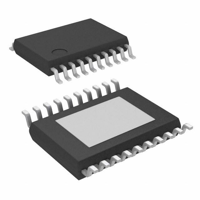
20-Pin PowerPAD™ TSSOP Package
Thermal Shutdown Protection
DESCRIPTION
The TPS70175 is designed to provide a complete
power management solution for the TMS320™ DSP
family, processor power, ASIC, FPGA, and digital
applications where dual output voltage regulators are
required. Easy programmability of the sequencing
function makes the TPS70175 ideal for any TMS320
DSP
applications
with
power
sequencing
requirements. Differentiated features, such as
accuracy, fast transient response, SVS supervisory
circuit, manual reset inputs, and an enable function,
provide a complete system solution.
The TPS70175 voltage regulator offers low dropout
voltage and dual outputs with power-up sequence
control, which is designed primarily for DSP
applications. These devices have extremely low noise
output performance without using any added filter
bypass capacitors and are designed to have a fast
transient response and be stable with 10-mF low ESR
capacitors.
This device has a fixed 5 V/2.5 V voltage option.
Regulator 1 can support up to 500 mA and regulator
2 can support up to 250 mA. Separate voltage inputs
allow the designer to configure the source power.
PWP PACKAGE
(TOP VIEW)
NC
VIN1
VIN1
MR1
MR2
EN
SEQ
GND
VIN2
VIN2
1
2
3
4
5
6
7
8
9
10
20
19
18
17
16
15
14
13
12
11
NC
VOUT1
VOUT1
VSENSE1/FB1
PG1
RESET
VSENSE2/FB2
VOUT2
VOUT2
NC
1
2
Please be aware that an important notice concerning availability, standard warranty, and use in critical applications of Texas
Instruments semiconductor products and disclaimers thereto appears at the end of this data sheet.
PowerPAD, TMS320 are trademarks of Texas Instruments.
PRODUCTION DATA information is current as of publication date.
Products conform to specifications per the terms of the Texas
Instruments standard warranty. Production processing does not
necessarily include testing of all parameters.
Copyright © 2005–2010, Texas Instruments Incorporated
�TPS70175-Q1
SGLS300B – MARCH 2005 – REVISED SEPTEMBER 2010
www.ti.com
TPS70175 PWP
6V
VIN1
0.1 µF
250 kΩ
PG1
PG1
MR2
MR2
>2 V
2 V
EN
250 kΩ
RESET
RESET
EN
MR1
I/O
10 µF
VSENSE1
VIN2
DSP
5V
VOUT1
MR1
>2 V
2 V
2 V
很抱歉,暂时无法提供与“TPS70175QPWPRQ1”相匹配的价格&库存,您可以联系我们找货
免费人工找货- 国内价格
- 1+72.25690
- 200+60.21410
- 500+48.17120
- 1000+40.14270