User's Guide
SLVU689A – June 2011 – Revised September 2012
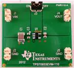
TPS709xxEVM-110 Evaluation Module
This User’s Guide describes the operational use of the TPS709xxEVM-110 Evaluation Module (EVM) as a
reference design for engineering demonstration and evaluation of the TPS709xx, low dropout linear
regulator (LDO). Included in this user’s guide are setup instructions, a schematic diagram, board layout,
thermal guidelines, a bill of materials, and test results.
1
2
3
4
5
6
Contents
Introduction ..................................................................................................................
Setup .........................................................................................................................
2.1
Input/Output Connectors and Jumper Descriptions ...........................................................
2.2
Equipment Setup ...................................................................................................
Operation .....................................................................................................................
Test Results .................................................................................................................
4.1
Turn-on Waveform .................................................................................................
4.2
Turn-off Waveform .................................................................................................
4.3
Load Transient Waveform ........................................................................................
4.4
PSRR ................................................................................................................
Thermal Guidelines and Layout Recommendations ...................................................................
Board Layout ................................................................................................................
2
2
2
2
2
3
3
4
4
5
6
6
List of Figures
..............................................
1
Turn-on Waveforms Into Full Load (22 Ω) of the TPS70933EVM-110
2
Turn-off Waveforms of the TPS70933EVM-110 ........................................................................ 4
3
Load Step and Transient Response of the TPS70933EVM-110
4
PSRR of the TPS70933EVM for Various Output Currents ............................................................ 5
5
PSRR of the TPS70933EVM for Various Input Voltages .............................................................. 5
6
TPS709xxEVM-110 Assembly Layer ..................................................................................... 6
7
TPS709xxEVM-110 Top Layer Routing .................................................................................. 6
8
TPS709xxEVM-110 Bottom Layer Routing .............................................................................. 7
9
TPS709xxEVM-110 Schematic
.....................................................
...........................................................................................
3
4
7
List of Tables
1
Thermal Resistance, θJA, and Maximum Power Dissipation........................................................... 6
2
TPS709xxEVM-110 Bill of Materials...................................................................................... 7
SLVU689A – June 2011 – Revised September 2012
Submit Documentation Feedback
TPS709xxEVM-110 Evaluation Module
Copyright © 2011–2012, Texas Instruments Incorporated
1
�Introduction
1
www.ti.com
Introduction
The TI TPS709xxEVM-110 Evaluation Module (EVM) helps design engineers evaluate the operation and
performance of the TPS709xx family of linear regulators for possible use in their own circuit application.
This EVM configuration contains a single linear regulator with internal thermal protection, reverse current
protection, and overcurrent protection in a SOT23-5 package. The regulator is capable of delivering up to
150 mA to the load, depending on the input-output power dissipation across the part which can be
minimized because of the low dropout voltage. The input and output capacitors for the TPS709xx must be
2.2 µF (effective minimum) for stability. An additional input capacitor connection is added to the EVM if
smaller, lower voltage capacitors are desired.
2
Setup
This section describes the jumpers and connectors on the EVM as well as how to properly connect, setup,
and use the TPS709xxEVM-110.
2.1
Input/Output Connectors and Jumper Descriptions
2.1.1
J1 – VIN
J1 is the input power supply voltage connector. The positive input lead and ground return lead from the
input power supply should be twisted and kept as short as possible to minimize EMI transmission.
Additional bulk capacitance should be added between J1 and J2 if the supply leads are greater than six
inches. For example, an additional 47-µF electrolytic capacitor connected from J1 to ground eliminates
unwanted ringing on the input due to long wires.
2.1.2
J2 – GND
J2 is the return connector for the input power supply.
2.1.3
J3 – EN
This jumper enables or disables the output of the TPS709xx. Placing a shorting jumper between pins 1
and 2 (OFF position) disables the TPS709xx. There is a pull-up resistor connected internally in the device;
therefore, removing the jumper enables the TPS709xx. The maximum rating of EN is 7 V. If EN is
connected to VIN or an external voltage source, be sure EN does not exceed 7 V.
2.1.4
J4 – VOUT
J4 is the regulated output voltage connector.
2.1.5
J5 – GND
J5, the return connector for VOUT, is connected to J2 on the PCB.
2.2
Equipment Setup
•
•
3
Operation
•
•
2
Set the power supply voltage to the desired operating input voltage. Turn the power supply off.
Connect the positive voltage lead from the power supply to J1 (VIN). Connect the ground lead from the
power supply to J2 (GND).
Connect a 0- to 150-mA load between J4 (VOUT) and J5 (GND).
Turn on the power supply.
Vary the respective load and input voltage as necessary, for test purposes.
TPS709xxEVM-110 Evaluation Module
SLVU689A – June 2011 – Revised September 2012
Submit Documentation Feedback
Copyright © 2011–2012, Texas Instruments Incorporated
�Test Results
www.ti.com
4
Test Results
This section provides typical performance waveforms for the EVM. Actual performance data is affected by
measurement techniques and environmental variables; therefore, these curves are presented for
reference and may differ from actual results obtained.
4.1
Turn-on Waveform
Figure 1 shows the turn-on characteristic, where 5 V is applied to VIN. The output drives a 22-Ω load (full
load).
Figure 1. Turn-on Waveforms Into Full Load (22 Ω) of the TPS70933EVM-110
SLVU689A – June 2011 – Revised September 2012
Submit Documentation Feedback
TPS709xxEVM-110 Evaluation Module
Copyright © 2011–2012, Texas Instruments Incorporated
3
�Test Results
4.2
www.ti.com
Turn-off Waveform
Figure 2 shows the turn-off characteristic, where 5 V is applied to VIN. The output drives a 22-Ω load.
Figure 2. Turn-off Waveforms of the TPS70933EVM-110
4.3
Load Transient Waveform
Figure 3 shows the load transient response for a load-step transient from 15 mA to 135 mA, where 5 V is
applied to VIN.
Figure 3. Load Step and Transient Response of the TPS70933EVM-110
4
TPS709xxEVM-110 Evaluation Module
SLVU689A – June 2011 – Revised September 2012
Submit Documentation Feedback
Copyright © 2011–2012, Texas Instruments Incorporated
�Test Results
www.ti.com
4.4
PSRR
Figure 4 shows the PSRR of the TPS70933EVM-110 at different load currents and Figure 5 shows the
PSRR of the TPS70933EVM-110 at different input voltages.
Figure 4. PSRR of the TPS70933EVM for Various Output Currents
100
VIN = 4.3 V
VIN = 5.0 V
VIN = 7.0 V
VIN = 10 V
90
80
PSRR (dB)
70
60
50
40
30
20
10
0
10
100
1k
10k
100k
Frequency (Hz)
1M
10M
G002
Figure 5. PSRR of the TPS70933EVM for Various Input Voltages
SLVU689A – June 2011 – Revised September 2012
Submit Documentation Feedback
TPS709xxEVM-110 Evaluation Module
Copyright © 2011–2012, Texas Instruments Incorporated
5
�Thermal Guidelines and Layout Recommendations
5
www.ti.com
Thermal Guidelines and Layout Recommendations
Thermal management is a key component in the design of any power converter and is especially
important when the power dissipation in the LDO is high. Use the following formula to approximate the
maximum power dissipation for the ambient temperature:
TJ = TA + PD × θJA
Where TJ is the junction temperature, TA is the ambient temperature, PD is the power dissipation in the
device (Watts), and θJA is the thermal resistance from junction to ambient. All temperatures are in degrees
Celsius. The maximum operating junction temperature, TJ, must not be allowed to exceed 125°C. The
layout design must be copper trace and plane areas smartly, as thermal sinks, in order to not allow TJ to
exceed the absolute maximum rating under all temperature and voltage conditions across the part.
Table 1 repeats information from the Dissipation Ratings Table of the TPS709xx-series datasheet for
comparison with the thermal resistance, θJA, for High-K JEDEC standard boards. The maximum input
voltage can be calculated for full loads at different ambient temperatures. The input voltage must be less
than these values in order to maintain a safe junction temperature.
Table 1. Thermal Resistance, θJA, and Maximum Power Dissipation
Package
θJA
Max VIN @ 150 mA (TA = 25°C)
Max VIN @ 150 mA (TA = 70°C)
DBV
212°C/W
6.4 V
5.0 V
Board Layout
J1
C3
C1
J2
J4
J3
U1
C2
6
Board
High-K
J5
Figure 6. TPS709xxEVM-110 Assembly Layer
Figure 7. TPS709xxEVM-110 Top Layer Routing
6
TPS709xxEVM-110 Evaluation Module
SLVU689A – June 2011 – Revised September 2012
Submit Documentation Feedback
Copyright © 2011–2012, Texas Instruments Incorporated
�Board Layout
www.ti.com
Figure 8. TPS709xxEVM-110 Bottom Layer Routing
Figure 9. TPS709xxEVM-110 Schematic
Table 2. TPS709xxEVM-110 Bill of Materials
Count
RefDes
Value
Description
Size
Part Number
MFR
1
C1
2.2 µF
Capacitor, ceramic chip, 50 V, X7R, ±10%
1210
STD
STD
1
C2
2.2 µF
Capacitor, ceramic chip, 6.3 V, X7R, ±10%
0603
STD
STD
0
C3
DNP
Capacitor, ceramic chip
0603
STD
STD
5
J1-5
PEC02SAAN
0.100 in × 2
PEC02SAAN
Sullins
1
U1
TPS70933DBV
IC, 150 mA, ultra-low IQ, 1-µA LDO regulator with enable
SOT-23
TPS709xxDBV
TI
1
J3
Shunt, black
100 mil
929950-00
3M
1
–
PWR110
Any
Notes:
–
Header, Male 2-pin, 100mil spacing
PCB, 1.20 in × 1.30 in × 0.062 in
1. These assemblies are ESD sensitive, observe ESD precautions.
2. These assemblies must be clean and free from flux and all contaminants. Use of no-clean flux is not acceptable.
3. These assemblies must comply with workmanship standards IPC-A-610 Class 2.
4. Ref designators marked with an asterisk ('**') cannot be substituted. All other components can be substituted with equivalent MFG's components.
spacer
SLVU689A – June 2011 – Revised September 2012
Submit Documentation Feedback
TPS709xxEVM-110 Evaluation Module
Copyright © 2011–2012, Texas Instruments Incorporated
7
�Evaluation Board/Kit Important Notice
Texas Instruments (TI) provides the enclosed product(s) under the following conditions:
This evaluation board/kit is intended for use for ENGINEERING DEVELOPMENT, DEMONSTRATION, OR EVALUATION PURPOSES
ONLY and is not considered by TI to be a finished end-product fit for general consumer use. Persons handling the product(s) must have
electronics training and observe good engineering practice standards. As such, the goods being provided are not intended to be complete
in terms of required design-, marketing-, and/or manufacturing-related protective considerations, including product safety and environmental
measures typically found in end products that incorporate such semiconductor components or circuit boards. This evaluation board/kit does
not fall within the scope of the European Union directives regarding electromagnetic compatibility, restricted substances (RoHS), recycling
(WEEE), FCC, CE or UL, and therefore may not meet the technical requirements of these directives or other related directives.
Should this evaluation board/kit not meet the specifications indicated in the User’s Guide, the board/kit may be returned within 30 days from
the date of delivery for a full refund. THE FOREGOING WARRANTY IS THE EXCLUSIVE WARRANTY MADE BY SELLER TO BUYER
AND IS IN LIEU OF ALL OTHER WARRANTIES, EXPRESSED, IMPLIED, OR STATUTORY, INCLUDING ANY WARRANTY OF
MERCHANTABILITY OR FITNESS FOR ANY PARTICULAR PURPOSE.
The user assumes all responsibility and liability for proper and safe handling of the goods. Further, the user indemnifies TI from all claims
arising from the handling or use of the goods. Due to the open construction of the product, it is the user’s responsibility to take any and all
appropriate precautions with regard to electrostatic discharge.
EXCEPT TO THE EXTENT OF THE INDEMNITY SET FORTH ABOVE, NEITHER PARTY SHALL BE LIABLE TO THE OTHER FOR ANY
INDIRECT, SPECIAL, INCIDENTAL, OR CONSEQUENTIAL DAMAGES.
TI currently deals with a variety of customers for products, and therefore our arrangement with the user is not exclusive.
TI assumes no liability for applications assistance, customer product design, software performance, or infringement of patents or
services described herein.
Please read the User’s Guide and, specifically, the Warnings and Restrictions notice in the User’s Guide prior to handling the product. This
notice contains important safety information about temperatures and voltages. For additional information on TI’s environmental and/or
safety programs, please contact the TI application engineer or visit www.ti.com/esh.
No license is granted under any patent right or other intellectual property right of TI covering or relating to any machine, process, or
combination in which such TI products or services might be or are used.
FCC Warning
This evaluation board/kit is intended for use for ENGINEERING DEVELOPMENT, DEMONSTRATION, OR EVALUATION PURPOSES
ONLY and is not considered by TI to be a finished end-product fit for general consumer use. It generates, uses, and can radiate radio
frequency energy and has not been tested for compliance with the limits of computing devices pursuant to part 15 of FCC rules, which are
designed to provide reasonable protection against radio frequency interference. Operation of this equipment in other environments may
cause interference with radio communications, in which case the user at his own expense will be required to take whatever measures may
be required to correct this interference.
EVM Warnings and Restrictions
It is important to operate this EVM within the input voltage range of -22 V to 0.3 V and the output voltage range of -20 V to -3 V .
Exceeding the specified input range may cause unexpected operation and/or irreversible damage to the EVM. If there are questions
concerning the input range, please contact a TI field representative prior to connecting the input power.
Applying loads outside of the specified output range may result in unintended operation and/or possible permanent damage to the EVM.
Please consult the EVM User's Guide prior to connecting any load to the EVM output. If there is uncertainty as to the load specification,
please contact a TI field representative.
During normal operation, some circuit components may have case temperatures greater than 125° C. The EVM is designed to operate
properly with certain components above 125° C as long as the input and output ranges are maintained. These components include but are
not limited to linear regulators, switching transistors, pass transistors, and current sense resistors. These types of devices can be identified
using the EVM schematic located in the EVM User's Guide. When placing measurement probes near these devices during operation,
please be aware that these devices may be very warm to the touch.
Mailing Address: Texas Instruments, Post Office Box 655303, Dallas, Texas 75265
Copyright © 2012, Texas Instruments Incorporated
�IMPORTANT NOTICE
Texas Instruments Incorporated and its subsidiaries (TI) reserve the right to make corrections, enhancements, improvements and other
changes to its semiconductor products and services per JESD46, latest issue, and to discontinue any product or service per JESD48, latest
issue. Buyers should obtain the latest relevant information before placing orders and should verify that such information is current and
complete. All semiconductor products (also referred to herein as “components”) are sold subject to TI’s terms and conditions of sale
supplied at the time of order acknowledgment.
TI warrants performance of its components to the specifications applicable at the time of sale, in accordance with the warranty in TI’s terms
and conditions of sale of semiconductor products. Testing and other quality control techniques are used to the extent TI deems necessary
to support this warranty. Except where mandated by applicable law, testing of all parameters of each component is not necessarily
performed.
TI assumes no liability for applications assistance or the design of Buyers’ products. Buyers are responsible for their products and
applications using TI components. To minimize the risks associated with Buyers’ products and applications, Buyers should provide
adequate design and operating safeguards.
TI does not warrant or represent that any license, either express or implied, is granted under any patent right, copyright, mask work right, or
other intellectual property right relating to any combination, machine, or process in which TI components or services are used. Information
published by TI regarding third-party products or services does not constitute a license to use such products or services or a warranty or
endorsement thereof. Use of such information may require a license from a third party under the patents or other intellectual property of the
third party, or a license from TI under the patents or other intellectual property of TI.
Reproduction of significant portions of TI information in TI data books or data sheets is permissible only if reproduction is without alteration
and is accompanied by all associated warranties, conditions, limitations, and notices. TI is not responsible or liable for such altered
documentation. Information of third parties may be subject to additional restrictions.
Resale of TI components or services with statements different from or beyond the parameters stated by TI for that component or service
voids all express and any implied warranties for the associated TI component or service and is an unfair and deceptive business practice.
TI is not responsible or liable for any such statements.
Buyer acknowledges and agrees that it is solely responsible for compliance with all legal, regulatory and safety-related requirements
concerning its products, and any use of TI components in its applications, notwithstanding any applications-related information or support
that may be provided by TI. Buyer represents and agrees that it has all the necessary expertise to create and implement safeguards which
anticipate dangerous consequences of failures, monitor failures and their consequences, lessen the likelihood of failures that might cause
harm and take appropriate remedial actions. Buyer will fully indemnify TI and its representatives against any damages arising out of the use
of any TI components in safety-critical applications.
In some cases, TI components may be promoted specifically to facilitate safety-related applications. With such components, TI’s goal is to
help enable customers to design and create their own end-product solutions that meet applicable functional safety standards and
requirements. Nonetheless, such components are subject to these terms.
No TI components are authorized for use in FDA Class III (or similar life-critical medical equipment) unless authorized officers of the parties
have executed a special agreement specifically governing such use.
Only those TI components which TI has specifically designated as military grade or “enhanced plastic” are designed and intended for use in
military/aerospace applications or environments. Buyer acknowledges and agrees that any military or aerospace use of TI components
which have not been so designated is solely at the Buyer's risk, and that Buyer is solely responsible for compliance with all legal and
regulatory requirements in connection with such use.
TI has specifically designated certain components which meet ISO/TS16949 requirements, mainly for automotive use. Components which
have not been so designated are neither designed nor intended for automotive use; and TI will not be responsible for any failure of such
components to meet such requirements.
Products
Applications
Audio
www.ti.com/audio
Automotive and Transportation
www.ti.com/automotive
Amplifiers
amplifier.ti.com
Communications and Telecom
www.ti.com/communications
Data Converters
dataconverter.ti.com
Computers and Peripherals
www.ti.com/computers
DLP® Products
www.dlp.com
Consumer Electronics
www.ti.com/consumer-apps
DSP
dsp.ti.com
Energy and Lighting
www.ti.com/energy
Clocks and Timers
www.ti.com/clocks
Industrial
www.ti.com/industrial
Interface
interface.ti.com
Medical
www.ti.com/medical
Logic
logic.ti.com
Security
www.ti.com/security
Power Mgmt
power.ti.com
Space, Avionics and Defense
www.ti.com/space-avionics-defense
Microcontrollers
microcontroller.ti.com
Video and Imaging
www.ti.com/video
RFID
www.ti-rfid.com
OMAP Applications Processors
www.ti.com/omap
TI E2E Community
e2e.ti.com
Wireless Connectivity
www.ti.com/wirelessconnectivity
Mailing Address: Texas Instruments, Post Office Box 655303, Dallas, Texas 75265
Copyright © 2012, Texas Instruments Incorporated
�