TPS71202-EP
��
��� �
�
�� �� � � ���
www.ti.com
SGLS395A – OCTOBER 2008 – REVISED SEPTEMBER 2010
DUAL, 250-mA OUTPUT, ULTRA-LOW NOISE, HIGH PSRR, LOW-DROPOUT
LINEAR REGULATOR
Check for Samples: TPS71202-EP
FEATURES
1
•
•
•
•
•
•
•
•
•
•
•
Dual 250-mA High-Performance RF LDOs
Adjustable Output Voltage (1.2 V to 5.5 V)
High PSRR: 65 dB at 10 kHz
Ultra-Low Noise: 32 mVrms
Fast Start-Up Time: 60 ms
Stable with 2.2-mF Ceramic Capacitor
Excellent Load/Line Transient Response
Very Low Dropout Voltage: 125 mV at 250 mA
Independent Enable Pins
Thermal Shutdown and Independent Current
Limit
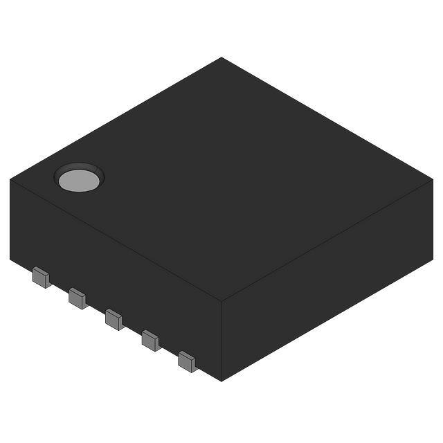
Available in Thermally-Enhanced SON
Package: 3 mm × 3 mm × 1 mm
APPLICATIONS
•
•
•
•
•
Cellular and Cordless Phones
Wireless PDA/Handheld Products
PCMCIA/Wireless LAN Applications
Digital Camera/Camcorder/Internet Audio
DSP/FPGA/ASIC/Controllers and Processors
SUPPORTS DEFENSE, AEROSPACE,
AND MEDICAL APPLICATIONS
•
•
•
•
•
•
•
Controlled Baseline
One Assembly/Test Site
One Fabrication Site
Available in Military (–55°C/125°C)
Temperature Range (1)
Extended Product Life Cycle
Extended Product-Change Notification
Product Traceability
DESCRIPTION
The TPS71202 low-dropout (LDO) voltage regulator
is tailored to noise-sensitive and RF applications. It
features dual 250-mA LDOs with ultra-low noise, high
power-supply rejection ratio (PSRR), and fast
transient and start-up response. Each regulator
output is stable with low-cost 2.2-mF ceramic output
capacitors and features very low dropout voltages
(125 mV typical at 250 mA). The regulator achieves
fast start-up times (approximately 60 ms with a
0.001-mF bypass capacitor) while consuming very low
quiescent current (300 mA typical with both outputs
enabled). When the device is placed in standby
mode, the supply current is reduced to less than
0.3 mA typical. The regulator exhibits approximately
32 mVrms of output voltage noise with VOUT = 2.8 V
and a 0.01-mF noise reduction (NR) capacitor.
Applications with analog components that are
noise-sensitive, such as portable RF electronics,
benefit from high PSRR, low noise, and fast line and
load transient features. The TPS71202 is offered in a
thin 3-mm × 3-mm SON package and is fully
specified from –55°C to 125°C (TJ).
(1)
Custom temperature ranges available
1
Please be aware that an important notice concerning availability, standard warranty, and use in critical applications of Texas
Instruments semiconductor products and disclaimers thereto appears at the end of this data sheet.
PRODUCTION DATA information is current as of publication date.
Products conform to specifications per the terms of the Texas
Instruments standard warranty. Production processing does not
necessarily include testing of all parameters.
Copyright © 2008–2010, Texas Instruments Incorporated
On products compliant to MIL-PRF-38535, all parameters are
tested unless otherwise noted. On all other products, production
processing does not necessarily include testing of all parameters.
�TPS71202-EP
SGLS395A – OCTOBER 2008 – REVISED SEPTEMBER 2010
www.ti.com
This integrated circuit can be damaged by ESD. Texas Instruments recommends that all integrated circuits be handled with
appropriate precautions. Failure to observe proper handling and installation procedures can cause damage.
ESD damage can range from subtle performance degradation to complete device failure. Precision integrated circuits may be more
susceptible to damage because very small parametric changes could cause the device not to meet its published specifications.
PSRR (RIPPLE REJECTION) vs FREQUENCY
80
70
DRC PACKAGE
3-mm y 3-mm SON
(TOP VIEW)
10 EN1
9 FB1
OUT1 3
8 EN2
7 FB2
OUT2 4
GND 5
PSRR (dB)
IN 1
NC 2
IOUT = 250 mA
60
50
40
IOUT = 1 mA
30
20
6 NR
VOUT = 2.8 V
COUT = 2.2 µF
CNR = 0.01 µF
10
0
10
100
1k
10k
100k
1M
10M
Frequency (Hz)
ORDERING INFORMATION (1)
PACKAGE (2)
TJ
–55°C to 125°C
(1)
(2)
SON-10 – DRC
ORDERABLE PART NUMBER
Reel of 250
TPS71202MDRCTEP
TOP-SIDE MARKING
CVQ
For the most current package and ordering information, see the Package Option Addendum at the end of this document, or see the TI
web site at www.ti.com.
Package drawings, thermal data, and symbolization are available at www.ti.com/packaging.
ABSOLUTE MAXIMUM RATINGS
over operating junction temperature range unless otherwise noted (1)
VIN
Input voltage range
IN
VEN1,
VEN2
Input voltage range
EN1, EN2
VOUT
Output voltage range
OUT
–0.3 V to 6 V
–0.3 V to VIN + 0.3 V
–0.3 V to 6 V
Peak output current
Internally limited
Output short-circuit duration
Indefinite
Continuous total power dissipation
TJ
See Thermal Information table
Junction temperature range
–55°C to 150°C
Storage temperature range
ESD
(1)
2
Electrostatic discharge rating
–65°C to 150°C
Human-Body Model (HBM)
2000 V
Charged-Device Model (CDM)
500 V
Stresses beyond those listed under absolute maximum ratings may cause permanent damage to the device. These are stress ratings
only, and functional operation of the device at these or any other conditions beyond those indicated under the Electrical Characteristics
is not implied. Exposure to absolute maximum rated conditions for extended periods may affect device reliability.
Submit Documentation Feedback
Copyright © 2008–2010, Texas Instruments Incorporated
Product Folder Link(s): TPS71202-EP
�TPS71202-EP
www.ti.com
SGLS395A – OCTOBER 2008 – REVISED SEPTEMBER 2010
THERMAL INFORMATION
TPS71202-EP
THERMAL METRIC (1) (2)
DRC (10 PINS)
qJA
Junction-to-ambient thermal resistance
49.6
qJCtop
Junction-to-case (top) thermal resistance
70.0
qJB
Junction-to-board thermal resistance
17.8
yJT
Junction-to-top characterization parameter
0.6
yJB
Junction-to-board characterization parameter
15.2
qJCbot
Junction-to-case (bottom) thermal resistance
5.2
(1)
(2)
UNITS
°C/W
For more information about traditional and new thermal metrics, see the IC Package Thermal Metrics application report, SPRA953.
For thermal estimates of this device based on PCB copper area, see the TI PCB Thermal Calculator.
ELECTRICAL CHARACTERISTICS
over operating temperature range (TJ = –55°C to +125°C), VIN = highest (VOUT(nom) + 1 V) or 2.7 V (whichever is greater),
IOUT = 1 mA, VEN1, 2 = 1.2 V, COUT = 10 mF, CNR = 0.01 mF, and adjustable LDOs are tested at VOUT = 3.0 V (unless otherwise
noted). Typical values are at TJ = 25°C.
PARAMETER
TEST CONDITIONS
VIN
Input voltage range (1)
VFB
Internal reference (adjustable LDOs)
MIN
Accuracy (1)
Nominal
TJ = +25°C, IOUT = 0 mA
Over VIN,
IOUT, and
temperatur
e
VOUT + 1.0 V ≤ VIN ≤ 5.5 V,
0 mA ≤ IOUT ≤ 250 mA
ΔVOUT%/ΔVIN
Line regulation (1)
VOUT + 1.0 V ≤ VIN ≤ 5.5 V
ΔVOUT%/ΔIOU
Load regulation
VDO
Dropout voltage
(VIN = VOUT(nom) – 0.1V)
ICL
Output current limit
T
IGND
Ground pin current
ISHDN
Shutdown current (2)
IFB
FB pin current
1.250
V
VFB
5.5 – VDO
V
–1.5
+1.5
–3
1.225
1
+3
%
0.05
%/V
0 mA ≤ IOUT ≤ 250 mA
0.8
%/mA
IOUT1 = IOUT2 = 250 mA
125
315
mV
600
800
mA
VOUT = 0.9 × VOUT(nom)
400
One LDO
enabled
IOUT = 1 mA (enabled channel)
190
250
Both LDOs
enabled
IOUT1 = IOUT2 = 1 mA to 250 mA
300
600
VEN ≤ 0.4 V, 0 V ≤ VIN ≤ 5.5 V
0.3
2.0
mA
0.1
1.50
mA
mA
Vn
Output noise voltage,
BW = 10 Hz to 100 kHz
PSRR
Power-supply rejection ratio
(ripple rejection)
f = 100 Hz, IOUT = 250 mA
65
f = 10 kHz, IOUT = 250 mA
65
tSTR
Startup time
VOUT = 2.85 V, RL = 30Ω, CNR = 0.001 mF
60
VIH
Enable threshold high (EN1, EN2)
VIL
Enable threshold low (EN1, EN2)
IEN
Enable pin current (EN1, EN2)
TSD
Thermal shutdown temperature
(1)
(2)
UNIT
V
No CNR, IOUT = 250 mA
UVLO
MAX
5.5
1.200
Output voltage range
(adjustable LDOs)
VOUT
TYP
2.7
80.0 × VOUT
CNR = 0.01 mF, IOUT = 250 mA
11.8 × VOUT
VIN = VEN = 5.5 V
VIN
0.4
V
–1
1
mA
Temp increasing
+160
Temp decreasing
+140
VIN rising
VIN falling
ms
0
Reset
Undervoltage lockout hysteresis
dB
1.2
Shutdown
Undervoltage lockout threshold
mVrms
2.25
V
°C
2.65
100
V
mV
Minimum VIN = (VOUT + VDO) or 2.7 V, whichever is greater.
For the adjustable version, this applies only after VIN is applied; then VEN transitions from high to low.
Submit Documentation Feedback
Copyright © 2008–2010, Texas Instruments Incorporated
Product Folder Link(s): TPS71202-EP
3
�TPS71202-EP
SGLS395A – OCTOBER 2008 – REVISED SEPTEMBER 2010
www.ti.com
FUNCTIONAL BLOCK DIAGRAM —
FIXED VERSION
IN
FUNCTIONAL BLOCK DIAGRAM —
ADJUSTABLE VERSION
OUT1
IN
OUT1
30 µA
Current
Limit
Current
Limit
90 kΩ
FB1
EN1
EN1
Thermal
Shutdown
Thermal
Shutdown
OUT2
UVLO
OUT2
30 µA
Current
Limit
Current
Limit
UVLO
90 kΩ
FB2
EN2
EN2
250 kΩ
250 kΩ
NR
VREF
5 pF
1.225 V
TPS712xx
Fixed/Fixed
Quickstart
NR
VREF
5 pF
1.225 V
Quickstart
TPS712xx
Adj/Adj
Table 1. TERMINAL FUNCTIONS
TERMINAL
NAME
4
DESCRIPTION
DRC
IN
1
GND
5, Pad
Unregulated input supply. A small 0.1-mF capacitor should be connected from IN to GND.
OUT1
3
Output of the regulator. A small 2.2-mF ceramic capacitor is required from this pin to ground to assure
stability.
OUT2
4
Same as OUT1 but for LDO2.
EN1
10
Driving the enable pin (EN) high turns on LDO1. Driving this pin low puts LDO1 into shutdown mode,
reducing operating current. The enable pin should be connected to IN if not used.
EN2
8
Same as EN1 but controls LDO2.
FB1
9
Feedback for channel 1
FB2
7
Feedback for channel 2
NR
6
Noise reduction pin; connect an external bypass capacitor to reduce LDO output noise.
NC
2
No connection.
Ground
Submit Documentation Feedback
Copyright © 2008–2010, Texas Instruments Incorporated
Product Folder Link(s): TPS71202-EP
�TPS71202-EP
www.ti.com
SGLS395A – OCTOBER 2008 – REVISED SEPTEMBER 2010
TYPICAL CHARACTERISTICS
For all voltage versions at TJ = 25°C, VIN = VOUT(nom) + 1 V, IOUT = 1 mA,VEN = 1.2 V, COUT = 2.2 mF, and CNR = 0.01 mF
(unless otherwise noted)
OUTPUT VOLTAGE vs INPUT VOLTAGE
OUTPUT VOLTAGE vs OUTPUT CURRENT
1.0
1.0
0.8
0.8
0.6
0.6
0.4
+25_ C
0.2
VOUT (%)
VOUT (%)
0.4
0
−0.2
+125_ C
−0.4
−0.6
0
−40_C
−0.2
−0.4
−0.6
−40_C
−0.8
+25_C
0.2
−0.8
−1.0
+125_ C
−1.0
3.0
3.5
4.0
4.5
5.0
5.5
6.0
0
50
100
VIN (V)
150
200
250
IOUT (mA)
Figure 1.
Figure 2.
OUTPUT VOLTAGE vs TEMPERATURE
DROPOUT VOLTAGE vs INPUT VOLTAGE
(ADJUSTABLE VERSION)
200
1.0
180
160
VOUT (%)
IOUT = 10 mA
0
IOUT = 125 mA
−0.5
IOUT = 250 mA
−1.0
Dropout Voltage (mV)
0.5
TJ = +125_C
140
120
TJ = +25_C
100
80
60
TJ = −40_C
40
20
−1.5
−40 −25 −10
0
5
20
35
50
65
80
95
2.7
110 125
2.9
3.1
3.3
3.5
3.7
3.9 4.1
4.3
4.5 4.7
4.9
VIN (V)
Junction Temperature (_C)
Figure 3.
Figure 4.
TPS71256
DROPOUT VOLTAGE vs OUTPUT CURRENT
TPS71256
DROPOUT VOLTAGE vs JUNCTION TEMPERATURE
200
250
200
150
Dropout Voltage (mV)
Dropout Voltage (mV)
TJ = +125_C
100
TJ = −40_ C
TJ = +25_C
50
150
IOUT = 250 mA
100
50
0
0
50
100
150
200
250
0
−40 −25 −10
IOUT (mA)
5
20
35
50
65
80
95
110 125
Junction Temperature (°C)
Figure 5.
Figure 6.
Submit Documentation Feedback
Copyright © 2008–2010, Texas Instruments Incorporated
Product Folder Link(s): TPS71202-EP
5
�TPS71202-EP
SGLS395A – OCTOBER 2008 – REVISED SEPTEMBER 2010
www.ti.com
TYPICAL CHARACTERISTICS (continued)
For all voltage versions at TJ = 25°C, VIN = VOUT(nom) + 1 V, IOUT = 1 mA,VEN = 1.2 V, COUT = 2.2 mF, and CNR = 0.01 mF
(unless otherwise noted)
GROUND PIN CURRENT vs INPUT VOLTAGE
GROUND PIN CURRENT vs IOUT
400
400
375
375
350
+125_ C
325
IGND (µA)
IGND (µA)
350
300
275
−40_C
+25_C
250
325
+125_C
300
275
225
+25_ C
−40_C
250
225
200
200
2.7
3.2
3.7
4.2
4.7
5.2
5.7
0
50
100
VIN (V)
200
250
Figure 7.
Figure 8.
GROUND PIN CURRENT vs JUNCTION TEMPERATURE
GROUND PIN CURRENT vs JUNCTION TEMPERATURE
(DISABLED)
500
400
VEN1 = VEN2 = 1.2V
375
VEN1 = VEN2 = 0.4V
450
VIN = 3.8 V
VIN = 3.8 V
400
350
350
325
IGND (nA)
IGND (µA)
150
IOUT (mA)
300
275
300
250
200
150
250
100
225
50
200
0
−40 −25 −10
5
20
35
50
65
80
95
110 125
−40 −25 −10
20
35
50
65
80
95
Figure 9.
Figure 10.
CURRENT LIMIT vs JUNCTION TEMPERATURE
TPS71256
LINE TRANSIENT RESPONSE
800
110 125
COUT1 = COUT2 = 10µF
VIN = 3.8 V
750
Current Limit (mA)
5
Junction Temperature (_C)
Junction Temperature (_C)
3.8 V
VIN
700
3.2 V
650
600
I OUT = 250 mA
10 mV/div
550
500
IOUT = 1 mA
10 mV/div
450
400
−40 −25 −10
5
20
35
50
65
80
95
110 125
VOUT1
VOUT2
100 µs/div
Junction Temperature (_C)
Figure 11.
6
Figure 12.
Submit Documentation Feedback
Copyright © 2008–2010, Texas Instruments Incorporated
Product Folder Link(s): TPS71202-EP
�TPS71202-EP
www.ti.com
SGLS395A – OCTOBER 2008 – REVISED SEPTEMBER 2010
TYPICAL CHARACTERISTICS (continued)
For all voltage versions at TJ = 25°C, VIN = VOUT(nom) + 1 V, IOUT = 1 mA,VEN = 1.2 V, COUT = 2.2 mF, and CNR = 0.01 mF
(unless otherwise noted)
TPS71256
LOAD TRANSIENT RESPONSE
AND VOUT2 CROSSTALK
TPS71256
CHANNEL-TO-CHANNEL ISOLATION vs FREQUENCY
60
COUT2 = 10 µF
VOUT2
COUT1 = 10 µF
100 mV/div
VOUT1
250 mA
10 mA
200 mA/div
50
Channel Isolation (dB)
2 mV/div
IOUT1
40
30
20
10
COUT1 = C OUT2 = 10 µF
IOUT1 = 0 mA to 500 mA Sinusoidal Load
IOUT2 = 25 mA
0
20 µs/div
0.1
1
10
100
1k
Frequency (Hz)
Figure 13.
Figure 14.
TPS71256
TURN-ON/TURN-OFF RESPONSE
AND VOUT2 CROSSTALK
TPS71229
POWER-UP/POWER-DOWN
CNR = 0.01 µF
I OUT1 = IOUT2 = 250 mA
COUT1 = COUT 2 = 10 µF
IOUT1 = I OUT2 = 250 mA
20 mV/div
VOUT2
VIN
1 V/div
CNR = 0.001 µF
VOUT1
VOUT2
VOUT1
1 V/div
VEN1
50 µs/div
TOTAL NOISE vs CNR
NOISE SPECTRAL DENSITY
COUT = 2.2 mF
COUT = 2.2 µF
IOUT = 250 mA
200
Total Noise (µVrms)
Figure 16.
COUT = 10 µF
IOUT = 250 mA
150
100
VOUT = 2.8 V
COUT = 2.2 µF
IOUT = 0 mA
COUT = 10 µF
IOUT = 0 mA
50
0
1
10
100
1k
10k
100k
350
Spectral Noise Density (nV/√Hz)
250
50 ms/div
Figure 15.
300
CNR = 0.1 µF
VOUT = 2.8 V
IOUT = 250 mA
250
200
IOUT = 1 mA
150
100
50
0
100
CNR (pF)
1k
10k
100k
Frequency (Hz)
Figure 17.
Figure 18.
Submit Documentation Feedback
Copyright © 2008–2010, Texas Instruments Incorporated
Product Folder Link(s): TPS71202-EP
7
�TPS71202-EP
SGLS395A – OCTOBER 2008 – REVISED SEPTEMBER 2010
www.ti.com
TYPICAL CHARACTERISTICS (continued)
For all voltage versions at TJ = 25°C, VIN = VOUT(nom) + 1 V, IOUT = 1 mA,VEN = 1.2 V, COUT = 2.2 mF, and CNR = 0.01 mF
(unless otherwise noted)
NOISE SPECTRAL DENSITY
COUT = 10 mF
NOISE SPECTRAL DENSITY vs CNR
2.0
CNR = 0.1 µF
VOUT = 2.8 V
300
Spectral Noise Density (µV/√Hz)
Spectral Noise Density (nV/√Hz)
350
250
200
IOUT = 10 mA
150
IOUT = 250 mA
100
50
0
100
1k
10k
COUT = 10 µF
IOUT = 250 mA
VOUT = 2.8 V
1.75
1.5
1.25
0.01 µF
0.75
0.5
0.1 µF
0.25
0
100
100k
Figure 19.
Figure 20.
70
IOUT = 250 mA
60
60
50
50
PSRR (dB)
PSRR (dB)
70
40
0
I OUT = 1 mA
100
IOUT = 1 mA
40
30
I OUT = 250 mA
20
VOUT = 2.8 V
COUT = 2.2 µF
CNR = 0.01 µF
10
VOUT = 2.8 V
COUT = 10 µF
CNR = 0.01 µF
10
0
1k
10k
100k
1M
100k
PSRR (RIPPLE REJECTION) vs FREQUENCY
80
10
10k
Frequency (Hz)
PSRR (RIPPLE REJECTION) vs FREQUENCY
20
1k
Frequency (Hz)
80
30
0.001 µF
0.047 µF
1.0
10M
10
100
1k
10k
100k
Frequency (Hz)
Frequency (Hz)
Figure 21.
Figure 22.
1M
10M
PSRR (RIPPLE REJECTION) vs VIN – VOUT
80
70
f = 1 kHz
PSRR (dB)
60
50
f = 10 kHz
40
30
f = 100 kHz
VOUT = 2.8 V
IOUT = 250 mA
COUT = 10 µF
CNR = 0.01 µF
20
10
0
0
0.2
0.4
0.6
0.8
1.0
1.2
1.4
1.6
1.8
2.0
VIN − VOUT (V)
Figure 23.
8
Submit Documentation Feedback
Copyright © 2008–2010, Texas Instruments Incorporated
Product Folder Link(s): TPS71202-EP
�TPS71202-EP
www.ti.com
SGLS395A – OCTOBER 2008 – REVISED SEPTEMBER 2010
APPLICATION INFORMATION
The TPS71202 dual low-dropout (LDO) regulator has
been optimized for use in noise-sensitive
battery-operated equipment. The device features
extremely low dropout, high PSRR, ultra-low output
noise, and low quiescent current (190 mA typical per
channel). When both outputs are disabled, the supply
currents are reduced to less than 2 mA.
INPUT AND OUTPUT CAPACITOR
REQUIREMENTS
A 0.1-mF or larger ceramic input bypass capacitor,
connected between IN and GND and located close to
the TPS71202, is required for stability. It improves
transient response, noise rejection, and ripple
rejection. A higher-value input capacitor may be
necessary if large, fast rise-time load transients are
anticipated and the device is located several inches
from the power source.
The TPS71202 requires an output capacitor
connected between the outputs and GND to stabilize
the
internal
control
loops.
The
minimum
recommended output capacitor is 2.2 mF. If an output
voltage of 1.8 V or less is chosen, the minimum
recommended output capacitor is 4.7 mF. Any
ceramic capacitor that meets the minimum output
capacitor requirements is suitable. Capacitors with
higher ESR may be used, provided the ESR is less
than 1 Ω.
OUTPUT NOISE
The internal voltage reference is a key source of
noise in an LDO regulator. The TPS71202 has an NR
pin that is connected to the voltage reference through
a 250-kΩ internal resistor. The 250-kΩ internal
resistor, in conjunction with an external ceramic
bypass capacitor connected to the NR pin, creates a
low-pass filter to reduce the voltage reference noise
and, therefore, the noise at the regulator output. To
achieve a fast startup, the 250-kΩ internal resistor is
shorted for 400 ms after the device is enabled.
Because the primary noise source is the internal
voltage reference, the output noise is greater for
higher output voltage versions. For the case where
no noise reduction capacitor is used, the typical noise
(mVrms) over 10 Hz to 100 kHz is 80 times the output
voltage. If a 0.01-mF capacitor is used from the NR
pin to ground, the noise (mVrms) drops to 11.8 times
the output voltage.
STARTUP CHARACTERISITCS
To minimize startup overshoot, the TPS71202 initially
targets an output voltage that is approximately 80%
of the final value. To avoid a delayed startup time,
noise reduction capacitors of 0.01 mF or less are
recommended. Larger noise reduction capacitors
cause the output to hold at 80% until the voltage on
the noise reduction capacitor exceeds 80% of the
bandgap voltage. The typical startup time with a
0.001-mF noise reduction capacitor is 60 ms. Once
one of the output voltages is present, the startup time
of the other output is not affected by the noise
reduction capacitor.
Submit Documentation Feedback
Copyright © 2008–2010, Texas Instruments Incorporated
Product Folder Link(s): TPS71202-EP
9
�TPS71202-EP
SGLS395A – OCTOBER 2008 – REVISED SEPTEMBER 2010
www.ti.com
PROGRAMMING THE TPS71202
ADJUSTABLE LDO REGULATOR
The output voltage of the TPS71202 dual adjustable
regulator is programmed using an external resistor
divider, as shown in Figure 24. The output voltage is
calculated using Equation 1:
V OUT + VREF
Ǔ
ǒ1 ) R1
R2
blank
(1)
where VREF = 1.225 V (the internal reference
voltage).
Resistors R2 and R4 should be chosen for
approximately a 40-mA divider current. Lower value
resistors can be used for improved noise
performance but consume more power. Higher values
should be avoided because leakage current at FB
increases the output voltage error. The recommended
design procedure is to choose R2 = 30.1 kΩ to set
the divider current at 40 mA, and then calculate R1
using Equation 2:
R1 +
ǒVV
OUT
REF
Ǔ
*1
For voltages ≤ 1.8 V, the value of this capacitor
should be 100 pF. For voltages > 1.8 V, the
approximate value of this capacitor can be calculated
as Equation 3:
(3 105) (R1 ) R2)
(pF)
C1 +
(R1 R2)
(3)
R2
(2)
To improve the stability and noise performance of the
adjustable version, a small compensation capacitor
can be placed between OUT and FB.
The suggested value of this capacitor for several
resistor ratios is shown in Figure 24. If this capacitor
is not used (such as in a unity-gain configuration) or if
an output voltage ≤ 1.8 V is chosen, then the
minimum recommended output capacitor is 4.7 mF
instead of 2.2 mF.
DROPOUT VOLTAGE
The TPS712xx uses a PMOS pass transistor to
achieve extremely low dropout. When (VIN - VOUT) is
less than the dropout voltage (VDO), the PMOS pass
device is in its linear region of operation and the
input-to-output resistance is the RDS, ON of the PMOS
pass element. Dropout voltages at lower currents can
be approximated by calculating the effective RDS, ON
of the pass element and multiplying that resistance by
the load current. RDS, ON of the pass element can be
obtained by dividing the dropout voltage by the rated
output current.
TPS71202
VIN
IN
VOUT1
OUT1
R1
EN1
C1
VOUT
FB1
R2
0.1 µF
EN2
VOUT2
OUT2
R3
NR
GND FB2
0.01 µF
Output Voltage Programming Guide
2.2 µF
R4
C2
2.2 µF
R1/R3
R2/R4
C1/C2
1.225 V
Short
Open
Open
1.5 V
7.15 kΩ
30.1 kΩ
100 pF
2.5 V
31.6 kΩ
30.1 kΩ
22 pF
3.0 V
43.2 kΩ
30.1 kΩ
15 pF
3.3 V
49.9 kΩ
30.1 kΩ
15 pF
4.75 V
86.6 kΩ
30.1 kΩ
15 pF
Figure 24. Adjustable LDO Regulator Programming
10
Submit Documentation Feedback
Copyright © 2008–2010, Texas Instruments Incorporated
Product Folder Link(s): TPS71202-EP
�TPS71202-EP
www.ti.com
SGLS395A – OCTOBER 2008 – REVISED SEPTEMBER 2010
TRANSIENT RESPONSE
As with any regulator, increasing the size of the
output capacitor reduces overshoot/undershoot
magnitude but increase duration of the transient
response. In the adjustable version, the addition of a
capacitor, CFB, from the output to the feedback pin
also improves stability and transient response. The
transient response of the TPS71202 is enhanced with
an active pulldown that engages when the output is
overvoltaged. The active pulldown decreases the
output recovery time when the load is removed.
Figure 13 in the Typical Characteristics section shows
the output transient response.
SHUTDOWN
Both enable pins are active high and are compatible
with standard TTL-CMOS levels. The device is only
completely disabled when both EN1 and EN2 are
logic low. In this state, the LDO is completely off and
the ground pin current drops to approximately 100
nA. With one output disabled, the ground pin current
is slightly greater than half the nominal value. When
shutdown capability is not required, the enable pins
should be connected to the input supply.
enabled. Depending on power dissipation, thermal
resistance, and ambient temperature, the thermal
protection circuit may cycle on and off. This limits the
dissipation of the regulator, protecting it from damage
due to overheating.
Any tendency to activate the thermal protection circuit
indicates excessive power dissipation or an
inadequate heatsink. For reliable operation, junction
temperature should be limited to 125°C maximum. To
estimate the margin of safety in a complete design
(including
heatsink),
increase
the
ambient
temperature until the thermal protection is triggered;
use worst-case loads and signal conditions. For good
reliability, thermal protection should trigger at least
35°C above the maximum expected ambient
condition of your application. This produces a
worst-case junction temperature of 125°C at the
highest
expected
ambient
temperature
and
worst-case load.
The internal protection circuitry of the TPS71202 is
designed to protect against overload conditions. It is
not intended to replace proper heatsinking.
Continuously running the TPS71202 into thermal
shutdown degrades device reliability.
INTERNAL CURRENT LIMIT
POWER DISSIPATION
The TPS71202 internal current limit helps protect the
regulator during fault conditions. During current limit,
the output sources a fixed amount of current that is
largely independent of the output voltage.
The ability to remove heat from the die is different for
each
package
type,
presenting
different
considerations in the PCB layout. The PCB area
around the device that is free of other components
moves the heat from the device to the ambient air.
Performance data for a JEDEC high-K board is
shown in the Dissipation Ratings table. Using heavier
copper increases the effectiveness in removing heat
from the device. The addition of plated through-holes
to heat-dissipating layers also improves the heat-sink
effectiveness.
The TPS71202 PMOS-pass transistors have a built-in
back diode that conducts reverse current when the
input voltage drops below the output voltage (that is,
during power-down). Current is conducted from the
output to the input and is not internally limited. If
extended reverse voltage operation is anticipated,
external limiting may be appropriate.
THERMAL PROTECTION
Thermal protection disables both outputs when the
junction temperature of either channel rises to
approximately 160°C, allowing the device to cool.
When
the
junction
temperature
cools
to
approximately 140°C, the output circuitry is again
Power dissipation depends on input voltage and load
conditions. Power dissipation (PD) is equal to the
product of the output current times the voltage drop
across the output pass element (VIN to VOUT):
P D + (VIN * VOUT) I OUT
(4)
Power dissipation can be minimized by using the
lowest possible input voltage necessary to ensure the
required output voltage.
Submit Documentation Feedback
Copyright © 2008–2010, Texas Instruments Incorporated
Product Folder Link(s): TPS71202-EP
11
�PACKAGE OPTION ADDENDUM
www.ti.com
10-Dec-2020
PACKAGING INFORMATION
Orderable Device
Status
(1)
Package Type Package Pins Package
Drawing
Qty
Eco Plan
(2)
Lead finish/
Ball material
MSL Peak Temp
Op Temp (°C)
Device Marking
(3)
(4/5)
(6)
TPS71202MDRCTEP
ACTIVE
VSON
DRC
10
250
RoHS & Green
NIPDAU
Level-2-260C-1 YEAR
-55 to 125
CVQ
V62/08621-01XE
ACTIVE
VSON
DRC
10
250
RoHS & Green
NIPDAU
Level-2-260C-1 YEAR
-55 to 125
CVQ
(1)
The marketing status values are defined as follows:
ACTIVE: Product device recommended for new designs.
LIFEBUY: TI has announced that the device will be discontinued, and a lifetime-buy period is in effect.
NRND: Not recommended for new designs. Device is in production to support existing customers, but TI does not recommend using this part in a new design.
PREVIEW: Device has been announced but is not in production. Samples may or may not be available.
OBSOLETE: TI has discontinued the production of the device.
(2)
RoHS: TI defines "RoHS" to mean semiconductor products that are compliant with the current EU RoHS requirements for all 10 RoHS substances, including the requirement that RoHS substance
do not exceed 0.1% by weight in homogeneous materials. Where designed to be soldered at high temperatures, "RoHS" products are suitable for use in specified lead-free processes. TI may
reference these types of products as "Pb-Free".
RoHS Exempt: TI defines "RoHS Exempt" to mean products that contain lead but are compliant with EU RoHS pursuant to a specific EU RoHS exemption.
Green: TI defines "Green" to mean the content of Chlorine (Cl) and Bromine (Br) based flame retardants meet JS709B low halogen requirements of


 工商网监
湘ICP备2023018690号
工商网监
湘ICP备2023018690号
