Product
Folder
Sample &
Buy
Support &
Community
Tools &
Software
Technical
Documents
TPS72301, TPS72325
SLVS346C – SEPTEMBER 2003 – REVISED SEPTEMBER 2014
TPS723xx 200mA Low-Noise, High-PSRR
Negative Output Low-Dropout Linear Regulators
1 Features
•
•
•
1
•
•
•
•
•
•
•
•
3 Description
The TPS723xx family of low-dropout (LDO) negative
voltage regulators offers an ideal combination of
features to support low noise applications. These
devices are capable of operating with input voltages
from –10 V to –2.7 V, and support outputs from –10 V
to –1.2 V. These regulators are stable with small, lowcost ceramic capacitors, and include enable (EN) and
noise reduction (NR) functions. Thermal short-circuit
and over-current protections are provided by internal
detection and shutdown logic. High PSRR (65 dB at
1 kHz) and low noise (60 μVRMS) make the TPS723xx
ideal for low-noise applications.
Ultralow Noise: 60 μVRMS Typical
High PSRR: 65 dB Typical at 1 kHz
Low Dropout Voltage: 280 mV Typical at 200 mA,
2.5 V
Available in –2.5-V and Adjustable (–1.2 V to
–10 V) Versions
Stable With a 2.2-μF Ceramic Output Capacitor
Less Than 2-μA Typical Quiescent Current in
Shutdown Mode
2% Overall Accuracy
(Line, Load, Temperature)
Thermal and Over-Current Protection
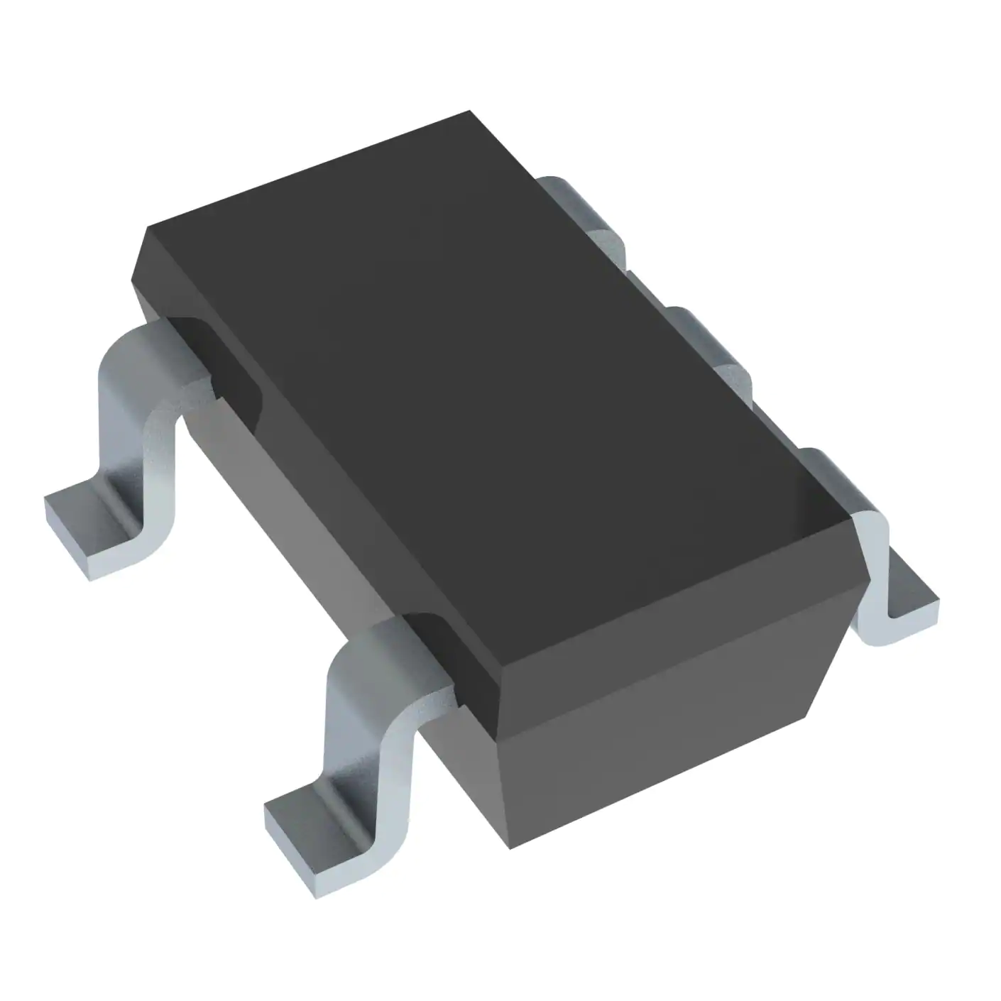
SOT23-5 (DBV) Package
SOT-5 (DDC) Package
Operating Junction Temperature Range: –40°C to
125°C
The TPS723xx uses a precision voltage reference to
achieve 2% overall accuracy over load, line, and
temperature variations. Available in a small SOT23-5
package, the TPS723xx family is fully specified over
a temperature range of –40°C to 125°C.
Device Information(1)
PART NUMBER
2 Applications
•
•
•
•
•
TPS723xx
Optical Drives
Optical Networking
Noise Sensitive Circuitry
GaAs FET Gate Bias
Video Amplifiers
PACKAGE(2)
BODY SIZE (NOM)
SOT-23 (5)
2.90 mm x 1.60 mm
SOT (5)
2.90 mm x 1.60 mm
(1) For all available packages, see the orderable addendum at
the end of the datasheet.
(2) The two SOT23 packages are identical in size, but the SOT
package is thinner.
Typical Application Circuit
2
IN
OUT
5
2.2 µF
2.2 µF
3
EN
NR
4
10 nF
GND
1
1
An IMPORTANT NOTICE at the end of this data sheet addresses availability, warranty, changes, use in safety-critical applications,
intellectual property matters and other important disclaimers. PRODUCTION DATA.
�TPS72301, TPS72325
SLVS346C – SEPTEMBER 2003 – REVISED SEPTEMBER 2014
www.ti.com
Table of Contents
1
2
3
4
5
6
7
Features ..................................................................
Applications ...........................................................
Description .............................................................
Revision History.....................................................
Pin Configuration and Functions .........................
Specifications.........................................................
1
1
1
2
3
4
6.1
6.2
6.3
6.4
6.5
6.6
4
4
4
4
5
6
Absolute Maximum Ratings ......................................
Handling Ratings.......................................................
Recommended Operating Conditions.......................
Thermal Information ..................................................
Electrical Characteristics...........................................
Typical Characteristics ..............................................
Detailed Description ............................................ 11
7.1
7.2
7.3
7.4
Overview .................................................................
Functional Block Diagrams .....................................
Feature Description.................................................
Device Functional Modes........................................
11
11
12
12
8
Application and Implementation ........................ 13
8.1 Application Information............................................ 13
8.2 Typical Application .................................................. 13
8.3 Do's and Don'ts ....................................................... 14
9 Power-Supply Recommendations...................... 15
10 Layout................................................................... 15
10.1
10.2
10.3
10.4
Layout Guidelines .................................................
Layout Example ....................................................
Power Dissipation .................................................
Thermal Protection................................................
15
15
15
15
11 Device and Documentation Support ................. 16
11.1
11.2
11.3
11.4
11.5
Device Support......................................................
Related Links ........................................................
Trademarks ...........................................................
Electrostatic Discharge Caution ............................
Glossary ................................................................
16
16
16
16
16
12 Mechanical, Packaging, and Orderable
Information ........................................................... 16
4 Revision History
Changes from Revision B (July 2007) to Revision C
Page
•
Changed format to meet latest data sheet standards; added new sections, and moved existing sections .......................... 1
•
Added bullet item for DDC package to Features list ............................................................................................................. 1
•
Revised Device Information table to include SOT-5 package ................................................................................................ 1
•
Updated Typical Application Circuit to show SOT-5 (DDC) package pin configuration ......................................................... 1
•
Added pin configuration drawings ......................................................................................................................................... 3
•
Deleted Dissipation Ratings table; see Thermal Information ................................................................................................ 4
•
Changed y-axis title in Figure 11 to Feedback Current from Supply Current ....................................................................... 6
•
Reworded second paragraph in Current Limit subsection. .................................................................................................. 12
Changes from Revision A (June 2007) to Revision B
Page
•
Added second paragraph in Current Limit subsection ........................................................................................................ 12
•
Changed equation shown in Figure 27 ................................................................................................................................ 13
Changes from Original (September 2003) to Revision A
Page
•
Changed document format to correspond to current product line standards ......................................................................... 1
•
Removed Output Voltage vs Output Current graph (original Fig 2) ...................................................................................... 6
2
Submit Documentation Feedback
Copyright © 2003–2014, Texas Instruments Incorporated
Product Folder Links: TPS72301 TPS72325
�TPS72301, TPS72325
www.ti.com
SLVS346C – SEPTEMBER 2003 – REVISED SEPTEMBER 2014
5 Pin Configuration and Functions
DBV PACKAGE
SOT23-5
Top View
5
GND
1
IN
2
EN
3
4
DDC PACKAGE
SOT-5
Top View
OUT
GND
1
IN
2
EN
3
NR/FB
5
OUT
4
NR/FB
Pin Functions
PIN
I/O
DESCRIPTION
NAME
NO.
GND
1
—
IN
2
I
Input supply
EN
3
I
Bipolar enable pin. Driving this pin above the positive enable threshold or below the negative enable
threshold turns on the regulator. Driving this pin below the positive disable threshold and above the
negative disable threshold puts the regulator into shutdown mode.
NR
4
—
Fixed voltage versions only. Connecting an external capacitor between this pin and ground, bypasses
noise generated by the internal bandgap. This configuration allows output noise to be reduced to very
low levels.
FB
4
I
Adjustable voltage version only. This pin is the input to the control loop error amplifier. It is used to set
the output voltage of the device.
OUT
5
O
Regulated output voltage. A small, 2.2-μF ceramic capacitor is needed from this pin to GND to ensure
stability.
Ground
Copyright © 2003–2014, Texas Instruments Incorporated
Product Folder Links: TPS72301 TPS72325
Submit Documentation Feedback
3
�TPS72301, TPS72325
SLVS346C – SEPTEMBER 2003 – REVISED SEPTEMBER 2014
www.ti.com
6 Specifications
6.1 Absolute Maximum Ratings
over operating junction temperature range (unless otherwise noted) (1) (2)
Voltage
Current
MIN
MAX
UNIT
IN
–11
+0.3
V
NR
–11
+5.5
V
EN
–VI
+5.5
V
OUT
–11
+0.3
V
OUT
Internally limited
Output short-circuit duration
See Thermal Information
table
Continuous total power dissipation
Operating junction temperature, TJ
(1)
(2)
A
Indefinite
–65
150
°C
Stresses beyond those listed under Absolute Maximum Ratings may cause permanent damage to the device. These are stress ratings
only, which do not imply functional operation of the device at these or any other conditions beyond those indicated under Recommended
Operating Conditions. Exposure to absolute-maximum-rated conditions for extended periods may affect device reliability.
All voltage values are with respect to network ground terminal.
6.2 Handling Ratings
Tstg
MIN
MAX
UNIT
–65
150
°C
Human body model (HBM), per ANSI/ESDA/JEDEC JS-001, all
pins
–1000
1000
Charged device model (CDM), per JEDEC specification
JESD22-C101, all pins
–500
500
Storage temperature range
V(ESD)
Electrostatic discharge
V
6.3 Recommended Operating Conditions
over operating junction temperature range (unless otherwise noted)
MIN
VI
Input supply voltage range
IO
Output current
TJ
Operating junction temperature
NOM
MAX
UNIT
–10
–2.7
V
0
200
mA
–40
125
°C
6.4 Thermal Information
TPS723xx
THERMAL METRIC (1)
DBV
DDC
5 PINS
5 PINS
RθJA
Junction-to-ambient thermal resistance
206.9
194.8
RθJC(top)
Junction-to-case (top) thermal resistance
120.5
41.4
RθJB
Junction-to-board thermal resistance
35.9
35.9
ψJT
Junction-to-top characterization parameter
13.3
1.0
ψJB
Junction-to-board characterization parameter
35.0
35.7
RθJC(bot)
Junction-to-case (bottom) thermal resistance
N/A
N/A
(1)
4
UNIT
°C/W
For more information about traditional and new thermal metrics, see the IC Package Thermal Metrics application report, SPRA953.
Submit Documentation Feedback
Copyright © 2003–2014, Texas Instruments Incorporated
Product Folder Links: TPS72301 TPS72325
�TPS72301, TPS72325
www.ti.com
SLVS346C – SEPTEMBER 2003 – REVISED SEPTEMBER 2014
6.5 Electrical Characteristics
Over operating junction temperature range, VI = VO(NOM) – 0.5 V, IO = 1 mA, VEN = 1.5 V, CO = 2.2 μF, and CNR = 0.01 μF,
unless otherwise noted. Typical values are at TJ = 25°C.
TPS723xx
PARAMETER
TEST CONDITIONS
(1)
VI
Input voltage range
VFB
Feedback reference voltage
TPS72301
Output voltage range
TPS72301
Accuracy
TYP
MAX
UNIT
–2.7
V
–1.186
–1.162
V
–10 + VDO
VFB
V
–1%
1%
–10
Nominal
VO
MIN
TPS72325 vs
VI/IO/T
TPS72301 vs
VI/IO/T
TJ = 25°C
TJ = 25°C
–10 V ≤ VI ≤ VO – 0.5 V,
10 μA ≤ IO ≤ 200 mA
–1.210
–2%
±1%
2%
–3%
±1
3%
ΔVO(ΔVI)
Line regulation
–10 V ≤ VI ≤ VO(NOM) – 0.5 V
0.04
%/V
ΔVO(ΔIO)
Load regulation
0 mA ≤ IO ≤ 200 mA
0.002
%/mA
VDO
Dropout voltage at
VO = 0.96 × VO(NOM)
I(LIM)
Current limit
I(GND)
TPS72325
IO = 200 mA
VO = 0.85 × VO(NOM)
Ground pin current
300
280
500
mV
mA
550
800
IO = 0 mA (IQ),
–10 V ≤ VI ≤ VO – 0.5 V
130
200
IO = 200 mA,
–10 V ≤ VI ≤ VO – 0.5 V
350
500
μA
I(SHDN)
Shutdown ground pin current
–0.4 V ≤ VEN ≤ 0.4 V,
–10 V ≤ VI ≤ VO – 0.5 V
0.1
2.0
μA
I(FB)
Feedback pin current
–10 V ≤ VI ≤ VO – 0.5 V
0.05
1.0
μA
PSRR
Power-supply rejection ratio
TPS72325
65
IO = 200 mA, 10 kHz,
CI = CO = 10 μF
48
CO = 10 μF, 10 Hz to 100 kHz,
IO = 200 mA
60
μVRMS
VO = –2.5 V, CO = 1 μF,
RL = 25 Ω
1
ms
dB
Vn
Output noise voltage
tSTR
Startup time
VEN(HI)
Enable threshold positive
VEN(LO)
Enable threshold negative
–1.5
V
VDIS(HI)
Disable threshold positive
0.4
V
VDIS(LO)
Disable threshold negative
I(EN)
Enable pin current
Tsd
Thermal shutdown temperature
TJ
Operating junction temperature
(1)
TPS72325
IO = 200 mA, 1 kHz,
CI = CO = 10 μF
1.5
V
–0.4
V
–10 V ≤ VI ≤ VO – 0.5 V,
–10 V ≤ VEN ≤ ±3.5 V
0.1
Shutdown, temperature increasing
165
Reset, temperature decreasing
145
–40
2.0
μA
°C
125
°C
Maximum VI = (VO – VDO) or – 2.7 V, whichever is more negative.
Copyright © 2003–2014, Texas Instruments Incorporated
Product Folder Links: TPS72301 TPS72325
Submit Documentation Feedback
5
�TPS72301, TPS72325
SLVS346C – SEPTEMBER 2003 – REVISED SEPTEMBER 2014
www.ti.com
6.6 Typical Characteristics
TPS72325 at VI = VO(NOM) – 0.5 V, IO = 1 mA, VEN = 1.5 V, CO = 2.2 μF, and CNR = 0.01 μF, unless otherwise noted.
-2.475
-2.488
TJ = +25°C
TJ = -40°C
-2.500
TJ = +85°C
-2.513
TJ = +125°C
-2.525
-10
VIN = 3V, IOUT = 200mA
Output Voltage, VOUT (V)
Output Voltage (V)
-2.475
-2.488
VIN = 10V, IOUT = 200mA
-2.500
VIN = 10V, IOUT = 0mA
-2.513
VIN = 3V, IOUT = 0mA
-2.525
-9
-8
-7
-6
-5
-4
-3
-2
-40
0
-20
Input Voltage (V)
Figure 1. Output Voltage vs Input Voltage
80
100
120
140
300
TJ = +125°C
Dropout Voltage (mV)
Dropout Voltage (mV)
60
350
300
250
TJ = +25°C
200
150
TJ = -40°C
100
50
TJ = +125°C
250
TJ = +25°C
200
150
TJ = -40°C
100
50
0
0
-10
-9
-8
-7
-6
-5
-4
-3
0
-2
25
50
Input Voltage (V)
75
100
125
150
175
200
Output Current (mA)
Figure 3. TPS72301 Dropout Voltage vs Input Voltage
Figure 4. Dropout Voltage vs Output Current
500
350
450
300
400
Ground Current (mA)
Dropout Voltage (mV)
40
Figure 2. Output Voltage vs Ambient Temperature
350
250
200
150
100
RL = 12.5W
350
300
250
200
150
No Load
100
50
50
0
0
-40
6
20
Ambient Temperature (°C)
-20
0
20
40
60
80
100
120
140
-10
-9
-8
-7
-6
-5
-4
-3
-2
-1
0
Junction Temperature (°C)
Input Voltage (V)
Figure 5. TPS72325 Dropout Voltage vs Junction
Temperature
Figure 6. Ground Current vs Input Voltage
Submit Documentation Feedback
Copyright © 2003–2014, Texas Instruments Incorporated
Product Folder Links: TPS72301 TPS72325
�TPS72301, TPS72325
www.ti.com
SLVS346C – SEPTEMBER 2003 – REVISED SEPTEMBER 2014
Typical Characteristics (continued)
TPS72325 at VI = VO(NOM) – 0.5 V, IO = 1 mA, VEN = 1.5 V, CO = 2.2 μF, and CNR = 0.01 μF, unless otherwise noted.
400
500
450
350
400
300
250
Ground Current (mA)
Ground Current (mA)
TJ = +25°C
TJ = +125°C
200
TJ = -40°C
150
100
VIN = 10V, IOUT = 200mA
350
300
250
200
VIN = 3V, IOUT = 0mA
150
100
50
VIN = 10V, IOUT = 0mA
50
0
0
0
50
100
150
200
-40
0
-20
20
40
60
80
100
120
140
Output Current (mA)
Junction Temperature (°C)
Figure 7. Ground Current vs Output Current
Figure 8. Ground Current vs Junction Temperature
800
250
750
200
Standby Current (nA)
Current Limit (mA)
700
650
600
550
500
450
400
VIN = -10V
150
VIN = -3V
100
50
350
300
0
-40
-20
0
20
40
60
80
100
120
140
-40
-20
0
20
40
60
80
100
120
140
Junction Temperature (°C)
Junction Temperature (°C)
Figure 9. TPS72325 Current Limit vs Junction Temperature
Figure 10. Standby Current vs Junction Temperature
200
1000
800
VOUT = -2.5V
-200
Enable Pin Current (nA)
Feedback Current (nA)
0
-400
-600
-800
-1000
VOUT = -1.2V
-1200
-1400
600
400
200
-200
-600
-1800
-800
-40
-20
0
20
40
60
80
100
120
140
VIN = -10V, VEN = 3.5V
-400
-1600
-2000
VIN = -10V, VEN = -0.5V
0
VIN = -10V, VEN = -10V
-1000
-40
-20
Junction Temperature (°C)
0
20
40
60
80
100
120
140
Ambient Temperature (°C)
Figure 11. TPS72301 Feedback Pin Current vs Junction
Temperature
Figure 12. Enable Pin Current vs Junction Temperature
Copyright © 2003–2014, Texas Instruments Incorporated
Product Folder Links: TPS72301 TPS72325
Submit Documentation Feedback
7
�TPS72301, TPS72325
SLVS346C – SEPTEMBER 2003 – REVISED SEPTEMBER 2014
www.ti.com
Typical Characteristics (continued)
TPS72325 at VI = VO(NOM) – 0.5 V, IO = 1 mA, VEN = 1.5 V, CO = 2.2 μF, and CNR = 0.01 μF, unless otherwise noted.
-2
Minimum Required Input Voltage (V)
Line Regulation (%/V)
Load Regulation (%/mA)
0.25
0.13
Load
0
Line
-0.13
-0.25
-3
TJ = -40°C
-4
-5
-6
TJ = +125°C
-7
-8
-9
-10
-40
0
-20
20
40
60
80
100
120
140
-10
-9
-8
50
0
-50
0
-3.0
CIN = 2.2mF
COUT = 2.2mF
CNR = 0mF
-4.5
0
20
40
60
80
100 120
140 160
-2
CIN = 2.2mF
COUT = 2.2mF
CNR = 0mF
-200
0
20
40
60
80
100 120
140 160
180 200
Time (ms)
Figure 16. TPS72325 Load Transient Response
Output Voltage (mV)
100
0
0
-100
CIN = 2.2mF
COUT = 2.2mF
CNR = 0mF
-200
0
20
40
60
80
100 120
140 160
180 200
Input Voltage (V)
Current Load (mA)
-3
0
-100
180 200
Figure 15. TPS72325 Line Transient Response
DVOUT, Change In
Output Voltage (mV)
-4
0
Time (ms)
CIN = 2.2mF
COUT = 2.2mF
IOUT = 50mA
CNR = 0mF
0
0.1
0.2
Figure 17. TPS72325 Load Transient Response
Submit Documentation Feedback
0.3
0.4
0.5
0.6
0.7
0.8
0.9
1.0
Time (ms)
Time (ms)
8
-5
100
DVOUT, Change In
Output Voltage (mV)
100
-4.0
-6
Figure 14. TPS72301 Minimum Required Input Voltage vs
Output Voltage
Current Load (mA)
Input Voltage (V) Output Voltage (mV)
Figure 13. Line And Load Regulation vs Junction
Temperature
-3.5
-7
Output Voltage (V)
Junction Temperature (°C)
Figure 18. TPS72325 Start-Up Response
Copyright © 2003–2014, Texas Instruments Incorporated
Product Folder Links: TPS72301 TPS72325
�TPS72301, TPS72325
www.ti.com
SLVS346C – SEPTEMBER 2003 – REVISED SEPTEMBER 2014
Typical Characteristics (continued)
0.5
0
0
1
-0.5
2
Voltage (V)
Input Voltage (V)
Output Voltage (mV)
TPS72325 at VI = VO(NOM) – 0.5 V, IO = 1 mA, VEN = 1.5 V, CO = 2.2 μF, and CNR = 0.01 μF, unless otherwise noted.
0
1
CIN = 2.2mF
COUT = 2.2mF
IOUT = 50mA
CNR = 0.01mF
2
3
0
0.1
0.2
0.3
0.4
0.5
0.6
0.7
0.8
0.9
VOUT
VIN
-1.0
-1.5
-2.0
CIN = 2.2mF
COUT = 2.2mF
IOUT = 50mA
CNR = 0mF
-2.5
-3.0
-3.5
1.0
0
1
2
3
4
Time (ms)
Figure 19. TPS72325 Start-Up Response
Total Noise (mVRMS)
COUT = 10mF, IOUT = 100mA
150
COUT = 2.2mF, IOUT = 25mA
100
50
COUT = 10mF, IOUT = 25mA
10
100
9
10
CIN = -2.2mF, COUT = 2.2mF
IOUT = 100mA, CNR = 0.01mF
1k
10k
100k
Time (1ms/div)
CNR (pF)
Figure 22. TPS72325 Output Noise vs Time
Figure 21. TPS72325 Total Noise vs CNR (10 Hz to 100 kHz)
10m
Noise Spectral Density (VRMS/ÖHz)
10m
Noise Spectral Density (VRMS/ÖHz)
8
Figure 20. TPS72325 Power-Up/Power-Down
0
1
7
CIN = 2.2mF
COUT = 2.2mF, IOUT = 100mA
200
6
Output Noise (100mV/div)
250
5
Time (ms)
IOUT = 25mA
1m
IOUT = 100mA
100n
CIN = 0.01mF
COUT = 2.2mF
CNR = 0.01mF
10n
IOUT = 100mA
1m
IOUT = 25mA
100n
CIN = 0mF
COUT = 2.2mF
CNR = 0.01mF
10n
100
1k
10k
100k
100
Frequency (Hz)
1k
10k
100k
Frequency (Hz)
Figure 23. TPS72325 Noise Spectral Density vs Frequency
Figure 24. TPS72325 Noise Spectral Density vs Frequency
Copyright © 2003–2014, Texas Instruments Incorporated
Product Folder Links: TPS72301 TPS72325
Submit Documentation Feedback
9
�TPS72301, TPS72325
SLVS346C – SEPTEMBER 2003 – REVISED SEPTEMBER 2014
www.ti.com
Typical Characteristics (continued)
TPS72325 at VI = VO(NOM) – 0.5 V, IO = 1 mA, VEN = 1.5 V, CO = 2.2 μF, and CNR = 0.01 μF, unless otherwise noted.
90
80
70
IOUT = 100mA
60
IOUT = 1mA
50
40
30
20
10
0
VIN = -5V
CIN = 10mF
COUT = 10mF
CNR = 0mF
IOUT = 200mA
-10
80
70
IOUT = 100mA
60
IOUT = 1mA
50
40
30
20
10
0
VIN = -5V
CIN = 10mF
COUT = 10mF
CNR = 0.01mF
IOUT = 200mA
-10
10
10
Power-Supply Rejection Ratio (dB)
Power-Supply Rejection Ratio (dB)
90
100
1k
10k
100k
1M
10M
10
100
1k
10k
100k
1M
Frequency (Hz)
Frequency (Hz)
Figure 25. PSRR vs Frequency
Figure 26. PSRR vs Frequency
Submit Documentation Feedback
10M
Copyright © 2003–2014, Texas Instruments Incorporated
Product Folder Links: TPS72301 TPS72325
�TPS72301, TPS72325
www.ti.com
SLVS346C – SEPTEMBER 2003 – REVISED SEPTEMBER 2014
7 Detailed Description
7.1 Overview
The TPS723xx is a low-dropout, negative linear voltage regulator with a rated current of 200 mA. It is offered in
trimmed output voltages between –1.5 V and –5.2 V and as an adjustable regulator from –1.2 V to –10 V. It
features very low noise and high power-supply rejection ratio (PSRR), making it ideal for high-sensitivity analog
and RF applications. A shutdown mode is available, reducing ground current to 2 μA maximum over temperature
and process.
7.2 Functional Block Diagrams
TPS72301
IN
OUT
EN
100kW
VREF
1.186V
Current Limit
/Thermal
Protection
5pF
R1
FB
GND
R2
R1 + R2 @ 100kW
TPS72325
IN
OUT
EN
100kW
VREF
1.186V
5pF
Current Limit
/Thermal
Protection
R1
GND
R2
R1 + R2 = 97kW
NR
Copyright © 2003–2014, Texas Instruments Incorporated
Product Folder Links: TPS72301 TPS72325
Submit Documentation Feedback
11
�TPS72301, TPS72325
SLVS346C – SEPTEMBER 2003 – REVISED SEPTEMBER 2014
www.ti.com
7.3 Feature Description
7.3.1 Current Limit
The TPS723xx has internal circuitry that monitors and limits output current to protect the regulator from damage
under all load conditions. When output current reaches the output current limit (550 mA typical), protection
circuitry turns on, reducing output voltage to ensure that current does not increase. See Figure 9 in the Typical
Characteristics section.
Do not drive the output more than 0.3 V above the input. An output voltage more than 0.3 V above the input
voltage biases the body diode in the pass FET, and allows current to flow from the output to the input. This
current is not limited by the device. If this condition is expected, make sure to externally limit the reverse current.
7.3.2 Enable
The enable pin is active above +1.5 V and below –1.5 V, allowing it to be controlled by a standard TTL signal or
by connection to VI if not used. When driven to GND most internal circuitry is turned off, putting the TPS723xx
into shutdown mode, drawing 2-μA maximum ground current.
7.4 Device Functional Modes
Driving EN over 1.5 V or below –1.5 V turns on the regulator. Driving EN between –1.5 V and +1.5 V puts the
regulator into shutdown mode, thus reducing the operating current to 100 nA, nominal.
12
Submit Documentation Feedback
Copyright © 2003–2014, Texas Instruments Incorporated
Product Folder Links: TPS72301 TPS72325
�TPS72301, TPS72325
www.ti.com
SLVS346C – SEPTEMBER 2003 – REVISED SEPTEMBER 2014
8 Application and Implementation
NOTE
Information in the following applications sections is not part of the TI component
specification, and TI does not warrant its accuracy or completeness. TI’s customers are
responsible for determining suitability of components for their purposes. Customers should
validate and test their design implementation to confirm system functionality.
8.1 Application Information
The TPS723xx family of LDO regulators provides high PSRR and low noise. These features make the family a
good fit for high-sensitivity analog and RF applications.
8.2 Typical Application
The TPS72301 allows designers to specify any output voltage from –10 V to –1.2 V. As shown in the application
circuit in Figure 27, an external resistor divider is used to scale the output voltage (VO) to the reference voltage.
For best accuracy, use precision resistors for R1 and R2. Use the equations in Figure 27 to determine the values
for the resistor divider.
VOUT = –1.186 1 +
R1
R2
R1+R2 ≈ 100kΩ
2
5
IN
OUT
R1
4
3
FB
EN
GND
R2
1
Figure 27. TPS72301 Adjustable LDO Regulator Programming
8.2.1 Design Requirements
8.2.1.1 Capacitor Selection for Stability
Appropriate input and output capacitors should be used for the intended application. The TPS723xx only requires
a 2.2-μF ceramic output capacitor to be used for stable operation. Both the capacitor value and equivalent series
resistance (ESR) affect stability, output noise, PSRR, and transient response. For typical applications, a 2.2-μF
ceramic output capacitor located close to the regulator is sufficient.
8.2.1.2 Output Noise
Without external bypassing, output noise of the TPS723xx from 10 Hz to 100 kHz is 200 μVRMS typical. The
dominant contributor to output noise is the internal bandgap reference. Adding an external 0.01-μF capacitor to
ground reduces noise to 60 μVRMS. Best noise performance is achieved using appropriate low ESR capacitors for
bypassing noise at the NR and OUT pins. See Figure 21 in the Typical Characteristics section.
8.2.1.3 Power-Supply Rejection
The TPS723xx offers a very high PSRR for applications with noisy input sources or highly sensitive output supply
lines. For best PSRR, use high-quality input and output capacitors.
8.2.2 Detailed Design Procedure
Select the desired device based on the output voltage.
Provide an input supply with adequate headroom to account for dropout and output current to account for the
GND terminal current, and power the load.
Copyright © 2003–2014, Texas Instruments Incorporated
Product Folder Links: TPS72301 TPS72325
Submit Documentation Feedback
13
�TPS72301, TPS72325
SLVS346C – SEPTEMBER 2003 – REVISED SEPTEMBER 2014
www.ti.com
Typical Application (continued)
8.2.3 Application Curves
0.5
Voltage (V)
-0.5
Output Noise (100mV/div)
VOUT
0
VIN
-1.0
-1.5
-2.0
CIN = 2.2mF
COUT = 2.2mF
IOUT = 50mA
CNR = 0mF
-2.5
-3.0
CIN = -2.2mF, COUT = 2.2mF
IOUT = 100mA, CNR = 0.01mF
-3.5
0
1
2
3
4
5
6
7
8
9
Time (1ms/div)
10
Time (ms)
Figure 29. TPS72325 Output Noise vs Time
Figure 28. TPS72325 Power-Up/Power-Down
Power-Supply Rejection Ratio (dB)
90
80
70
IOUT = 100mA
60
IOUT = 1mA
50
40
30
20
10
0
VIN = -5V
CIN = 10mF
COUT = 10mF
CNR = 0.01mF
IOUT = 200mA
-10
10
100
1k
10k
100k
1M
10M
Frequency (Hz)
Figure 30. PSRR vs Frequency
8.3 Do's and Don'ts
Do place at least one 2.2-µF ceramic capacitor as close as possible to the OUT terminal of the regulator.
Do not place the output capacitor more than 10 mm away from the regulator.
Do connect a 0.1-μF to 2.2-μF low ESR capacitor across the IN terminal and GND input of the regulator.
Do not exceed the absolute maximum ratings.
14
Submit Documentation Feedback
Copyright © 2003–2014, Texas Instruments Incorporated
Product Folder Links: TPS72301 TPS72325
�TPS72301, TPS72325
www.ti.com
SLVS346C – SEPTEMBER 2003 – REVISED SEPTEMBER 2014
9 Power-Supply Recommendations
These devices are designed to operate from an input voltage supply range between –10 V and –2.7 V. The input
voltage range must provide adequate headroom in order for the device to have a regulated output. This input
supply must be well-regulated and stable. If the input supply is noisy, additional input capacitors with low ESR
can help improve the output noise performance.
10 Layout
10.1 Layout Guidelines
To improve ac performance (such as PSRR, output noise, and transient response), design the board with
separate ground planes for VI and VO, with each ground plane connected only at the GND pin of the device. In
addition, connect the bypass capacitor directly to the GND pin of the device.
10.2 Layout Example
CO
Ground
Plane
VO
TPS723
VI
EN
R1
R2
CI
Ground
Plane
Figure 31. Example Layout
10.3 Power Dissipation
The ability to remove heat from the die is different for each package type, presenting different considerations in
the printed circuit board (PCB) layout. The PCB area around the device that is free of other components moves
the head from the device to the ambient air. Performance data for JEDEC low- and high-K boards are given in
the Thermal Information table near the front of this data sheet. Using heavier copper increases the effectiveness
in removing heat from the device. The addition of plated through-holes to heat-dissipating layers also improves
heatsink effectiveness. Power dissipation depends on input voltage and load conditions. Power dissipation is
equal to the product of the output current times the voltage drop across the output pass element, as shown in
Equation 1:
P D + ǒVIN*V OUTǓ @ I OUT
(1)
10.4 Thermal Protection
As protection from damage due to excessive junction temperatures, the TPS723xx has internal protection
circuitry. When junction temperature reaches approximately 165°C, the output device is turned off. After the
device has cooled to 145°C, the output device is enabled, allowing normal operation. For reliable operation,
design is for worst-case junction temperature of ≤ 125°C taking into account worst-case ambient temperature
and load conditions.
Copyright © 2003–2014, Texas Instruments Incorporated
Product Folder Links: TPS72301 TPS72325
Submit Documentation Feedback
15
�TPS72301, TPS72325
SLVS346C – SEPTEMBER 2003 – REVISED SEPTEMBER 2014
www.ti.com
11 Device and Documentation Support
11.1 Device Support
11.1.1 Development Support
11.1.1.1 Spice Models
Computer simulation of circuit performance using SPICE is often useful when analyzing the performance of
analog circuits and systems. A SPICE model for the TPS723xx is available through the product folders under
Simulation Models.
11.1.2 Device Nomenclature
Table 1. Device Nomenclature (1)
PRODUCT
VOUT
TPS723xx yyy z
(1)
XX is nominal output voltage (for example, 25 = 2.5 V, 01 = Adjustable).
YYY is package designator.
Z is package quantity.
For the most current package and ordering information see the Package Option Addendum at the end of this document, or visit the
device product folder at www.ti.com.
11.2 Related Links
The table below lists quick access links. Categories include technical documents, support and community
resources, tools and software, and quick access to sample or buy.
Table 2. Related Links
PARTS
PRODUCT FOLDER
SAMPLE & BUY
TECHNICAL
DOCUMENTS
TOOLS &
SOFTWARE
SUPPORT &
COMMUNITY
TPS72301
Click here
Click here
Click here
Click here
Click here
TPS72325
Click here
Click here
Click here
Click here
Click here
11.3 Trademarks
All trademarks are the property of their respective owners.
11.4 Electrostatic Discharge Caution
These devices have limited built-in ESD protection. The leads should be shorted together or the device placed in conductive foam
during storage or handling to prevent electrostatic damage to the MOS gates.
11.5 Glossary
SLYZ022 — TI Glossary.
This glossary lists and explains terms, acronyms, and definitions.
12 Mechanical, Packaging, and Orderable Information
The following pages include mechanical, packaging, and orderable information. This information is the most
current data available for the designated devices. This data is subject to change without notice and revision of
this document. For browser-based versions of this data sheet, refer to the left-hand navigation.
16
Submit Documentation Feedback
Copyright © 2003–2014, Texas Instruments Incorporated
Product Folder Links: TPS72301 TPS72325
�PACKAGE OPTION ADDENDUM
www.ti.com
28-Feb-2017
PACKAGING INFORMATION
Orderable Device
Status
(1)
Package Type Package Pins Package
Drawing
Qty
Eco Plan
Lead/Ball Finish
MSL Peak Temp
(2)
(6)
(3)
Op Temp (°C)
Device Marking
(4/5)
TPS72301DBVR
ACTIVE
SOT-23
DBV
5
3000
Green (RoHS
& no Sb/Br)
CU NIPDAU
Level-1-260C-UNLIM
-40 to 125
T08I
TPS72301DBVRG4
ACTIVE
SOT-23
DBV
5
3000
Green (RoHS
& no Sb/Br)
CU NIPDAU
Level-1-260C-UNLIM
-40 to 125
T08I
TPS72301DBVT
ACTIVE
SOT-23
DBV
5
250
Green (RoHS
& no Sb/Br)
CU NIPDAU
Level-1-260C-UNLIM
-40 to 125
T08I
TPS72301DBVTG4
ACTIVE
SOT-23
DBV
5
250
Green (RoHS
& no Sb/Br)
CU NIPDAU
Level-1-260C-UNLIM
-40 to 125
T08I
TPS72301DDCR
ACTIVE
SOT-23-THIN
DDC
5
3000
Green (RoHS
& no Sb/Br)
CU NIPDAU
Level-2-260C-1 YEAR
-40 to 125
T08I
TPS72301DDCT
ACTIVE
SOT-23-THIN
DDC
5
250
Green (RoHS
& no Sb/Br)
CU NIPDAU
Level-2-260C-1 YEAR
-40 to 125
T08I
TPS72325DBVR
ACTIVE
SOT-23
DBV
5
3000
Green (RoHS
& no Sb/Br)
CU NIPDAU
Level-1-260C-UNLIM
-40 to 125
T02I
TPS72325DBVRG4
ACTIVE
SOT-23
DBV
5
3000
Green (RoHS
& no Sb/Br)
CU NIPDAU
Level-1-260C-UNLIM
-40 to 125
T02I
TPS72325DBVT
ACTIVE
SOT-23
DBV
5
250
Green (RoHS
& no Sb/Br)
CU NIPDAU
Level-1-260C-UNLIM
-40 to 125
T02I
TPS72325DBVTG4
ACTIVE
SOT-23
DBV
5
250
Green (RoHS
& no Sb/Br)
CU NIPDAU
Level-1-260C-UNLIM
-40 to 125
T02I
(1)
The marketing status values are defined as follows:
ACTIVE: Product device recommended for new designs.
LIFEBUY: TI has announced that the device will be discontinued, and a lifetime-buy period is in effect.
NRND: Not recommended for new designs. Device is in production to support existing customers, but TI does not recommend using this part in a new design.
PREVIEW: Device has been announced but is not in production. Samples may or may not be available.
OBSOLETE: TI has discontinued the production of the device.
(2)
Eco Plan - The planned eco-friendly classification: Pb-Free (RoHS), Pb-Free (RoHS Exempt), or Green (RoHS & no Sb/Br) - please check http://www.ti.com/productcontent for the latest availability
information and additional product content details.
TBD: The Pb-Free/Green conversion plan has not been defined.
Pb-Free (RoHS): TI's terms "Lead-Free" or "Pb-Free" mean semiconductor products that are compatible with the current RoHS requirements for all 6 substances, including the requirement that
lead not exceed 0.1% by weight in homogeneous materials. Where designed to be soldered at high temperatures, TI Pb-Free products are suitable for use in specified lead-free processes.
Pb-Free (RoHS Exempt): This component has a RoHS exemption for either 1) lead-based flip-chip solder bumps used between the die and package, or 2) lead-based die adhesive used between
the die and leadframe. The component is otherwise considered Pb-Free (RoHS compatible) as defined above.
Green (RoHS & no Sb/Br): TI defines "Green" to mean Pb-Free (RoHS compatible), and free of Bromine (Br) and Antimony (Sb) based flame retardants (Br or Sb do not exceed 0.1% by weight
in homogeneous material)
Addendum-Page 1
Samples
�PACKAGE OPTION ADDENDUM
www.ti.com
28-Feb-2017
(3)
MSL, Peak Temp. - The Moisture Sensitivity Level rating according to the JEDEC industry standard classifications, and peak solder temperature.
(4)
There may be additional marking, which relates to the logo, the lot trace code information, or the environmental category on the device.
(5)
Multiple Device Markings will be inside parentheses. Only one Device Marking contained in parentheses and separated by a "~" will appear on a device. If a line is indented then it is a continuation
of the previous line and the two combined represent the entire Device Marking for that device.
(6)
Lead/Ball Finish - Orderable Devices may have multiple material finish options. Finish options are separated by a vertical ruled line. Lead/Ball Finish values may wrap to two lines if the finish
value exceeds the maximum column width.
Important Information and Disclaimer:The information provided on this page represents TI's knowledge and belief as of the date that it is provided. TI bases its knowledge and belief on information
provided by third parties, and makes no representation or warranty as to the accuracy of such information. Efforts are underway to better integrate information from third parties. TI has taken and
continues to take reasonable steps to provide representative and accurate information but may not have conducted destructive testing or chemical analysis on incoming materials and chemicals.
TI and TI suppliers consider certain information to be proprietary, and thus CAS numbers and other limited information may not be available for release.
In no event shall TI's liability arising out of such information exceed the total purchase price of the TI part(s) at issue in this document sold by TI to Customer on an annual basis.
OTHER QUALIFIED VERSIONS OF TPS723 :
• Automotive: TPS723-Q1
NOTE: Qualified Version Definitions:
• Automotive - Q100 devices qualified for high-reliability automotive applications targeting zero defects
Addendum-Page 2
�PACKAGE MATERIALS INFORMATION
www.ti.com
17-Jan-2019
TAPE AND REEL INFORMATION
*All dimensions are nominal
Device
Package Package Pins
Type Drawing
SPQ
TPS72301DBVR
SOT-23
3000
180.0
8.4
DBV
5
Reel
Reel
A0
Diameter Width (mm)
(mm) W1 (mm)
B0
(mm)
K0
(mm)
P1
(mm)
W
Pin1
(mm) Quadrant
3.2
3.2
1.4
4.0
8.0
Q3
TPS72301DBVT
SOT-23
DBV
5
250
180.0
8.4
3.2
3.2
1.4
4.0
8.0
Q3
TPS72301DDCR
SOT23-THIN
DDC
5
3000
179.0
8.4
3.2
3.2
1.4
4.0
8.0
Q3
TPS72301DDCT
SOT23-THIN
DDC
5
250
180.0
8.4
3.2
3.2
1.4
4.0
8.0
Q3
TPS72325DBVR
SOT-23
DBV
5
3000
179.0
8.4
3.2
3.2
1.4
4.0
8.0
Q3
TPS72325DBVT
SOT-23
DBV
5
250
180.0
8.4
3.2
3.2
1.4
4.0
8.0
Q3
Pack Materials-Page 1
�PACKAGE MATERIALS INFORMATION
www.ti.com
17-Jan-2019
*All dimensions are nominal
Device
Package Type
Package Drawing
Pins
SPQ
Length (mm)
Width (mm)
Height (mm)
TPS72301DBVR
SOT-23
DBV
5
3000
203.0
203.0
35.0
TPS72301DBVT
SOT-23
DBV
5
250
203.0
203.0
35.0
TPS72301DDCR
SOT-23-THIN
DDC
5
3000
195.0
200.0
45.0
TPS72301DDCT
SOT-23-THIN
DDC
5
250
195.0
200.0
45.0
TPS72325DBVR
SOT-23
DBV
5
3000
203.0
203.0
35.0
TPS72325DBVT
SOT-23
DBV
5
250
203.0
203.0
35.0
Pack Materials-Page 2
��PACKAGE OUTLINE
DBV0005A
SOT-23 - 1.45 mm max height
SCALE 4.000
SMALL OUTLINE TRANSISTOR
C
3.0
2.6
1.75
1.45
PIN 1
INDEX AREA
1
0.1 C
B
A
5
2X 0.95
1.9
1.45 MAX
3.05
2.75
1.9
2
4
0.5
5X
0.3
0.2
3
(1.1)
C A B
0.15
TYP
0.00
0.25
GAGE PLANE
8
TYP
0
0.22
TYP
0.08
0.6
TYP
0.3
SEATING PLANE
4214839/D 11/2018
NOTES:
1. All linear dimensions are in millimeters. Any dimensions in parenthesis are for reference only. Dimensioning and tolerancing
per ASME Y14.5M.
2. This drawing is subject to change without notice.
3. Refernce JEDEC MO-178.
4. Body dimensions do not include mold flash, protrusions, or gate burrs. Mold flash, protrusions, or gate burrs shall not
exceed 0.15 mm per side.
www.ti.com
�EXAMPLE BOARD LAYOUT
DBV0005A
SOT-23 - 1.45 mm max height
SMALL OUTLINE TRANSISTOR
PKG
5X (1.1)
1
5
5X (0.6)
SYMM
(1.9)
2
2X (0.95)
3
4
(R0.05) TYP
(2.6)
LAND PATTERN EXAMPLE
EXPOSED METAL SHOWN
SCALE:15X
SOLDER MASK
OPENING
METAL
SOLDER MASK
OPENING
METAL UNDER
SOLDER MASK
EXPOSED METAL
EXPOSED METAL
0.07 MIN
ARROUND
0.07 MAX
ARROUND
NON SOLDER MASK
DEFINED
(PREFERRED)
SOLDER MASK
DEFINED
SOLDER MASK DETAILS
4214839/D 11/2018
NOTES: (continued)
5. Publication IPC-7351 may have alternate designs.
6. Solder mask tolerances between and around signal pads can vary based on board fabrication site.
www.ti.com
�EXAMPLE STENCIL DESIGN
DBV0005A
SOT-23 - 1.45 mm max height
SMALL OUTLINE TRANSISTOR
PKG
5X (1.1)
1
5
5X (0.6)
SYMM
(1.9)
2
2X(0.95)
4
3
(R0.05) TYP
(2.6)
SOLDER PASTE EXAMPLE
BASED ON 0.125 mm THICK STENCIL
SCALE:15X
4214839/D 11/2018
NOTES: (continued)
7. Laser cutting apertures with trapezoidal walls and rounded corners may offer better paste release. IPC-7525 may have alternate
design recommendations.
8. Board assembly site may have different recommendations for stencil design.
www.ti.com
�IMPORTANT NOTICE AND DISCLAIMER
TI PROVIDES TECHNICAL AND RELIABILITY DATA (INCLUDING DATASHEETS), DESIGN RESOURCES (INCLUDING REFERENCE
DESIGNS), APPLICATION OR OTHER DESIGN ADVICE, WEB TOOLS, SAFETY INFORMATION, AND OTHER RESOURCES “AS IS”
AND WITH ALL FAULTS, AND DISCLAIMS ALL WARRANTIES, EXPRESS AND IMPLIED, INCLUDING WITHOUT LIMITATION ANY
IMPLIED WARRANTIES OF MERCHANTABILITY, FITNESS FOR A PARTICULAR PURPOSE OR NON-INFRINGEMENT OF THIRD
PARTY INTELLECTUAL PROPERTY RIGHTS.
These resources are intended for skilled developers designing with TI products. You are solely responsible for (1) selecting the appropriate
TI products for your application, (2) designing, validating and testing your application, and (3) ensuring your application meets applicable
standards, and any other safety, security, or other requirements. These resources are subject to change without notice. TI grants you
permission to use these resources only for development of an application that uses the TI products described in the resource. Other
reproduction and display of these resources is prohibited. No license is granted to any other TI intellectual property right or to any third
party intellectual property right. TI disclaims responsibility for, and you will fully indemnify TI and its representatives against, any claims,
damages, costs, losses, and liabilities arising out of your use of these resources.
TI’s products are provided subject to TI’s Terms of Sale (www.ti.com/legal/termsofsale.html) or other applicable terms available either on
ti.com or provided in conjunction with such TI products. TI’s provision of these resources does not expand or otherwise alter TI’s applicable
warranties or warranty disclaimers for TI products.
Mailing Address: Texas Instruments, Post Office Box 655303, Dallas, Texas 75265
Copyright © 2019, Texas Instruments Incorporated
�


 工商网监
湘ICP备2023018690号
工商网监
湘ICP备2023018690号
