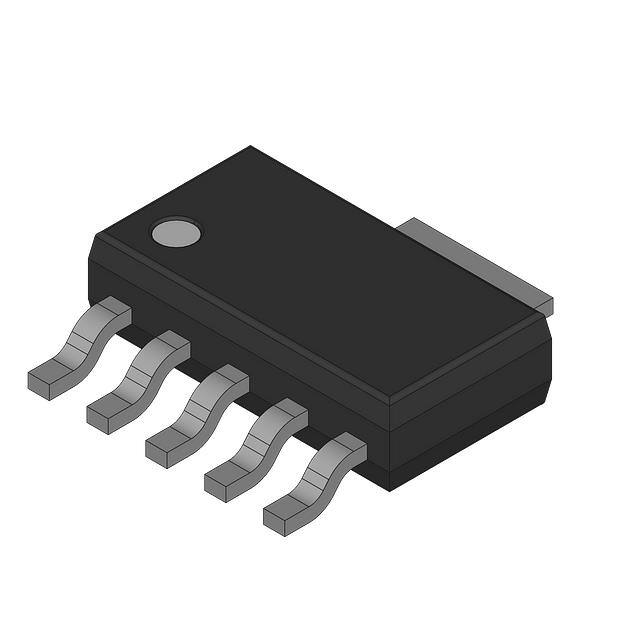
TPS73201-Q1,, TPS73215-Q1,, TPS73216-Q1
TPS73218-Q1, TPS73225-Q1, TPS73230-Q1
TPS73233-Q1, TPS73250-Q1
www.ti.com ........................................................................................................................................................... SGLS303D – MAY 2005 – REVISED MARCH 2009
CAP-FREE NMOS 250-mA LOW-DROPOUT REGULATOR
WITH REVERSE-CURRENT PROTECTION
FEATURES
1
•
•
•
•
•
•
•
•
•
•
•
•
Qualified for Automotive Applications
Stable with No Output Capacitor or Any Value
or Type of Capacitor
Input Voltage Range: 1.7 V to 5.5 V
Ultralow Dropout Voltage:
40 mV Typ at 250 mA
Excellent Load Transient Response—With or
Without Optional Output Capacitor
New NMOS Topology Provides Low Reverse
Leakage Current
Low Noise: 30 µVRMS Typ (10 kHz to 100 kHz)
0.5% Initial Accuracy
1% Overall Accuracy (Line, Load, and
Temperature)
Less Than 1 µA Max IQ in Shutdown Mode
Thermal Shutdown and Specified Min/Max
Current Limit Protection
Available in Multiple Output Voltage Versions
– Fixed Outputs of 1.2 V, 1.5 V, 1.6 V, 1.8 V,
2.5 V, 3 V, 3.3 V, and 5 V
– Adjustable Outputs From 1.2 V to 5.5 V
– Custom Outputs Available
APPLICATIONS
•
•
•
•
Portable/Battery-Powered Equipment
Post-Regulation for Switching Supplies
Noise-Sensitive Circuitry Such as VCOs
Point of Load Regulation for DSPs, FPGAs,
ASICs, and Microprocessors
DESCRIPTION
The TPS732xx family of low-dropout (LDO) voltage
regulators uses a new topology: an NMOS pass
element in a voltage-follower configuration. This
topology is stable using output capacitors with low
ESR, and even allows operation without a capacitor.
It also provides high reverse blockage (low reverse
current) and ground pin current that is nearly constant
over all values of output current.
The TPS732xx uses an advanced BiCMOS process
to yield high precision while delivering low dropout
voltages and low ground pin current. Current
consumption, when not enabled, is under 1 µA and
ideal for portable applications. The extremely low
output noise (30 µVRMS with 0.1 µF CNR) is ideal for
powering VCOs. These devices are protected by
thermal shutdown and foldback current limit.
DRB PACKAGE
(TOP VIEW)
DBV PACKAGE
(TOP VIEW)
IN
1
GND
2
EN
3
5
4
OUT
NR/FB
OUT
NC
NR/FB
GND
1
8
2
7
3
6
4
5
IN
NC
NC
EN
NC – No internal connection
Optional
VIN
Optional
IN
VOUT
OUT
TPS732xx
EN
GND
NR
Optional
Typical Application Circuit for Fixed-Voltage Versions
Figure 1.
1
Please be aware that an important notice concerning availability, standard warranty, and use in critical applications of Texas
Instruments semiconductor products and disclaimers thereto appears at the end of this data sheet.
UNLESS OTHERWISE NOTED this document contains
PRODUCTION DATA information current as of publication date.
Products conform to specifications per the terms of Texas
Instruments standard warranty. Production processing does not
necessarily include testing of all parameters.
Copyright © 2005–2009, Texas Instruments Incorporated
�TPS73201-Q1,, TPS73215-Q1,, TPS73216-Q1
TPS73218-Q1, TPS73225-Q1, TPS73230-Q1
TPS73233-Q1, TPS73250-Q1
SGLS303D – MAY 2005 – REVISED MARCH 2009 ........................................................................................................................................................... www.ti.com
ORDERING INFORMATION (1)
VOUT
(TYP) (2)
TJ
(2)
(3)
(4)
(5)
ORDERABLE PART NUMBER
TOP-SIDE MARKING
Adjustable
or 1.2 V (4)
SOT23-5 – DBV
Reel of 3000
TPS73201QDBVRQ1
PJOQ
VSON-8 – DRB
Reel of 3000
TPS73201QDRBRQ1
PSAQ
1.5 V
SOT23-5 – DBV
Reel of 3000
TPS73215DBVRQ1 (5)
PREVIEW
(5)
PREVIEW
–40°C to 125°C
(1)
PACKAGE (3)
1.6 V
SOT23-5 – DBV
Reel of 3000
TPS73216DBVRQ1
1.8 V
SOT23-5 – DBV
Reel of 3000
TPS73218DBVRQ1 (5)
PREVIEW
2.5 V
SOT23-5 – DBV
Reel of 3000
TPS73225QDBVRQ1
PJNQ
(5)
PREVIEW
3V
SOT23-5 – DBV
Reel of 3000
TPS73230DBVRQ1
3.3 V
SOT23-5 – DBV
Reel of 3000
TPS73233DBVRQ1 (5)
PREVIEW
5V
SOT23-5 – DBV
Reel of 3000
TPS73250DBVRQ1 (5)
PREVIEW
For the most current package and ordering information, see the Package Option Addendum at the end of this document, or see the TI
web site at www.ti.com.
Custom output voltages from 1.3 V to 4 V in 100-mV increments are available on a quick-turn basis for prototyping. Production
quantities are available; minimum order quantities apply. Contact Texas Instruments for details and availability.
Package drawings, thermal data, and symbolization are available at www.ti.com/packaging.
For fixed 1.2-V operation, tie FB to OUT.
Product Preview
ABSOLUTE MAXIMUM RATINGS
over operating junction temperature range unless otherwise noted (1)
TPS732xx
UNIT
VIN range
–0.3 to 6
V
VEN range
–0.3 to 6
V
–0.3 to 5.5
V
VOUT range
Peak output current
Internally limited
Output short-circuit duration
Indefinite
Continuous total power dissipation
See Power Dissipation Ratings
Junction temperature range, TJ
–55 to +150
°C
Storage temperature range
–65 to +150
°C
(2)
(H2) 4
kV
ESD rating, CDM (2)
(C4) 1
kV
(M2) 200
V
ESD rating, HBM
ESD rating, MM (2)
(1)
(2)
Stresses beyond those listed under absolute maximum ratings may cause permanent damage to the device. These are stress ratings
only, and functional operation of the device at these or any other conditions beyond those indicated under the Electrical Characteristics
is not implied. Exposure to absolute maximum rated conditions for extended periods may affect device reliability.
ESD Protection Level per AEC Q100 Classification
POWER DISSIPATION RATINGS (1)
BOARD
PACKAGE
RθJC
RθJA
DERATING FACTOR
ABOVE TA = 25°C
TA ≤ 25°C
POWER RATING
TA = 70°C
POWER RATING
TA = 85°C
POWER RATING
Low-K (2)
DBV
64°C/W
255°C/W
3.9 mW/°C
390 mW
215 mW
155 mW
High-K
(3)
DBV
64°C/W
180°C/W
5.6 mW/°C
560 mW
310 mW
225 mW
High-K
(3)
DRB
1.2°C/W
40°C/W
25.0 mW/°C
2.50 W
1.38 W
1W
(1)
(2)
(3)
2
See Power Dissipation in the Application Information section for more information related to thermal design.
The JEDEC Low-K (1s) board design used to derive this data was a 3 inch x 3 inch, two-layer board with 2-ounce copper traces on top
of the board.
The JEDEC High-K (2s2p) board design used to derive this data was a 3 inch x 3 inch, multilayer board with 1-ounce internal power and
ground planes and 2-ounce copper traces on the top and bottom of the board.
Submit Documentation Feedback
Copyright © 2005–2009, Texas Instruments Incorporated
Product Folder Link(s): TPS73201-Q1 TPS73215-Q1 TPS73216-Q1 TPS73218-Q1 TPS73225-Q1 TPS73230-Q1
TPS73233-Q1 TPS73250-Q1
�TPS73201-Q1,, TPS73215-Q1,, TPS73216-Q1
TPS73218-Q1, TPS73225-Q1, TPS73230-Q1
TPS73233-Q1, TPS73250-Q1
www.ti.com ........................................................................................................................................................... SGLS303D – MAY 2005 – REVISED MARCH 2009
ELECTRICAL CHARACTERISTICS
Over operating temperature range (TJ = –40°C to 125°C), VIN = VOUT(nom) + 0.5 V (1), IOUT = 10 mA, VEN = 1.7 V, and
COUT = 0.1 µF, unless otherwise noted. Typical values are at TJ = 25°C
PARAMETER
TEST CONDITIONS
VIN
Input voltage range (1)
VFB
Internal reference (TPS73201)
Accuracy
VOUT
ΔVOUT%/ΔVIN
TJ = 25°C
TJ = 25°C
VIN, IOUT, and TJ
(VOUT + 0.5 V) ≤ VIN ≤ 5.5 V,
10 mA ≤ IOUT ≤ 250 mA
MAX
V
1.21
V
VFB
5.5–VDO
V
–0.5%
+0.5%
–1%
(VOUT(nom) + 0.5 V) ≤ VIN ≤ 5.5 V
1.2
0.5%
+1%
0.06
1 mA ≤ IOUT ≤ 250 mA
0.002
10 mA ≤ IOUT ≤ 250 mA
0.0008
%/V
ΔVOUT%/ΔIOUT
Load regulation
VDO
Dropout voltage (3)
(VIN = VOUT (nom) – 0.1 V)
IOUT = 250 mA
ZO(DO)
Output impedance in dropout
1.7 V ≤ VIN ≤ (VOUT + VDO)
ICL
Output current limit
VOUT = 0.9 × VOUT(nom)
ISC
Short-circuit current
VOUT = 0 V
300
IREV
Reverse leakage current (4) (–IIN)
VEN ≤ 0.5 V, 0 V ≤ VIN ≤ VOUT
0.1
10
IOUT = 10 mA (IQ)
400
550
IOUT = 250 mA
650
950
0.02
1
40
425
Ground pin current
ISHDN
Shutdown current (IGND)
VEN ≤ 0.5 V, VOUT ≤ VIN ≤ 5.5
PSRR
Power-supply rejection ratio
(ripple rejection)
f = 100 Hz, IOUT = 250 mA
58
f = 10 kHz, IOUT = 250 mA
37
VN
Output noise voltage
BW = 10 Hz – 100 kHz
tSTR
Startup time
VEN(HI)
Enable high (enabled)
VEN(LO)
Enable low (shutdown)
IEN(HI)
Enable pin current (enabled)
TSD
(1)
(2)
(3)
(4)
Thermal shutdown temperature
%/mA
150
mV
600
mA
Ω
0.25
250
IGND
COUT = 10 µF, No CNR
27 × VOUT
COUT= 10 µF, CNR = 0.01 µF
8.5 × VOUT
VOUT = 3 V, RL = 30 Ω
COUT = 1 µF, CNR= 0.01 µF
VEN = 5.5 V
UNIT
5.5
1.198
Nominal
Line regulation (1)
TYP
1.7
Output voltage range (TPS73201) (2)
(1)
MIN
mA
µA
µA
µA
dB
µVRMS
µs
600
1.7
VIN
V
0
0.5
V
0.1
µA
0.02
Shutdown,
Temperature increasing
160
Reset,
Temperature decreasing
140
°C
Minimum VIN = VOUT + VDO or 1.7 V, whichever is greater.
TPS73201 is tested at VOUT = 2.5 V.
VDO is not measured for the TPS73215 or TPS73216, because minimum VIN = 1.7 V.
Fixed-voltage versions only; see the Application Information section for more information.
Copyright © 2005–2009, Texas Instruments Incorporated
Submit Documentation Feedback
Product Folder Link(s): TPS73201-Q1 TPS73215-Q1 TPS73216-Q1 TPS73218-Q1 TPS73225-Q1 TPS73230-Q1
TPS73233-Q1 TPS73250-Q1
3
�TPS73201-Q1,, TPS73215-Q1,, TPS73216-Q1
TPS73218-Q1, TPS73225-Q1, TPS73230-Q1
TPS73233-Q1, TPS73250-Q1
SGLS303D – MAY 2005 – REVISED MARCH 2009 ........................................................................................................................................................... www.ti.com
FUNCTIONAL BLOCK DIAGRAMS
IN
Charge
Pump
EN
Thermal
Protection
Ref
Servo
27kΩ
Bandgap
Error
Amp
Current
Limit
OUT
8kΩ
GND
R1
R1 + R2 = 80kΩ
R2
NR
Figure 2. Fixed Voltage Version
IN
Table 1. Standard 1%
Resistor Values for
Common Output Voltages
VOUT
Charge
Pump
EN
Thermal
Protection
Ref
Servo
27kΩ
Bandgap
Error
Amp
8kΩ
R2
1.2V
Short
Open
1.5V
23.2kΩ
95.3kΩ
1.8V
28.0kΩ
56.2kΩ
2.5V
39.2kΩ
36.5kΩ
2.8V
44.2kΩ
33.2kΩ
3.0V
46.4kΩ
30.9kΩ
3.3V
52.3kΩ
30.1kΩ
5.0V
78.7kΩ
24.9kΩ
OUT
Current
Limit
GND
R1
NOTE: VOUT = (R1 + R2)/R2 × 1.204;
R1R2 ≅ 19kΩ for best
R1
accuracy.
80kΩ
FB
R2
Figure 3. Adjustable Voltage Version
4
Submit Documentation Feedback
Copyright © 2005–2009, Texas Instruments Incorporated
Product Folder Link(s): TPS73201-Q1 TPS73215-Q1 TPS73216-Q1 TPS73218-Q1 TPS73225-Q1 TPS73230-Q1
TPS73233-Q1 TPS73250-Q1
�TPS73201-Q1,, TPS73215-Q1,, TPS73216-Q1
TPS73218-Q1, TPS73225-Q1, TPS73230-Q1
TPS73233-Q1, TPS73250-Q1
www.ti.com ........................................................................................................................................................... SGLS303D – MAY 2005 – REVISED MARCH 2009
PIN ASSIGNMENTS
DRB PACKAGE
(TOP VIEW)
DBV PACKAGE
(TOP VIEW)
IN
1
GND
2
EN
3
5
4
OUT
NR/FB
OUT
NC
NR/FB
GND
1
8
2
7
3
6
4
5
IN
NC
NC
EN
NC – No internal connection
TERMINAL FUNCTIONS
TERMINAL
NAME
NO.
DBV
DESCRIPTION
DRB
IN
1
GND
2
8
Unregulated input supply
EN
3
5
Driving the enable pin (EN) high turns on the regulator. Driving this pin low puts the regulator into shutdown
mode. See the Shutdown section under Applications Information for more details. EN can be connected to IN
if not used.
NR
4
3
Fixed voltage versions only—connecting an external capacitor to this pin bypasses noise generated by the
internal bandgap. This allows output noise to be reduced to low levels.
FB
4
3
Adjustable voltage version only—this is the input to the control loop error amplifier, and is used to set the
output voltage of the device.
NC
—
OUT
5
4, Pad Ground
2, 6, 7 No internal connection
1
Output of the regulator. There are no output capacitor requirements for stability.
Copyright © 2005–2009, Texas Instruments Incorporated
Submit Documentation Feedback
Product Folder Link(s): TPS73201-Q1 TPS73215-Q1 TPS73216-Q1 TPS73218-Q1 TPS73225-Q1 TPS73230-Q1
TPS73233-Q1 TPS73250-Q1
5
�TPS73201-Q1,, TPS73215-Q1,, TPS73216-Q1
TPS73218-Q1, TPS73225-Q1, TPS73230-Q1
TPS73233-Q1, TPS73250-Q1
SGLS303D – MAY 2005 – REVISED MARCH 2009 ........................................................................................................................................................... www.ti.com
TYPICAL CHARACTERISTICS
For all voltage versions at TJ = 25°C, VIN = VOUT(nom) + 0.5 V, IOUT = 10 mA, VEN = 1.7 V, and COUT = 0.1 µF, unless otherwise
noted
LOAD REGULATION
LINE REGULATION
0.5
0.20
Referred to IOUT = 10mA
−40_C
+25_C
+125_C
Change in VOUT (%)
0.3
0.2
0.1
0
−0.1
−0.2
−0.3
Referred to VIN = VOUT + 0.5V at IOUT = 10mA
0.15
Change in VOUT (%)
0.4
0.10
+25_ C
+125_C
0.05
0
−0.05
−40_ C
−0.10
−0.15
−0.4
−0.20
−0.5
0
50
100
150
200
0
250
0.5
1.0
1.5
2.0
2.5
3.0
3.5
4.0
4.5
VIN − VOUT (V)
IOUT (mA)
Figure 4.
Figure 5.
DROPOUT VOLTAGE vs OUTPUT CURRENT
DROPOUT VOLTAGE vs TEMPERATURE
100
100
TPS73225DBV
TPS73225DBV
80
80
VDO (mV)
VDO (mV)
+125_ C
60
+25_ C
40
20
60
50
20
−40_C
0
0
50
100
150
200
0
−50
250
IOUT (mA)
−25
0
25
50
75
100
125
Temperature (_C)
Figure 6.
Figure 7.
OUTPUT VOLTAGE ACCURACY HISTOGRAM
OUTPUT VOLTAGE DRIFT HISTOGRAM
30
18
IOUT = 10mA
16
25
I OUT = 10mA
All Voltage Versions
Percent of Units (%)
Percent of Units (%)
14
20
15
10
12
10
8
6
4
5
2
0
6
−1.0
−0.9
−0.8
−0.7
−0.6
−0.5
−0.4
−0.3
−0.2
−0.1
0
0.1
0.2
0.3
0.4
0.5
0.6
0.7
0.8
0.9
1.0
−100
−90
−80
−70
−60
−50
−40
−30
−20
−10
0
10
20
30
40
50
60
70
80
90
100
0
VOUT Error (%)
Worst Case dVOUT/dT (ppm/_ C)
Figure 8.
Figure 9.
Submit Documentation Feedback
Copyright © 2005–2009, Texas Instruments Incorporated
Product Folder Link(s): TPS73201-Q1 TPS73215-Q1 TPS73216-Q1 TPS73218-Q1 TPS73225-Q1 TPS73230-Q1
TPS73233-Q1 TPS73250-Q1
�TPS73201-Q1,, TPS73215-Q1,, TPS73216-Q1
TPS73218-Q1, TPS73225-Q1, TPS73230-Q1
TPS73233-Q1, TPS73250-Q1
www.ti.com ........................................................................................................................................................... SGLS303D – MAY 2005 – REVISED MARCH 2009
TYPICAL CHARACTERISTICS (continued)
For all voltage versions at TJ = 25°C, VIN = VOUT(nom) + 0.5 V, IOUT = 10 mA, VEN = 1.7 V, and COUT = 0.1 µF, unless otherwise
noted
GROUND PIN CURRENT vs OUTPUT CURRENT
GROUND PIN CURRENT vs TEMPERATURE
1000
800
900
700
IOUT = 250mA
800
600
600
I GND (µA)
I GND (µA)
700
500
400
300
100
50
100
150
200
VIN = 5.5V
VIN = 4V
VIN = 2V
0
−50
250
−25
0
25
50
75
100
IOUT (mA)
Temperature (_C)
Figure 10.
Figure 11.
CURRENT LIMIT vs VOUT
(FOLDBACK)
GROUND PIN CURRENT IN SHUTDOWN
vs TEMPERATURE
500
125
1
450
VENABLE = 0.5V
VIN = VOUT + 0.5V
ICL
400
350
300
IGND (µA)
Current Limit (mA)
300
100
0
0
400
200
VIN = 5.5V
VIN = 4V
VIN = 2V
200
500
ISC
250
200
0.1
150
100
50
TPS73233
0
0
0.5
1.0
1.5
2.0
2.5
3.0
0.01
−50
3.5
0
25
50
Temperature (_C)
Figure 12.
Figure 13.
CURRENT LIMIT vs VIN
75
100
125
CURRENT LIMIT vs TEMPERATURE
600
600
550
550
500
500
Current Limit (mA)
Current Limit (mA)
−25
VOUT (V)
450
400
350
300
450
400
350
300
250
1.5
2.0
2.5
3.0
3.5
4.0
4.5
5.0
5.5
250
−50
−25
0
25
50
VIN (V)
Temperature (_ C)
Figure 14.
Figure 15.
Copyright © 2005–2009, Texas Instruments Incorporated
75
100
Submit Documentation Feedback
Product Folder Link(s): TPS73201-Q1 TPS73215-Q1 TPS73216-Q1 TPS73218-Q1 TPS73225-Q1 TPS73230-Q1
TPS73233-Q1 TPS73250-Q1
125
7
�TPS73201-Q1,, TPS73215-Q1,, TPS73216-Q1
TPS73218-Q1, TPS73225-Q1, TPS73230-Q1
TPS73233-Q1, TPS73250-Q1
SGLS303D – MAY 2005 – REVISED MARCH 2009 ........................................................................................................................................................... www.ti.com
TYPICAL CHARACTERISTICS (continued)
For all voltage versions at TJ = 25°C, VIN = VOUT(nom) + 0.5 V, IOUT = 10 mA, VEN = 1.7 V, and COUT = 0.1 µF, unless otherwise
noted
PSRR (RIPPLE REJECTION) vs FREQUENCY
PSRR (RIPPLE REJECTION) vs VIN – VOUT
40
90
IOUT = 100mA
COUT = Any
80
35
30
IOUT = 1mA
COUT = 10µF
60
50
IO = 100mA
CO = 1µF
IOUT = 1mA
C OUT = Any
40
25
PSRR (dB)
Ripple Rejection (dB)
70
IOUT = 1mA
COUT = 1µF
20
15
30
20
IOUT = Any
COUT = 0µF
10
0
10
100
1k
10k
10
I OUT = 100mA
COUT = 10µF
Frequency = 100kHz
COUT = 10µF
CNR = 0.01µF
5
0
100k
1M
0
10M
0.2
0.4
0.6
0.8
1.0
1.2
1.4
1.6
Frequency (Hz)
VIN − VOUT (V)
Figure 16.
Figure 17.
NOISE SPECTRAL DENSITY
CNR = 0 µF
NOISE SPECTRAL DENSITY
CNR = 0.01 µF
1
1.8
2.0
1
eN (µV/√Hz)
eN (µV/√Hz)
C OUT = 1µF
COUT = 0µF
0.1
COUT = 10µF
COUT = 1µF
0.1
COUT = 0µF
COUT = 10µF
IOUT = 150mA
IOUT = 150mA
0.01
0.01
10
100
1k
10k
100k
10
100
1k
Frequency (Hz)
Frequency (Hz)
Figure 18.
Figure 19.
RMS NOISE VOLTAGE vs COUT
10k
100k
RMS NOISE VOLTAGE vs CNR
60
140
50
120
VOUT = 5.0V
VOUT = 5.0V
100
30
VN (RMS)
VN (RMS)
40
VOUT = 3.3V
20
10
0.1
8
20
CNR = 0.01µF
10Hz < Frequency < 100kHz
1
0
10
VOUT = 3.3V
60
40
VOUT = 1.5V
0
80
VOUT = 1.5V
COUT = 0µF
10Hz < Frequency < 100kHz
1p
10p
100p
COUT (µF)
CNR (F)
Figure 20.
Figure 21.
Submit Documentation Feedback
1n
10n
Copyright © 2005–2009, Texas Instruments Incorporated
Product Folder Link(s): TPS73201-Q1 TPS73215-Q1 TPS73216-Q1 TPS73218-Q1 TPS73225-Q1 TPS73230-Q1
TPS73233-Q1 TPS73250-Q1
�TPS73201-Q1,, TPS73215-Q1,, TPS73216-Q1
TPS73218-Q1, TPS73225-Q1, TPS73230-Q1
TPS73233-Q1, TPS73250-Q1
www.ti.com ........................................................................................................................................................... SGLS303D – MAY 2005 – REVISED MARCH 2009
TYPICAL CHARACTERISTICS (continued)
For all voltage versions at TJ = 25°C, VIN = VOUT(nom) + 0.5 V, IOUT = 10 mA, VEN = 1.7 V, and COUT = 0.1 µF, unless otherwise
noted
TPS73233
LOAD TRANSIENT RESPONSE
VIN = 3.8V
TPS73233
LINE TRANSIENT RESPONSE
COUT = 0µF
50mV/tick
IOUT = 250mA
VOUT
COUT = 0µF
50mV/div
COUT = 1µF
50mV/tick
COUT = 10µF
50mV/tick
VOUT
VOUT
VOUT
C OUT = 100µF
50mV/div
5.5V
250mA
10mA
4.5V
1V/div
VIN
I OUT
10µs/div
10µs/div
Figure 22.
Figure 23.
TPS73233
TURN-ON RESPONSE
TPS73233
TURN-OFF RESPONSE
RL = 1kΩ
COUT = 0µF
RL = 20Ω
COUT = 10µF
VOUT
R L = 20Ω
C OUT = 1µF
R L = 20Ω
C OUT = 1µF
1V/div
RL = 1kΩ
COUT = 0µF
RL = 20Ω
COUT = 10µF
VOUT
2V
2V
VEN
1V/div
1V/div
0V
0V
VEN
100µs/div
100µs/div
Figure 24.
Figure 25.
TPS73233
POWER UP / POWER DOWN
IENABLE vs TEMPERATURE
10
6
5
4
VIN
VOUT
IENABLE (nA)
3
Volts
= 0.5V/µs
dt
50mA/tick
1V/div
VOUT
dVIN
2
1
1
0.1
0
−1
−2
50ms/div
0.01
−50
−25
0
25
50
75
100
125
Temperature (°C)
Figure 26.
Copyright © 2005–2009, Texas Instruments Incorporated
Figure 27.
Submit Documentation Feedback
Product Folder Link(s): TPS73201-Q1 TPS73215-Q1 TPS73216-Q1 TPS73218-Q1 TPS73225-Q1 TPS73230-Q1
TPS73233-Q1 TPS73250-Q1
9
�TPS73201-Q1,, TPS73215-Q1,, TPS73216-Q1
TPS73218-Q1, TPS73225-Q1, TPS73230-Q1
TPS73233-Q1, TPS73250-Q1
SGLS303D – MAY 2005 – REVISED MARCH 2009 ........................................................................................................................................................... www.ti.com
TYPICAL CHARACTERISTICS (continued)
For all voltage versions at TJ = 25°C, VIN = VOUT(nom) + 0.5 V, IOUT = 10 mA, VEN = 1.7 V, and COUT = 0.1 µF, unless otherwise
noted
TPS73201
IFB vs TEMPERATURE
60
160
55
140
50
120
45
100
I FB (nA)
VN (rms)
TPS73201
RMS NOISE VOLTAGE vs CADJ
40
35
30
25
80
60
VOUT = 2.5V
COUT = 0µF
R1 = 39.2kΩ
10Hz < Frequency < 100kHz
20
10p
100p
40
20
1n
10n
0
−50
−25
0
25
50
75
100
CFB (F)
Temperature (_C)
Figure 28.
Figure 29.
TPS73201
LOAD TRANSIENT, ADJUSTABLE VERSION
TPS73201
LINE TRANSIENT, ADJUSTABLE VERSION
CFB = 10nF
R1 = 39.2kΩ
COUT = 0µF
100mV/div
COUT = 0µF
VOUT
100mV/div
VOUT
100mV/div
C OUT = 10µF
100mV/div
125
VOUT = 2.5V
CFB = 10nF
COUT = 10µF
VOUT
VOUT
4.5V
3.5V
250mA
VIN
10mA
10µs/div
Figure 30.
10
Submit Documentation Feedback
IOUT
5µs/div
Figure 31.
Copyright © 2005–2009, Texas Instruments Incorporated
Product Folder Link(s): TPS73201-Q1 TPS73215-Q1 TPS73216-Q1 TPS73218-Q1 TPS73225-Q1 TPS73230-Q1
TPS73233-Q1 TPS73250-Q1
�TPS73201-Q1,, TPS73215-Q1,, TPS73216-Q1
TPS73218-Q1, TPS73225-Q1, TPS73230-Q1
TPS73233-Q1, TPS73250-Q1
www.ti.com ........................................................................................................................................................... SGLS303D – MAY 2005 – REVISED MARCH 2009
APPLICATION INFORMATION
The TPS732xx belongs to a family of new generation LDO regulators that use an NMOS pass transistor to
achieve ultra-low-dropout performance, reverse current blockage, and freedom from output capacitor constraints.
These features, combined with low noise and an enable input, make the TPS732xx ideal for portable
applications. This regulator family offers a wide selection of fixed output voltage versions and an adjustable
output version. All versions have thermal and over-current protection, including foldback current limit.
Figure 32 shows the basic circuit connections for the fixed voltage models. Figure 33 gives the connections for
the adjustable output version (TPS73201).
Optional input capacitor.
May improve source
impedance, noise, or PSRR.
VIN
Optional output capacitor.
May improve load transient,
noise, or PSRR.
IN
VOUT
OUT
TPS732xx
EN
GND
NR
Optional bypass
capacitor to reduce
output noise.
Figure 32. Typical Application Circuit for Fixed-Voltage Versions
Optional input capacitor.
May improve source
impedance, noise, or PSRR.
VIN
IN
Optional output capacitor.
May improve load transient,
noise, or PSRR.
VOUT
OUT
TPS732xx
EN
GND
R1
CFB
FB
R2
VOUT =
(R1 + R2)
× 1.204
R2
Optional capacitor
reduces output noise.
Figure 33. Typical Application Circuit for
Adjustable-Voltage Versions
R1 and R2 can be calculated for any output voltage using the formula shown in Figure 33. Sample resistor values
for common output voltages are shown in Figure 3. For best accuracy, make the parallel combination of R1 and
R2 approximately 19 kΩ.
Input and Output Capacitor Requirements
Although an input capacitor is not required for stability, it is good analog design practice to connect a 0.1-µF to
1-µF low ESR capacitor across the input supply near the regulator. This counteracts reactive input sources and
improves transient response, noise rejection, and ripple rejection. A higher-value capacitor may be necessary if
large, fast rise-time load transients are anticipated or the device is located several inches from the power source.
The TPS732xx does not require an output capacitor for stability and has maximum phase margin with no
capacitor. It is designed to be stable for all available types and values of capacitors. In applications where
VIN – VOUT < 0.5 V and multiple low ESR capacitors are in parallel, ringing may occur when the product of COUT
and total ESR drops below 50 nF. Total ESR includes all parasitic resistances, including capacitor ESR and
board, socket, and solder joint resistance. In most applications, the sum of capacitor ESR and trace resistance
will meet this requirement.
Copyright © 2005–2009, Texas Instruments Incorporated
Submit Documentation Feedback
Product Folder Link(s): TPS73201-Q1 TPS73215-Q1 TPS73216-Q1 TPS73218-Q1 TPS73225-Q1 TPS73230-Q1
TPS73233-Q1 TPS73250-Q1
11
�TPS73201-Q1,, TPS73215-Q1,, TPS73216-Q1
TPS73218-Q1, TPS73225-Q1, TPS73230-Q1
TPS73233-Q1, TPS73250-Q1
SGLS303D – MAY 2005 – REVISED MARCH 2009 ........................................................................................................................................................... www.ti.com
Output Noise
A precision band-gap reference is used to generate the internal reference voltage, VREF. This reference is
dominant noise source within the TPS732xx and it generates approximately 32 µVRMS (10 Hz to 100 kHz) at
reference output (NR). The regulator control loop gains up the reference noise with the same gain as
reference voltage, so that the noise voltage of the regulator is approximately given by:
VOUT
(R1 ) R2)
V N + 32mVRMS
+ 32mVRMS
R2
VREF
Since the value of VREF is 1.2 V, this relationship reduces to:
mV RMS
V N(mVRMS) + 27
V OUT(V)
V
ǒ
Ǔ
the
the
the
(1)
(2)
for the case of no CNR.
An internal 27-kΩ resistor in series with the noise reduction pin (NR) forms a low-pass filter for the voltage
reference when an external noise reduction capacitor, CNR, is connected from NR to ground. For CNR = 10 nF,
the total noise in the 10-Hz to 100-kHz bandwidth is reduced by a factor of ~3.2, giving the approximate
relationship:
ǒmVV Ǔ
V N(mVRMS) + 8.5
RMS
V OUT(V)
(3)
for CNR = 10 nF.
This noise reduction effect is shown as RMS Noise Voltage vs CNR in the Typical Characteristics section.
The TPS73201 adjustable version does not have the noise-reduction pin available. However, connecting a
feedback capacitor, CFB, from the output to the FB pin will reduce output noise and improve load transient
performance.
The TPS732xx uses an internal charge pump to develop an internal supply voltage sufficient to drive the gate of
the NMOS pass element above VOUT. The charge pump generates ~250 µV of switching noise at ~2 MHz;
however, charge-pump noise contribution is negligible at the output of the regulator for most values of IOUT and
COUT.
Board Layout Recommendation to Improve PSRR and Noise Performance
To improve ac performance such as PSRR, output noise, and transient response, it is recommended that the
PCB be designed with separate ground planes for VIN and VOUT, with each ground plane connected only at the
GND pin of the device. In addition, the ground connection for the bypass capacitor should connect directly to the
GND pin of the device.
Internal Current Limit
The TPS732xx internal current limit helps protect the regulator during fault conditions. Foldback helps to protect
the regulator from damage during output short-circuit conditions by reducing current limit when VOUT drops below
0.5 V. See Figure 12 in the Typical Characteristics section for a graph of IOUT vs VOUT.
Shutdown
The Enable pin is active high and is compatible with standard TTL-CMOS levels. VEN below 0.5 V (max) turns
the regulator off and drops the ground pin current to approximately 10 nA. When shutdown capability is not
required, the Enable pin can be connected to VIN. When a pullup resistor is used, and operation down to 1.8 V is
required, use pullup resistor values below 50 kΩ.
12
Submit Documentation Feedback
Copyright © 2005–2009, Texas Instruments Incorporated
Product Folder Link(s): TPS73201-Q1 TPS73215-Q1 TPS73216-Q1 TPS73218-Q1 TPS73225-Q1 TPS73230-Q1
TPS73233-Q1 TPS73250-Q1
�TPS73201-Q1,, TPS73215-Q1,, TPS73216-Q1
TPS73218-Q1, TPS73225-Q1, TPS73230-Q1
TPS73233-Q1, TPS73250-Q1
www.ti.com ........................................................................................................................................................... SGLS303D – MAY 2005 – REVISED MARCH 2009
Dropout Voltage
The TPS732xx uses an NMOS pass transistor to achieve extremely low dropout. When (VIN – VOUT) is less than
the dropout voltage (VDO), the NMOS pass device is in its linear region of operation and the input-to-output
resistance is the RDS-ON of the NMOS pass element.
For large step changes in load current, the TPS732xx requires a larger voltage drop from VIN to VOUT to avoid
degraded transient response. The boundary of this transient dropout region is approximately twice the dc
dropout. Values of VIN – VOUT above this line ensure normal transient response.
Operating in the transient dropout region can cause an increase in recovery time. The time required to recover
from a load transient is a function of the magnitude of the change in load current rate, the rate of change in load
current, and the available headroom (VIN to VOUT voltage drop). Under worst-case conditions [full-scale
instantaneous load change with (VIN – VOUT) close to dc dropout levels], the TPS732xx can take a couple of
hundred microseconds to return to the specified regulation accuracy.
Transient Response
The low open-loop output impedance provided by the NMOS pass element in a voltage follower configuration
allows operation without an output capacitor for many applications. As with any regulator, the addition of a
capacitor (nominal value 1 µF) from the output pin to ground will reduce undershoot magnitude but increase
duration. In the adjustable version, the addition of a capacitor, CFB, from the output to the adjust pin will also
improve the transient response.
The TPS732xx does not have active pulldown when the output is over-voltage. This allows applications that
connect higher voltage sources, such as alternate power supplies, to the output. This also results in an output
overshoot of several percent if the load current quickly drops to zero when a capacitor is connected to the output.
The duration of overshoot can be reduced by adding a load resistor. The overshoot decays at a rate determined
by output capacitor COUT and the internal/external load resistance. The rate of decay is given by:
(Fixed voltage version)
V OUT
dVńdt +
C OUT 80kW
(4)
(Adjustable voltage version)
VOUT
dVńdt +
C OUT 80kW ø (R 1 ) R 2)
(5)
Reverse Current
The NMOS pass element of the TPS732xx provides inherent protection against current flow from the output of
the regulator to the input when the gate of the pass device is pulled low. To ensure that all charge is removed
from the gate of the pass element, the enable pin must be driven low before the input voltage is removed. If this
is not done, the pass element may be left on due to stored charge on the gate.
After the enable pin is driven low, no bias voltage is needed on any pin for reverse current blocking. Note that
reverse current is specified as the current flowing out of the IN pin due to voltage applied on the OUT pin. There
will be additional current flowing into the OUT pin due to the 80-kΩ internal resistor divider to ground (see
Figure 2 and Figure 3).
For the TPS73201, reverse current may flow when VFB is more than 1 V above VIN.
Copyright © 2005–2009, Texas Instruments Incorporated
Submit Documentation Feedback
Product Folder Link(s): TPS73201-Q1 TPS73215-Q1 TPS73216-Q1 TPS73218-Q1 TPS73225-Q1 TPS73230-Q1
TPS73233-Q1 TPS73250-Q1
13
�TPS73201-Q1,, TPS73215-Q1,, TPS73216-Q1
TPS73218-Q1, TPS73225-Q1, TPS73230-Q1
TPS73233-Q1, TPS73250-Q1
SGLS303D – MAY 2005 – REVISED MARCH 2009 ........................................................................................................................................................... www.ti.com
Thermal Protection
Thermal protection disables the output when the junction temperature rises to approximately 160°C, allowing the
device to cool. When the junction temperature cools to approximately 140°C, the output circuitry is again
enabled. Depending on power dissipation, thermal resistance, and ambient temperature, the thermal protection
circuit may cycle on and off. This limits the dissipation of the regulator, protecting it from damage due to
overheating.
Any tendency to activate the thermal protection circuit indicates excessive power dissipation or an inadequate
heatsink. For reliable operation, junction temperature should be limited to 125°C maximum. To estimate the
margin of safety in a complete design (including heatsink), increase the ambient temperature until the thermal
protection is triggered; use worst-case loads and signal conditions. For good reliability, thermal protection should
trigger at least 35°C above the maximum expected ambient condition of your application. This produces a
worst-case junction temperature of 125°C at the highest expected ambient temperature and worst-case load.
The internal protection circuitry of the TPS732xx has been designed to protect against overload conditions. It
was not intended to replace proper heatsinking. Continuously running the TPS732xx into thermal shutdown will
degrade device reliability.
Power Dissipation
The ability to remove heat from the die is different for each package type, presenting different considerations in
the PCB layout. The PCB area around the device that is free of other components moves the heat from the
device to the ambient air. Performance data for JEDEC low- and high-K boards are shown in the Power
Dissipation Ratings table. Using heavier copper will increase the effectiveness in removing heat from the device.
The addition of plated through-holes to heat-dissipating layers will also improve the heat-sink effectiveness.
Power dissipation depends on input voltage and load conditions. Power dissipation is equal to the product of the
output current times the voltage drop across the output pass element (VIN to VOUT):
P D + (VIN * VOUT) I OUT
(6)
Power dissipation can be minimized by using the lowest possible input voltage necessary to assure the required
output voltage.
Package Mounting
Solder pad footprint recommendations for the TPS732xx are presented in the Solder Pad Recommendations for
Surface-Mount Devices (SBFA015) application bulletin, available from the Texas Instruments web site at
www.ti.com.
14
Submit Documentation Feedback
Copyright © 2005–2009, Texas Instruments Incorporated
Product Folder Link(s): TPS73201-Q1 TPS73215-Q1 TPS73216-Q1 TPS73218-Q1 TPS73225-Q1 TPS73230-Q1
TPS73233-Q1 TPS73250-Q1
�PACKAGE OPTION ADDENDUM
www.ti.com
6-Aug-2013
PACKAGING INFORMATION
Orderable Device
Status
(1)
Package Type Package Pins Package
Drawing
Qty
Eco Plan
Lead/Ball Finish
(2)
MSL Peak Temp
Op Temp (°C)
Device Marking
(3)
(4/5)
TPS73201QDBVRQ1
ACTIVE
SOT-23
DBV
5
3000
Green (RoHS
& no Sb/Br)
CU NIPDAU
Level-1-260C-UNLIM
-40 to 125
PJOQ
TPS73201QDRBRQ1
ACTIVE
SON
DRB
8
3000
Green (RoHS
& no Sb/Br)
CU NIPDAU
Level-3-260C-168 HR
-40 to 125
PSAQ
TPS73218QDCQRQ1
PREVIEW
SOT-223
DCQ
6
2500
TBD
Call TI
Call TI
-40 to 125
73218Q
TPS73225QDBVRQ1
OBSOLETE
SOT-23
DBV
5
TBD
Call TI
Call TI
-40 to 125
PJNQ
TPS73250QDCQRQ1
ACTIVE
SOT-223
DCQ
6
Green (RoHS
& no Sb/Br)
CU NIPDAU
Level-3-260C-168 HR
-40 to 125
73250Q
2500
(1)
The marketing status values are defined as follows:
ACTIVE: Product device recommended for new designs.
LIFEBUY: TI has announced that the device will be discontinued, and a lifetime-buy period is in effect.
NRND: Not recommended for new designs. Device is in production to support existing customers, but TI does not recommend using this part in a new design.
PREVIEW: Device has been announced but is not in production. Samples may or may not be available.
OBSOLETE: TI has discontinued the production of the device.
(2)
Eco Plan - The planned eco-friendly classification: Pb-Free (RoHS), Pb-Free (RoHS Exempt), or Green (RoHS & no Sb/Br) - please check http://www.ti.com/productcontent for the latest availability
information and additional product content details.
TBD: The Pb-Free/Green conversion plan has not been defined.
Pb-Free (RoHS): TI's terms "Lead-Free" or "Pb-Free" mean semiconductor products that are compatible with the current RoHS requirements for all 6 substances, including the requirement that
lead not exceed 0.1% by weight in homogeneous materials. Where designed to be soldered at high temperatures, TI Pb-Free products are suitable for use in specified lead-free processes.
Pb-Free (RoHS Exempt): This component has a RoHS exemption for either 1) lead-based flip-chip solder bumps used between the die and package, or 2) lead-based die adhesive used between
the die and leadframe. The component is otherwise considered Pb-Free (RoHS compatible) as defined above.
Green (RoHS & no Sb/Br): TI defines "Green" to mean Pb-Free (RoHS compatible), and free of Bromine (Br) and Antimony (Sb) based flame retardants (Br or Sb do not exceed 0.1% by weight
in homogeneous material)
(3)
MSL, Peak Temp. -- The Moisture Sensitivity Level rating according to the JEDEC industry standard classifications, and peak solder temperature.
(4)
There may be additional marking, which relates to the logo, the lot trace code information, or the environmental category on the device.
(5)
Multiple Device Markings will be inside parentheses. Only one Device Marking contained in parentheses and separated by a "~" will appear on a device. If a line is indented then it is a continuation
of the previous line and the two combined represent the entire Device Marking for that device.
Important Information and Disclaimer:The information provided on this page represents TI's knowledge and belief as of the date that it is provided. TI bases its knowledge and belief on information
provided by third parties, and makes no representation or warranty as to the accuracy of such information. Efforts are underway to better integrate information from third parties. TI has taken and
Addendum-Page 1
Samples
�PACKAGE OPTION ADDENDUM
www.ti.com
6-Aug-2013
continues to take reasonable steps to provide representative and accurate information but may not have conducted destructive testing or chemical analysis on incoming materials and chemicals.
TI and TI suppliers consider certain information to be proprietary, and thus CAS numbers and other limited information may not be available for release.
In no event shall TI's liability arising out of such information exceed the total purchase price of the TI part(s) at issue in this document sold by TI to Customer on an annual basis.
OTHER QUALIFIED VERSIONS OF TPS73201-Q1, TPS73225-Q1, TPS73250-Q1 :
• Catalog: TPS73201, TPS73225, TPS73250
• Enhanced Product: TPS73201-EP, TPS73225-EP, TPS73250-EP
NOTE: Qualified Version Definitions:
• Catalog - TI's standard catalog product
• Enhanced Product - Supports Defense, Aerospace and Medical Applications
Addendum-Page 2
�PACKAGE MATERIALS INFORMATION
www.ti.com
25-Jun-2013
TAPE AND REEL INFORMATION
*All dimensions are nominal
Device
TPS73201QDBVRQ1
Package Package Pins
Type Drawing
SPQ
SOT-23
Reel
Reel
A0
Diameter Width (mm)
(mm) W1 (mm)
DBV
5
3000
179.0
8.4
3.2
B0
(mm)
K0
(mm)
P1
(mm)
W
Pin1
(mm) Quadrant
3.2
1.4
4.0
8.0
Q3
TPS73201QDRBRQ1
SON
DRB
8
3000
330.0
12.4
3.3
3.3
1.1
8.0
12.0
Q2
TPS73250QDCQRQ1
SOT-223
DCQ
6
2500
330.0
12.4
7.1
7.45
1.88
8.0
12.0
Q3
Pack Materials-Page 1
�PACKAGE MATERIALS INFORMATION
www.ti.com
25-Jun-2013
*All dimensions are nominal
Device
Package Type
Package Drawing
Pins
SPQ
Length (mm)
Width (mm)
Height (mm)
TPS73201QDBVRQ1
SOT-23
DBV
5
3000
203.0
203.0
35.0
TPS73201QDRBRQ1
SON
DRB
8
3000
367.0
367.0
35.0
TPS73250QDCQRQ1
SOT-223
DCQ
6
2500
358.0
335.0
35.0
Pack Materials-Page 2
��������IMPORTANT NOTICE
Texas Instruments Incorporated and its subsidiaries (TI) reserve the right to make corrections, enhancements, improvements and other
changes to its semiconductor products and services per JESD46, latest issue, and to discontinue any product or service per JESD48, latest
issue. Buyers should obtain the latest relevant information before placing orders and should verify that such information is current and
complete. All semiconductor products (also referred to herein as “components”) are sold subject to TI’s terms and conditions of sale
supplied at the time of order acknowledgment.
TI warrants performance of its components to the specifications applicable at the time of sale, in accordance with the warranty in TI’s terms
and conditions of sale of semiconductor products. Testing and other quality control techniques are used to the extent TI deems necessary
to support this warranty. Except where mandated by applicable law, testing of all parameters of each component is not necessarily
performed.
TI assumes no liability for applications assistance or the design of Buyers’ products. Buyers are responsible for their products and
applications using TI components. To minimize the risks associated with Buyers’ products and applications, Buyers should provide
adequate design and operating safeguards.
TI does not warrant or represent that any license, either express or implied, is granted under any patent right, copyright, mask work right, or
other intellectual property right relating to any combination, machine, or process in which TI components or services are used. Information
published by TI regarding third-party products or services does not constitute a license to use such products or services or a warranty or
endorsement thereof. Use of such information may require a license from a third party under the patents or other intellectual property of the
third party, or a license from TI under the patents or other intellectual property of TI.
Reproduction of significant portions of TI information in TI data books or data sheets is permissible only if reproduction is without alteration
and is accompanied by all associated warranties, conditions, limitations, and notices. TI is not responsible or liable for such altered
documentation. Information of third parties may be subject to additional restrictions.
Resale of TI components or services with statements different from or beyond the parameters stated by TI for that component or service
voids all express and any implied warranties for the associated TI component or service and is an unfair and deceptive business practice.
TI is not responsible or liable for any such statements.
Buyer acknowledges and agrees that it is solely responsible for compliance with all legal, regulatory and safety-related requirements
concerning its products, and any use of TI components in its applications, notwithstanding any applications-related information or support
that may be provided by TI. Buyer represents and agrees that it has all the necessary expertise to create and implement safeguards which
anticipate dangerous consequences of failures, monitor failures and their consequences, lessen the likelihood of failures that might cause
harm and take appropriate remedial actions. Buyer will fully indemnify TI and its representatives against any damages arising out of the use
of any TI components in safety-critical applications.
In some cases, TI components may be promoted specifically to facilitate safety-related applications. With such components, TI’s goal is to
help enable customers to design and create their own end-product solutions that meet applicable functional safety standards and
requirements. Nonetheless, such components are subject to these terms.
No TI components are authorized for use in FDA Class III (or similar life-critical medical equipment) unless authorized officers of the parties
have executed a special agreement specifically governing such use.
Only those TI components which TI has specifically designated as military grade or “enhanced plastic” are designed and intended for use in
military/aerospace applications or environments. Buyer acknowledges and agrees that any military or aerospace use of TI components
which have not been so designated is solely at the Buyer's risk, and that Buyer is solely responsible for compliance with all legal and
regulatory requirements in connection with such use.
TI has specifically designated certain components as meeting ISO/TS16949 requirements, mainly for automotive use. In any case of use of
non-designated products, TI will not be responsible for any failure to meet ISO/TS16949.
Products
Applications
Audio
www.ti.com/audio
Automotive and Transportation
www.ti.com/automotive
Amplifiers
amplifier.ti.com
Communications and Telecom
www.ti.com/communications
Data Converters
dataconverter.ti.com
Computers and Peripherals
www.ti.com/computers
DLP® Products
www.dlp.com
Consumer Electronics
www.ti.com/consumer-apps
DSP
dsp.ti.com
Energy and Lighting
www.ti.com/energy
Clocks and Timers
www.ti.com/clocks
Industrial
www.ti.com/industrial
Interface
interface.ti.com
Medical
www.ti.com/medical
Logic
logic.ti.com
Security
www.ti.com/security
Power Mgmt
power.ti.com
Space, Avionics and Defense
www.ti.com/space-avionics-defense
Microcontrollers
microcontroller.ti.com
Video and Imaging
www.ti.com/video
RFID
www.ti-rfid.com
OMAP Applications Processors
www.ti.com/omap
TI E2E Community
e2e.ti.com
Wireless Connectivity
www.ti.com/wirelessconnectivity
Mailing Address: Texas Instruments, Post Office Box 655303, Dallas, Texas 75265
Copyright © 2013, Texas Instruments Incorporated
�