���������
�������� �
���������
����������� ����������� ������� ����������
SLVS167C − SEPTEMBER 1998 − REVISED − MAY 1999
D Dual Output Voltages for Split-Supply
D
D
D
D
D
D
D
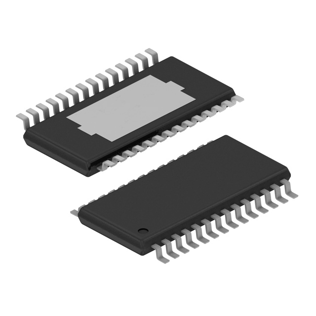
PWP PACKAGE
(TOP VIEW)
Applications
3.3-V/Adjustable Output, 3.3 V/1.8 V, and
3.3 V/2.5
Dropout Voltage < 80 mV Max at
IO = 100 mA (3.3-V option)
Low Quiescent Current, Independent of
Load . . . 340 µA Typ Per Regulator
Ultra-Low-Current Sleep State . . . 2 µA Max
Dual Active-Low Reset Signals with 200-ms
Pulse Width
Output Current Range of 0 mA to 750 mA
Per Regulator
28-Pin PowerPAD TSSOP Package
1
2
3
4
5
6
7
8
9
10
11
12
13
14
NC
NC
1GND
1EN
1IN
1IN
NC
NC
2GND
2EN
2IN
2IN
NC
NC
description
28
27
26
25
24
23
22
21
20
19
18
17
16
15
1RESET
NC
NC
1FB/SENSE
1OUT
1OUT
2RESET
NC
NC
2SENSE
2OUT
2OUT
NC
NC
NC − No internal connection
The TPS73HD3xx family of dual voltage regulators offers very low dropout voltages and dual outputs in a
compact package. Designed primarily for DSP applications, these devices can be used in any mixed-output
voltage application with each regulator supporting up to 750 mA. Output current can be allocated as desired
between the two regulators and used to power many of todays DSPs. Low quiescent current and very low
dropout voltage assure maximum power usage in battery-powered applications. Texas Instruments PowerPAD
TSSOP package allows use of these devices with any voltage/current combination within the range of the listed
specifications without thermal problems, provided proper device mounting procedures are followed. Separate
inputs allow the designer to configure the source power as desired. Dual active-low reset signals allow resetting
of core-logic and I/O separately. Remote sense/feedback terminals provide regulation at the load. The
TPS73HD3xx are available in 28-pin PowerPAD TSSOP. They operate over a free-air temperature range of
−40°C to 125°C.
AVAILABLE OPTIONS
REGULATOR 1
VO (V)
REGULATOR 2
VO (V)
Adj (1.2 − 9.75 V)
3.3 V
TPS73HD301PWPR
1.8 V
3.3 V
TPS73HD318PWPR
2.5 V
3.3 V
TPS73HD325PWPR
TA
−40°C
125°C
−40
C to 125
C
TSSOP
(PWP)
Please be aware that an important notice concerning availability, standard warranty, and use in critical applications of
Texas Instruments semiconductor products and disclaimers thereto appears at the end of this data sheet.
PowerPAD is a trademark of Texas Instruments Incorporated.
Copyright 1999, Texas Instruments Incorporated
���������� ���� �����!"#��� �$ %&��'�# "$ �� (&)*�%"#��� +"#',
���+&%#$ %�����! #� $('%���%"#���$ ('� #-' #'�!$ �� �'."$ ��$#�&!'�#$
$#"�+"�+ /"��"�#0, ���+&%#��� (��%'$$��1 +�'$ ��# �'%'$$"��*0 ��%*&+'
#'$#��1 �� "** ("�"!'#'�$,
POST OFFICE BOX 655303
• DALLAS, TEXAS 75265
1
����������
�������� �
���������
����������� ����������� ������� ����������
SLVS167C − SEPTEMBER 1998 − REVISED − MAY 1999
functional block diagram
IN
†
†
†
EN
−
+
OUT
RESET
Vref = 1.182 V
Delayed
Reset
SENSE/FB
R1
R2
GND
† Switch positions shown with EN low (active).
OUTPUT VOLTAGE
R1
R2
UNIT
Adjustable
0
∞
Ω
1.8 V
122
233
kΩ
2.5 V
260
233
kΩ
3.3 V
420
233
kΩ
Terminal Functions
TERMINAL
NAME
NC
NO.
I/O
1, 2, 7, 8,
13−16, 20,
21, 26, 27
DESCRIPTION
No connection
1GND
3
1EN
4
I
Regulator #1 enable, low = enable
1IN
5, 6
I
Regulator #1 input supply voltage
2GND
9
2EN
10
Regulator #1 ground
Regulator #2 ground
I
Regulator #2 enable, low = enable
2IN
11, 12
I
Regulator #2 input supply voltage
2OUT
17, 18
O
Regulator #2 output voltage
2SENSE
19
I
Regulator #2 output voltage sense (fixed output)
2RESET
22
O
Regulator #2 reset signal, low = reset
23, 24
O
Regulator #1 output voltage
1OUT
1FB/SENSE
25
I
Regulator #1 output voltage feedback (adjustable output)
1RESET
28
O
Regulator #1 reset signal, low = reset
2
POST OFFICE BOX 655303
• DALLAS, TEXAS 75265
����������
�������� �
���������
����������� ����������� ������� ����������
SLVS167C − SEPTEMBER 1998 − REVISED − MAY 1999
absolute maximum ratings over operating free-air temperature (unless otherwise noted)†
Input voltage range, VI (xIN, xRESET, xSENSE, xEN) . . . . . . . . . . . . . . . . . . . . . . . . . . . . . . . . . −0.3 V to 11 V
Differential input voltage,VID (1GND to 2GND) . . . . . . . . . . . . . . . . . . . . . . . . . . . . . . . . . . . . . . . . . . . . . . . . . . 2 V
Output current, IO (1OUT, 2OUT) . . . . . . . . . . . . . . . . . . . . . . . . . . . . . . . . . . . . . . . . . . . . . . . . . . . . . . . . . . . . . 2 A
Continuous total power dissipation . . . . . . . . . . . . . . . . . . . . . . . . . . . . . . . . . . . . See Dissipation Rating Tables
Operating free-air temperature range, TA . . . . . . . . . . . . . . . . . . . . . . . . . . . . . . . . . . . . . . . . . . . −40°C to 125°C
Storage temperature range, Tstg . . . . . . . . . . . . . . . . . . . . . . . . . . . . . . . . . . . . . . . . . . . . . . . . . . . −65°C to 150°C
Lead temperature soldering 1,6 mm (1/16 inch) from case for 10 seconds . . . . . . . . . . . . . . . . . . . . . . . 260°C
† Stresses beyond those listed under “absolute maximum ratings” may cause permanent damage to the device. These are stress ratings only, and
functional operation of the device at these or any other conditions beyond those indicated under “recommended operating conditions” is not
implied. Exposure to absolute-maximum-rated conditions for extended periods may affect device reliability.
NOTE 1: All voltages are with respect to GND.
DISSIPATION RATING TABLE 1 − FREE-AIR TEMPERATURES‡
PACKAGE
PWP‡
AIR FLOW
(CFM)
TA < 25°C
POWER RATING
DERATING FACTOR
ABOVE TA = 25°C
TA = 70°C
POWER RATING
TA = 85°C
POWER RATING
1.5 W
0
2.9 W
23.5 mW/°C
1.9 W
300
4.3 W
34.6 mW/°C
2.8 W
2.2 W
0
3W
23.8 mW/°C
1.9 W
1.5 W
PWP§
300
7.2 W
57.9 mW/°C
4.6 W
3.8 W
‡ This parameter is measured with the recommended copper heat sink pattern on a 1-layer PCB, 5-in × 5-in PCB, 1 oz. copper,
2-in × 2-in coverage (4 in2).
§ This parameter is measured with the recommended copper heat sink pattern on a 8-layer PCB, 1.5-in × 2-in PCB, 1 oz. copper
with layers 1, 2, 4, 5, 7, and 8 at 5% coverage (0.9 in2) and layers 3 and 6 at 100% coverage (6 in2).
recommended operating conditions
Input voltage, VI†
Adjustable output (regulator #1)
3.3−V output (regulator #2)
Input voltage, VI†
High-level input voltage at EN, VIH
MIN
MAX
2.97
10
V
3.97
10
V
2
Low-level input voltage at EN, VIL
Total output current range (per regulator), IO
Operating virtual junction temperature range, TJ
UNIT
V
0.5
V
0
750
mA
−40
125
°C
† Minimum input voltage defined in the recommended operating conditions is the maximum specified output voltage plus dropout voltage, VDO,
at the maximum specified load range (750 mA). Since dropout voltage is a function of output current, the usable range can be extended for lighter
loads. To calculate the minimum input voltage for the maximum load current used in a given application, use the following equation:
V
I(min)
+V
O(max)
)V
DO(max load)
Because regulator 1 of the TPS373HD301 is programmable, rDS(on) should be used to calculate VDO before applying the above equation. The
equation for calculating VDO from rDS(on) is given in Note 3 in the TPS73HD301 electrical characteristics table. The minimum value of 3.5 V is
the absolute lower limit for the recommended input voltage range for the TPS73HD301. With 2.97-V input voltage, the LDO may be in dropout
and will not meet the 3% regulaotr output or 750-mA load current specification.
POST OFFICE BOX 655303
• DALLAS, TEXAS 75265
3
����������
�������� �
���������
����������� ����������� ������� ����������
SLVS167C − SEPTEMBER 1998 − REVISED − MAY 1999
electrical characteristics, VI(IN) = 4.3 V, IO = 10 mA, EN = 0 V, CO = 4.7 µF/CSR‡ = 1 Ω,
SENSE/FB shorted to OUT (unless otherwise noted)
TEST CONDITIONS§
PARAMETER
Quiescent current (active mode), each regulator
TJ
EN ≤ 0.5 V,
0 mA ≤ IO ≤ 750 mA,
See NOTE 2
−40°C to 125°C
−40°C to 125°C
MIN
Supply current (standby mode), each regulator
EN = VI,
NOTE 2
IO
Output current limit, each regulator
VO = 0,
Ilkg
Pass-element leakage current (standby mode)
EN = VI,
See NOTE 2
25°C
VI = 10 V
Output voltage temperature coefficient
MAX
340
415
25°C
550
25°C
ICC
TYP
0.01
2
0.8
1.2
−40°C to 125°C
25°C
0.01
−40°C to 125°C
61
Logic high (EN) (standby mode)
Logic low (EN) (active mode)
See NOTE 2
II
Input current (EN)
0 V ≤ VI ≤ 10 V
−40°C to 125°C
µA
A
ppm/°C
V
2.7
25°C
0.5
0.5
50
25°C
−0.5
−40°C to 125°C
−0.5
0.001
2.05
25°C
0.5
−40°C to 125°C
A
µA
2.5
2.5
1
V
mV
0.5
−40°C to 125°C
IO(RESET) = −300 µA
A
°C
−40°C to 125°C
25°C
Minimum input voltage, for active pass element
µA
A
2
25°C
Minimum input voltage, for valid RESET
75
165
2.5 V ≤ VI ≤ 6 V,
6 V ≤ VI ≤ 10 V
Hysteresis voltage (EN)
0.5
1
−40°C to 125°C
µA
A
2
2
Thermal shutdown junction temperature
Vhys
0.5
UNIT
1.5
1.9
V
V
‡ CSR (compensation series resistance) refers to the total series resistance, including the equivalent series resistance (ESR) of the capacitor,
any series resistance added externally, and PWB trace resistance to CO.
§ Pulse-testing techniques are used to maintain virtual junction temperature as close as possible to ambient temperature; thermal effects must
be taken into account separately.
NOTE 2: Minimum input voltage is 3.5V or Vo(typ) + 1V whichever is greater.
The minimum value of 3.5 V is the absolute lower limit for the recommended input voltage range for the TPS73HD301.
4
POST OFFICE BOX 655303
• DALLAS, TEXAS 75265
����������
�������� �
���������
����������� ����������� ������� ����������
SLVS167C − SEPTEMBER 1998 − REVISED − MAY 1999
electrical characteristics, VI(IN) = 4.3 V, IO = 10 mA, EN = 0 V, CO = 4.7 µF/CSR† = 1 Ω,
SENSE/FB shorted to OUT (unless otherwise noted) (continued)
adjustable regulator
PARAMETER
Reference voltage (1FB)
TEST CONDITIONS‡
5 mA ≤ IO ≤ 750 mA,
See NOTE 2
−40°C to 125°C
Reference voltage temperature coefficient
Pass-element series resistance (see
Note 3)
Input regulation
Output regulation
TJ
25°C
75
0.52
1
−40°C to 125°C
1
ppm/°C
Ω
50 µA ≤ IO ≤ 750 mA
VI = 3.5 V, 50 µA ≤ IO ≤ 750 mA
IO = 5 mA to 750 mA,
See NOTE 2
25°C
0.23
25°C
3
mV
25°C
7
mV
25°C
10
mV
25°C
59
25°C
54
25°C
2
CL = 4.7 µF
25°C
95
CL = 10 µF
25°C
89
CL = 100 µF
25°C
74
IO = 50 µA
IO = 500 mA
f = 120 Hz
Output noise voltage
10 Hz ≤ f ≤ 100 kHz,
CSR = 1 Ω
V(TO)
Trip-threshold voltage (RESET)§
VO(FB) decreasing
Vhys
Hysteresis voltage (RESET)§
Measured at VO(ER)
Input current (1FB)
61
V
0.32
Output noise-spectral density
II
1.217
25°C
f = 120 Hz,
Low-level output voltage (RESET)§
UNIT
50 µA ≤ IO ≤ 750 mA
VI = 3.9 V,
VI = 5.9 V,
f = 120 Hz,
VOL
MAX
1.182
25°C
50 µA ≤ IO ≤ 750 mA,
See NOTE 2
TYP
1.147
−40°C to 125°C
IO = 50 µA to 750 mA,
See NOTE 2
Ripple rejection
MIN
VI = 2.13 V,
−40°C to 125°C
A
IO(RESET) = 400 µA
1.101
dB
mV/√Hz
µV/rms
1.145
25°C
12
25°C
0.1
−40°C to 125°C
mV
0.4
0.4
25°C
−10
−40°C to 125°C
−20
0.1
V
V
10
20
nA
† CSR (compensation series resistance) refers to the total series resistance, including the equivalent series resistance (ESR) of the capacitor,
any series resistance added externally, and PWB trace resistance to CL.
‡ Pulse-testing techniques are used to maintain virtual junction temperature as close as possible to ambient temperature; thermal effects must
be taken into account separately.
§ Output voltage programmed to 2.5 V with closed-loop configuration (see application information)
NOTE 3: To calculate dropout voltage, use equation:
V
DO
+I
O
r
DS(ON)
rDS(ON) is a function of both output current and input voltage. This parametric table lists rDS(ON) for VI = 3.9 V and 5.9 V, which corresponds to
dropout conditions for programmed output voltages of 4 V and 6 V respectively. For other programmed values, refer to Figure 29.
POST OFFICE BOX 655303
• DALLAS, TEXAS 75265
5
����������
�������� �
���������
����������� ����������� ������� ����������
SLVS167C − SEPTEMBER 1998 − REVISED − MAY 1999
electrical characteristics, VI(IN) = 4.3 V, IO = 10 mA, EN = 0 V, CO = 4.7 µF/CSR† = 1 Ω, SENSE/FB
shorted to OUT (unless otherwise noted) (continued)
1.8-V regulator (TPS73HD318)
TEST CONDITIONS‡
PARAMETER
VO
TJ
25°C
MIN
TYP
MAX
1.746
1.8
1.854
−40°C to 125°C
1.728
Output voltage
4.3 V ≤ VI ≤ 10 V
Pass-element series
resistance
(3.5 V − VO)/IO,
IO = 750 mA,
Input regulation
50 µA ≤ IO ≤ 750 mA, See NOTE 2
25°C
6
IO = 5 mA to 750 mA,
IO = 50 µA to 750 mA,
f = 120 Hz,
Output regulation
Ripple rejection
Output noise-spectral density
Output noise voltage
f = 120 Hz,
VI = 3.5 V,
V2SENSE = 0 V§
25°C
0.5
−40°C to 125°C
1
1.2
See NOTE 2
25°C
14
See NOTE 2
25°C
18
IO = 50 µA
IO = 500 mA
25°C
51
25°C
49
f = 120 Hz
10 Hz ≤ f ≤ 100 kHz,
CSR = 1 Ω
1.872
25°C
2
CL = 4.7 µF
25°C
274
CL = 10 µF
25°C
228
CL = 100 µF
25°C
159
UNIT
V
Ω
mV
mV
dB
mV/√Hz
µV/rms
† CSR (compensation series resistance) refers to the total series resistance, including the equivalent series resistance (ESR) of the capacitor, any
series resistance added externally, and PWB trace resistance to CL.
‡ Pulse-testing techniques are used to maintain virtual junction temperature as close as possible to ambient temperature; thermal effects must
be taken into account separately.
§ Pass-element series resistance measured with sense pin disconnected from output to allow output voltge to rise to full saturation.
6
POST OFFICE BOX 655303
• DALLAS, TEXAS 75265
����������
�������� �
���������
����������� ����������� ������� ����������
SLVS167C − SEPTEMBER 1998 − REVISED − MAY 1999
electrical characteristics, VI(IN) = 4.3 V, IO = 10 mA, EN = 0 V, CO = 4.7 µF/CSR† = 1 Ω, SENSE/FB
shorted to OUT (unless otherwise noted) (continued)
2.5-V regulator (TPS73HD325)
TEST CONDITIONS‡
PARAMETER
VO
TJ
25°C
MIN
TYP
2.45
2.5
−40°C to 125°C
2.425
UNIT
2.55
Output voltage
4.3 V ≤ VI ≤ 10 V
Dropout voltage
IO = 750 mA,
VI = 3.5 V
50 µA ≤ IO ≤ 750 mA, See NOTE 2
−40°C to 125°C
25°C
6
mV
IO = 5 mA to 750 mA, See NOTE 2
IO = 50 µA to 750 mA, See NOTE 2
25°C
20
mV
25°C
25
mV
IO = 50 µA
IO = 500 mA
25°C
51
25°C
49
Input regulation
Output regulation
f = 120 Hz,
Ripple rejection
Output noise-spectral density
Output noise voltage
f = 120 Hz,
f = 120 Hz
10 Hz ≤ f ≤ 100 kHz,
CSR = 1 Ω
2.575
800
25°C
2
CL = 4.7 µF
25°C
274
CL = 10 µF
25°C
228
CL = 100 µF
25°C
159
V(TO)
Trip-threshold voltage
(RESET)
Vhys
Hysteresis voltage (RESET)
25°C
18
Low-level output voltage
(RESET)
25°C
0.17
VOL
MAX
VO decreasing
−40°C to 125°C
VI = 2.8 V,
IO(RESET) = −1 mA
V
mV
dB
mV/√Hz
µV/rms
2.172
V
−40°C to 125°C
mV
0.4
0.4
V
† CSR (compensation series resistance) refers to the total series resistance, including the equivalent series resistance (ESR) of the capacitor, any
series resistance added externally, and PWB trace resistance to CL.
‡ Pulse-testing techniques are used to maintain virtual junction temperature as close as possible to ambient temperature; thermal effects must
be taken into account separately.
§ Pass-element series resistance measured with sense pin disconnected from output to allow output voltge to rise to full saturation.
switching characteristics
PARAMETER
Time-out delay (RESET)
TEST CONDITIONS
See Figure 3
POST OFFICE BOX 655303
TJ
25°C
MIN
TYP
MAX
140
200
260
−40°C to 125°C
100
• DALLAS, TEXAS 75265
300
UNIT
ms
7
����������
�������� �
���������
����������� ����������� ������� ����������
SLVS167C − SEPTEMBER 1998 − REVISED − MAY 1999
electrical characteristics, VI(IN) = 4.3 V, IO = 10 mA, EN = 0 V, CO = 4.7 µF/CSR† = 1 Ω, SENSE/FB
shorted to OUT (unless otherwise noted) (continued)
3.3-V regulator (TPS73HD301)
TEST CONDITIONS‡
PARAMETER
VO
Output voltage
4.3 V ≤ VI ≤ 10 V
TJ
25°C
MIN
−40°C to 125°C
3.23
TYP
MAX
UNIT
3.3
3.37
IO = 10 mA,
IO = 100 mA,
VI = 3.23 V
VI = 3.23 V
IO = 750 mA,
VI = 3.23 V
−40°C to 125°C
Pass-element series
resistance
(3.23 V − VO)/IO,
IO = 750 mA
VI = 3.23 V,
25°C
Input regulation
50 µA ≤ IO ≤ 750 mA, See NOTE 2
25°C
6
mV
25°C
30
mV
Output regulation
IO = 5 mA to 750 mA, See NOTE 2
IO = 50 µA to 750 mA, See NOTE 2
25°C
37
mV
IO = 50 µA
IO = 500 mA
25°C
51
25°C
49
Dropout voltage
f = 120 Hz,
Ripple rejection
Output noise-spectral density
Output noise voltage
f = 120 Hz,
4.5
10
25°C
44
100
25°C
353
750
25°C
2
25°C
274
CL = 10 µF
25°C
228
CL = 100 µF
25°C
159
V(TO)
Trip-threshold voltage
(RESET)
Vhys
Hysteresis voltage (RESET)
25°C
18
25°C
0.17
VOL
Low-level output voltage
(RESET)
−40°C to 125°C
VI = 2.8 V,
IO(RESET) = −1 mA
1
1.07
CL = 4.7 µF
VO decreasing
mV
800
0.44
−40°C to 125°C
f = 120 Hz
10 Hz ≤ f ≤ 100 kHz,
CSR = 1 Ω
25°C
V
Ω
dB
mV/√Hz
µV/rms
2.868
V
−40°C to 125°C
mV
0.4
0.4
V
† CSR (compensation series resistance) refers to the total series resistance, including the equivalent series resistance (ESR) of the capacitor, any
series resistance added externally, and PWB trace resistance to CL.
‡ Pulse-testing techniques are used to maintain virtual junction temperature as close as possible to ambient temperature; thermal effects must
be taken into account separately.
switching characteristics
PARAMETER
Time-out delay (RESET)
8
TEST CONDITIONS
See Figure 3
POST OFFICE BOX 655303
TJ
25°C
MIN
TYP
MAX
140
200
260
−40°C to 125°C
100
• DALLAS, TEXAS 75265
300
UNIT
ms
����������
�������� �
���������
����������� ����������� ������� ����������
SLVS167C − SEPTEMBER 1998 − REVISED − MAY 1999
PARAMETER MEASUREMENT INFORMATION
VO
RESET
VI
RESET
IN
VIT+
t
250 kΩ
0.1 µf
OUT
+
EN
VO
10 µF
SENSE
GND
RESET
RESET
Timeout Delay
CSR
t
TEST CIRCUIT
VOLTAGE WAVEFORMS
Figure 1. Test Circuit and Voltage Waveforms
VI
IN
OUT
+
EN
CO
CCER†
SENSE
GND
RL
CSR
† Ceramic capacitor
Figure 2. Test Circuit for Typical Regions of Stability (Refer to Figures 29 through 32)
POST OFFICE BOX 655303
• DALLAS, TEXAS 75265
9
����������
�������� �
���������
����������� ����������� ������� ����������
SLVS167C − SEPTEMBER 1998 − REVISED − MAY 1999
TYPICAL CHARACTERISTICS
Table of Graphs
vs Load current
5
vs Input voltage
6
Adjustable regulator
vs Load current
7
3.3-V regulator
vs Load current
8
Change in dropout voltage
vs Free-air temperature
9
Dropout voltage
vs Output current
10
Change in output voltage
vs Free-air temperature
11
Output voltage
vs Input voltage
12
IQ
Quiescent current
VDO
Dropout voltage
∆VDO
VDO
∆VO
VO
Line regulation
VO
13
Output voltage
vs Output current
Output voltage response from enable (EN)
Load transient response
Line transient response
14, 15
16
Adjustable regulator
17
3.3-V regulator
18
Adjustable regulator
19
3.3-V regulator
20
Ripple rejection
vs Frequency
21
Output spectral noise density
vs Frequency
22
vs Output current
23
vs Added ceramic capacitance
24
vs Output current
25
3.3-V regulator
vs Output current
26
Adjustable regulator
vs Added ceramic capacitance
27
3.3-V regulator
vs Added ceramic capacitance
28
Adjustable regulator
Compensation series resistance (CSR)
rDS(on)
Pass-element resistance
vs Input voltage
29
VI
VIT−
Minimum input voltage for valid RESET
vs Free-air temperature
30
vs Free-air temperature
31
IOL(RESET)
td
RESET output current
vs Input voltage
32
vs Free-air temperature
33
td
Distribution for reset delay
10
Negative-going reset threshold
3.3-V regulato
Reset time delay
34
POST OFFICE BOX 655303
• DALLAS, TEXAS 75265
����������
�������� �
���������
����������� ����������� ������� ����������
SLVS167C − SEPTEMBER 1998 − REVISED − MAY 1999
TYPICAL CHARACTERISTICS
QUIESCENT CURRENT
vs
INPUT VOLTAGE
QUEISCENT CURRENT
vs
LOAD CURRENT
500
500
I Q − Queiscent Current − uA
I Q − Quiescent Current − µ A
Adjustable With VO
Programmed to 2.5 V
400
350
300
TA = 25°C
IO = 500 mA
450
VI = 4.3 V
450
3.3-V Regulator
250
200
150
400
3.3-V Regulator
350
300
250
Adjustable With VO
Programmed to 2.5 V
200
150
100
100
50
50
0
0
0
200
400
600
0
800
1
2
3
4
5
6
7
8
9
10
VI − Input Voltage − V
IO − Load Current − mA
Figure 3
Figure 4
ADJUSTABLE REGULATOR DROPOUT VOLTAGE
vs
LOAD CURRENT
3.3−V REGULATOR DROPOUT VOLTAGE
vs
LOAD CURRENT
0.6
0.6
0.5
0.5
0.4
TA = 125°C
0.3
Dropout Voltage − V
Dropout Voltage − V
TA = 125°C
TA = 25°C
0.2
TA = −40°C
0.1
0.4
TA = 25°C
0.3
0.2
TA = −40°C
0.1
0
0
100
200
300
400
500
600
700
0
0
100
200
300
400
500
600
700
Load Current − mA
Load Current − mA
Figure 5
Figure 6
POST OFFICE BOX 655303
• DALLAS, TEXAS 75265
11
����������
�������� �
���������
����������� ����������� ������� ����������
SLVS167C − SEPTEMBER 1998 − REVISED − MAY 1999
TYPICAL CHARACTERISTICS
CHANGE IN DROPOUT VOLTAGE
vs
FREE-AIR TEMPERATURE
DROPOUT VOLTAGE
vs
OUTPUT CURRENT
1.6
IO = 100 mA
8
TA = 25°C
1.4
6
VDO − Dropout Voltage − V
∆ VDO− Change In Dropout Voltage − mV
10
4
2
0
−2
−4
−6
1.2
1
VI = 3.9 V
0.8
VI = 5.9 V
0.6
VI = 9.65 V
0.4
0.2
−8
−10
−50
−25
0
25
50
75
100
TA − Free-Air Temperature − °C
0
125
0
50
100
150
200
IO − Output Current − mA
Figure 7
Figure 8
OUTPUT VOLTAGE
vs
INPUT VOLTAGE
CHANGE IN OUTPUT VOLTAGE
vs
FREE-AIR TEMPERATURE
6
TA = 25°C
IO = 500 mA
VI = VO(nom) + 1 V
IO = 100 mA
5
10
VO − Output Voltage − V
∆ VO − Change in Output Voltage − mV
20
15
5
0
−5
−10
4
3.3-V Regulator
3
2
2.5 V Regulator and
Adjustable With VO
Programmed to 2.5 V
1
−15
−20
−50
0
−25
0
25
50
75
100
125
0
1
2
3
4
5
Figure 9
Figure 10
POST OFFICE BOX 655303
6
7
VI − Input Voltage − V
TA − Free-Air Temperature − °C
12
250
• DALLAS, TEXAS 75265
8
9
10
����������
�������� �
���������
����������� ����������� ������� ����������
SLVS167C − SEPTEMBER 1998 − REVISED − MAY 1999
TYPICAL CHARACTERISTICS
OUTPUT VOLTAGE
vs
OUTPUT CURRENT
LINE REGULATION
2.55
Adjustable Regulator
TA = 25°C
IO = 250 mA
3.3-V Regulator
15
2.54
2.53
V O − Output voltage − V
10
5
0
−5
2.52
VI = 10 V
2.51
VI = 3.5 V
2.5
2.49
2.48
−10
2.47
−15
2.46
2.45
−20
4
5
8
6
7
VI − Input Voltage − V
9
0
10
200
400
600
800
IO − Output Current − mA
Figure 11
Figure 12
OUTPUT VOLTAGE
vs
OUTPUT CURRENT
3.38
3.3-V Regulator
3.36
V O − Output voltage − V
∆VO− Change In Output Voltage − mV
20
3.34
3.32
3.30
VI = 4.3 V
3.28
VI = 10 V
3.26
3.24
3.22
0
200
400
600
800
IO − Output Current − mA
Figure 13
POST OFFICE BOX 655303
• DALLAS, TEXAS 75265
13
����������
�������� �
���������
����������� ����������� ������� ����������
SLVS167C − SEPTEMBER 1998 − REVISED − MAY 1999
TYPICAL CHARACTERISTICS
6
VO(nom)
4
2
0
TA = 25°C
RL = 500 Ω
Co = 4.7 µF (CSR = 1Ω)
No Input Capacitance
6
4
2
0
EN Voltage − V
VO − Output Voltage − V
OUTPUT VOLTAGE RESPONSE FROM
ENABLE (EN)
−2
0
20
40
60
80 100 120 140
Time − µs
Figure 14
3.3−V REGULATOR
LOAD TRANSIENT RESPONSE
ADJUSTABLE REGULATOR
LOAD TRANSIENT RESPONSE
2000
1000
500
0
−500
TA = 25°C
VI = 6 V
∆IO = 750 mA
Co = 10 µF
CSR = 1 Ohm
tR = 50 ns
−1000
−1500
−2000
−2500
0
100 200 300 400 500 600
∆Vo − Change in Output Voltage − mV
∆Vo − Change in Output Voltage − mV
1500
1500
1000
500
0
−1000
−1500
−2000
0
100 200 300 400 500 600
t − time − us
t − time − us
Figure 16
Figure 15
14
TA = 25°C
VI = 6 V
∆IO = 750 mA
Co = 10 µF
CSR = 1 Ohm
tR = 50 ns
−500
POST OFFICE BOX 655303
• DALLAS, TEXAS 75265
����������
�������� �
���������
����������� ����������� ������� ����������
SLVS167C − SEPTEMBER 1998 − REVISED − MAY 1999
ADJUSTABLE REGULATOR
LINE TRANSIENT RESPONSE
100
50
0
−50
−100
TA = 25°C
CI = 0
Co = 4.7 µF (CSR = 1 Ω)
VO Programmable to 2.5 V
6.5
6.25
6
0
100
200
300
5.75
400
VI − Input Voltage − V
∆VO − Change in Output Voltage − mV
TYPICAL CHARACTERISTICS
t − Time − µs
3.3-V REGULATOR
LINE TRANSIENT RESPONSE
200
100
0
−50
TA = 25°C
CI = 0
Co = 4.7 µF (CSR = 1 Ω)
−100
6.5
6.25
6
0
100
200
300
400
5.75
500
V I − Input Voltage − V
∆VO − Change in Output Voltage − mV
Figure 17
t − Time − µs
Figure 18
POST OFFICE BOX 655303
• DALLAS, TEXAS 75265
15
����������
�������� �
���������
����������� ����������� ������� ����������
SLVS167C − SEPTEMBER 1998 − REVISED − MAY 1999
TYPICAL CHARACTERISTICS
RIPPLE REJECTION
vs
FREQUENCY
OUTPUT SPECTRAL-NOISE DENSITY
vs
FREQUENCY
60
40
TA = 25°C
No Input
Capacitance Added
VI = VO + 1 V
IO = 100 mA
Co = 4.7 µF (CSR = 1)
30
Adjustable With
VO Programmed
to 2.5 V
Ripple Rejection − dB
50
10
Output Spectral-Noise Density − µV/ Hz
3.3-V Regulator
20
10
0
10
100
1K
10 K
100 K
1M
TA = 25°C
No Input Capacitance Added
VI = VO + 1 V
Co = 4.7 µF (CSR = 1 Ω)
1
Co = 10 µF (CSR = 1 Ω)
0.1
Co = 100 µF (CSR = 1 Ω)
0.01
10
10 M
100
f − Frequency − Hz
Figure 19
TYPICAL REGIONS OF STABILITY
TYPICAL REGIONS OF STABILITY
COMPENSATION SERIES RESISTANCE (CSR)†
vs
OUTPUT CURRENT
COMPENSATION SERIES RESISTANCE (CSR)†
vs
ADDED CERAMIC CAPACITANCE
100
CSR − Compensation Series Resistance − Ω
CSR − Compensation Series Resistance − Ω
100 k
Figure 20
100
Region of Instability
10
1
TA = 25°C
VI = VO + 1 V
Co = 4.7 µF
No Added Ceramic Capacitance
No Input Capacitance Added
0.1
Region of Instability
0.01
0
50
100
Region of
Instability
10
TA = 25°C
VI = VO + 1 V
IO = 500 mA
Co = 4.7 µF
No Input Capacitor Added
1
0.1
Region of Instability
0.01
150
200
250
0
0.1
0.2 0.3 0.4 0.5
0.6 0.7 0.8
Added Ceramic Capacitance − µF
IO − Output Current − mA
Figure 21
16
1k
10 k
f − Frequency − Hz
Figure 22
POST OFFICE BOX 655303
• DALLAS, TEXAS 75265
0.9
1
����������
�������� �
���������
����������� ����������� ������� ����������
SLVS167C − SEPTEMBER 1998 − REVISED − MAY 1999
TYPICAL CHARACTERISTICS
ADJUSTABLE REGULATOR TYPICAL REGIONS OF STABILITY
3.3−V REGULATOR TYPICAL REGIONS OF STABILITY
COMPENSATION SERIES RESISTANCE
vs
OUTPUT CURRENT
COMPENSATION SERIES RESISTANCE
vs
OUTPUT CURRENT
100
Region of Instability
10
CSR − Compensation Series Resistance − Ω
CSR − Compensation Series Resistance − Ω
100
TA = 25°C
VI = VO + 1 V
Co = 10 µF
No added ceramic
capacitance.
No input capacitor.
1
0.1
Region of Instability
0.01
Region of Instability
10
TA = 25°C
VI = VO + 1 V
Co = 10 µF
No added ceramic
capacitance.
No input capacitor.
1
0.1
Region of Instability
0.01
0
100
200
300
400
600
500
0
700
100
IO − Output Current − mA
300
400
500
600
700
IO − Output Current − mA
Figure 23
Figure 24
ADJUSTABLE REGULATOR TYPICAL REGIONS OF STABILITY
3.3-V REGULATOR TYPICAL REGIONS OF STABILITY
COMPENSATION SERIES RESISTANCE
vs
ADDED CERAMIC CAPACITANCE
COMPENSATION SERIES RESISTANCE
vs
ADDED CERAMIC CAPACITANCE
100
100
CSR − Compensation Series Resistance − Ω
CSR − Compensation Series Resistance − Ω
200
Region of Instability
10
TA = 25°C
VI = VO + 1 V
IO = 750 mA
Co = 10 µF
No input capacitance.
1
0.1
Region of Instability
0.01
Region of Instability
10
TA = 25°C
VI = VO + 1 V
IO = 750 mA
Co = 10 µF
No input capacitance.
1
0.1
Region of Instability
0.01
0
0.2
0.4
0.6
0.8
1
0
Added Ceramic Capacitance − µF
0.2
0.4
0.6
0.8
1
Added Ceramic Capacitance − µF
Figure 25
Figure 26
POST OFFICE BOX 655303
• DALLAS, TEXAS 75265
17
����������
�������� �
���������
����������� ����������� ������� ����������
SLVS167C − SEPTEMBER 1998 − REVISED − MAY 1999
TYPICAL CHARACTERISTICS
MINIMUM INPUT VOLTAGE FOR VALID RESET
vs
FREE-AIR TEMPERATURE
PASS-ELEMENT RESISTANCE
vs
INPUT VOLTAGE
VI − Minimum Input Voltage For Valid RESET − V
rDS(on) − Pass-Element Resistance − Ω
1.1
TA = 25°C
VI(FB) = 1.12 V
1
0.9
0.8
IO = 500 mA
0.7
0.6
0.5
IO = 100 mA
0.4
0.3
0.2
0.1
2
3
4
9
6
8
5
7
VI − Input Voltage − V
10
ÁÁ
ÁÁ
1.1
1.09
1.08
1.07
1.06
1.05
−50
−25
0
25
50
75
100
TA − Free-Air Temperature − °C
Figure 28
Figure 27
NEGATIVE-GOING RESET THRESHOLD
vs
FREE-AIR TEMPERATURE
RESET OUTPUT CURRENT
vs
INPUT VOLTAGE
4
IL = 10 mA
VOL ≤ 0.4 V
TA = 25°C
3.3-V Regulator
3.5
I OL − RESET Output Current − mA
VIT− − Negative-Going Reset Threshold − mV
15
10
5
0
−5
ÁÁ
ÁÁ
ÁÁ
−10
−15
−50
3
2.5
2
1.5
1
0.5
−25
0
25
50
75
100
125
0
0
1
TA − Free-Air Temperature − °C
2
3
4
5
Figure 30
POST OFFICE BOX 655303
6
7
VI − Input Voltage − V
Figure 29
18
125
• DALLAS, TEXAS 75265
8
9
10
����������
�������� �
���������
����������� ����������� ������� ����������
SLVS167C − SEPTEMBER 1998 − REVISED − MAY 1999
TYPICAL CHARACTERISTICS
RESET DELAY TIME
vs
FREE-AIR TEMPERATURE
DISTRIBUTION FOR RESET DELAY
50
197
TA = 25°C
197 Devices
45
196
Percentage of Units − %
td − Reset Delay Time − ms
40
195
194
193
192
35
30
25
20
15
10
191
5
190
−50
−25
0
25
50
75
100
TA − Free-Air Temperature −°C
0
180
125
185
Figure 31
200
205
190
195
td − Reset Delay Time − ms
210
Figure 32
THERMAL INFORMATION
The TPS73HD3xx is packaged in a high-power dissipation downset lead frame for optimal power handling. with
proper heat dissipation techniques, the full power soutput of these devices can be safely handled over the full
temperture range. The Texas Instruments technical brief, PowerPAD Thermally Enhanced Package (literature
number SLMA002), goes into considerable detail into techniques for properly mounting this type of package for
maximum thermal performance. A thermal conduction plane of approximately 3I y 3I will give a power dissipatio level
of 4.5 W.
Power dissipation within the device can be calculated with the following equation:
P
D
+P
ǒ
Ǔǒ
–P
+V I
)I
– V
IN OUT
I O1
O2
O1
I
O1
POST OFFICE BOX 655303
)V
O2
I
O2
Ǔ
• DALLAS, TEXAS 75265
19
����������
�������� �
���������
����������� ����������� ������� ����������
SLVS167C − SEPTEMBER 1998 − REVISED − MAY 1999
APPLICATION INFORMATION
thermal considerations
DISSIPATION RATING TABLE
PACKAGE
PWP‡
PWP§
AIR FLOW
(CFM)
TA < 25°C
POWER RATING
DERATING FACTOR
ABOVE TA = 25°C
TA = 70°C
POWER RATING
TA = 85°C
POWER RATING
0
2.9 W
23.5 mW/°C
1.9 W
1.5 W
300
4.3 W
34.6 mW/°C
2.8 W
2.2 W
0
3W
23.8 mW/°C
1.9 W
1.5 W
300
7.2 W
57.9 mW/°C
4.6 W
3.8 W
† This parameter is measured with the recommended copper heat sink pattern on a 1-layer PCB, 5-in × 5-in PCB,
1 oz. copper, 2-in × 2-in coverage (4 in2).
‡ This parameter is measured with the recommended copper heat sink pattern on an 8-layer PCB, 1.5-in × 2-in PCB, 1 oz. copper
with layers 1, 2, 4, 5, 7, and 8 at 5% coverage (0.9 in2) and layers 3 and 6 at 100% coverage (6 in2).
The maximum ambient temperature depends on the heatsinking ability of the PCB system. Using the 0 CFM
and 300 CFM data from the dissipation rating table, the derating factor for the PWP package with 6.9 in2 of
copper area on a multilayer PCB is 24 mW/°C and 58 mW/°C respectively. Converting this to ΘJA:
Θ
JA
+
1
Derating
For 0 CFM :
1
+
0.0235
For 300 CFM :
+
+ 42.6°CńW
1
0.0579
+ 17.3°CńW
Given ΘJA, the maximum allowable junction temperature, and the total internal dissipation, the maximum
ambient temperature can be calculated with the following equation. The maximum recommended junction
temperature for the TPS73HD3xx is 150 °C.
ǒ
T Max + T Max * Θ
A
J
JA
P
D
Ǔ
The maximum power dissipation limit is determined using the following equation:
T
D(max)
+
T max * T
J
A
R
θJA
Where:
TJmax is the maximum allowable junction temperature
RθJA is the thermal resistance junction-to-free-air for the package (i.e., 285°C/W for the 5-terminal
SOT-23 package.
TA is the free-air temperautre
The regulator dissipation is calculated using:
P
D
+
ǒVI * VOǓ
1
O
Power dissipation resulting from quiescent current is negligible.
20
POST OFFICE BOX 655303
• DALLAS, TEXAS 75265
����������
�������� �
���������
����������� ����������� ������� ����������
SLVS167C − SEPTEMBER 1998 − REVISED − MAY 1999
APPLICATION INFORMATION
Capitalizing upon the features of the TPS73xx family (low-dropout voltage, low quiescent current, power-saving
shutdown mode, and a supply-voltage supervisor) and the power-dissipation properties of the TSSOP PowerPAD
package has enabled the integration of the TPS73HD3xx dual LDO regulator with high output current for use in DSP
and other multiple voltage applications. Figure 35 shows a typical dual-voltage DSP application.
R2
100 kΩ
R1
100 kΩ
U1
TPS73HD325
2
3
4
5V
5
6
C0
1 µF
7
8
9
10
11
12
13
14
NC
1RESET
NC
NC
1GND
1EN
NC
1FB/SENSE
1IN
1OUT
1IN
1OUT
NC
2RESET
NC
NC
2GND
NC
2EN
2IN
2SENSE
2OUT
2IN
2OUT
NC
NC
NC
NC
28
27
RESET to DSP
26
25
24
23
2.5 V
22
D1
21
20
C3
33 µF
19
+
18
17
DL4148
1
PG
CVdd
(Core
Supply)
D3
DL5817
16
D2
15
3.3 V
C1
1 µF
C2
33 µF
GND
DVdd
(I/O
Supply)
GND
VC549
DSP
Figure 33. Dual-Voltage DSP Application
DSP power requirements include very high transient currents that must be considered in the initial design. This design
uses higher-valued output capacitors to handle the large transient currents. Details of this type of design are shown
in the application report, Designing Power Supplies for TMS320VC549 DSP Systems.
minimum load requirements
The TPS73HD3xx is stable even at zero load; no minimum load is required for operation.
POST OFFICE BOX 655303
• DALLAS, TEXAS 75265
21
����������
�������� �
���������
����������� ����������� ������� ����������
SLVS167C − SEPTEMBER 1998 − REVISED − MAY 1999
APPLICATION INFORMATION
SENSE connection
The SENSE terminal of fixed-output devices must be connected to the regulator output for proper functioning
of the regulator. Normally, this connection should be as short as possible; however, the connection can be made
near a critical circuit (remote sense) to improve performance at that point. Internally, SENSE connects to a
high-impedance wide-bandwidth amplifier through a resistor-divider network, and noise pickup feeds through
to the regulator output. It is essential to route the SENSE connection in such a way as to minimize/avoid noise
pickup. Adding an RC network between SENSE and OUT to filter noise is not recommended because it can
cause the regulator to oscillate.
external capacitor requirements
An input capacitor is not required; however, a ceramic bypass capacitor (0.047 pF to 0.1 µF) improves load
transient response and noise rejection when the TPS73HD3xx is located more than a few inches from the power
supply. A higher-capacitance electrolytic capacitor may be necessary if large (hundreds of milliamps) load
transients with fast rise times are anticipated.
As with most LDO regulators, the TPS73HD3xx requires an output capacitor for stability. A low-ESR 10-µF
solid-tantalum capacitor connected from the regulator output to ground is sufficient to ensure stability over the
full load range (see Figure 44). Adding high-frequency ceramic or film capacitors (such as power-supply bypass
capacitors for digital or analog ICs) can cause the regulator to become unstable unless the ESR of the tantalum
capacitor is less than 1.2 Ω over temperature. Capacitors with published ESR specifications such as the
AVX TPSD106M035R0300 and the Sprague 593D106X0035D2W work well because the maximum ESR at
25°C is 300 mΩ (typically, the ESR in solid-tantalum capacitors increases by a factor of 2 or less when the
temperature drops from 25°C to − 40°C). Where component height and/or mounting area is a problem,
physically smaller, 10-µF devices can be screened for ESR. Figures 23 through 28 show the stable regions of
operation using different values of output capacitance with various values of ceramic load capacitance.
Due to the reduced stability range available when using output capacitors smaller than 10 µF, capacitors in this
range are not recommended. Larger capacitors provide a wider range of stability and better load transient
response. Because capacitor minimum ESR is seldom if ever specified, it may be necessary to add a 0.5-Ω to
1-Ω resistor in series with the capacitor and limit ESR to 1.5 Ω maximum. As shown in the CSR graphs
(Figures 23 through 28), minimum ESR is not a problem when using 10-µF or larger output capacitors.
Below is a partial listing of surface-mount capacitors usable with the TPS73HD3xx. This information, along with
the CSR graphs, is included to assist in selection of suitable capacitance for the user’s application. When
necessary to achieve low height requirements along with high output current and/or high ceramic load
capacitance, several higher ESR capacitors can be used in parallel to meet the guidelines above.
22
POST OFFICE BOX 655303
• DALLAS, TEXAS 75265
����������
�������� �
���������
����������� ����������� ������� ����������
SLVS167C − SEPTEMBER 1998 − REVISED − MAY 1999
APPLICATION INFORMATION
external capacitor requirements (continued)
All load and temperature conditions with up to 1 µF of added ceramic load capacitance:
PART NO.
MFR.
VALUE
MAX ESR†
SIZE (H × L × W)†
T421C226M010AS
Kemet
22 µF, 10 V
0.5
2.8 × 6 × 3.2
593D156X0025D2W
Sprague
15 µF, 25 V
0.3
2.8 × 7.3 × 4.3
593D106X0035D2W
Sprague
10 µF, 35 V
0.3
2.8 × 7.3 × 4.3
10 µF, 35 V
0.3
2.8 × 7.3 × 4.3
TPSD106M035R0300 AVX
Load < 200 mA, ceramic load capacitance < 0.2 µF, full temperature range:
PART NO.
592D156X0020R2T
MFR.
VALUE
MAX ESR†
SIZE (H × L × W)†
Sprague
15 µF, 20 V
1.1
1.2 × 7.2 × 6
595D156X0025C2T
Sprague
15 µF, 25 V
1
2.5 × 7.1 × 3.2
595D106X0025C2T
Sprague
10 µF, 25 V
1.2
2.5 × 7.1 × 3.2
293D226X0016D2W
Sprague
22 µF, 16 V
1.1
2.8 × 7.3 × 4.3
Load < 100 mA, ceramic load capacitance < 0.2 µF, full temperature range:
MFR.
VALUE
MAX ESR†
SIZE (H × L × W)†
195D106X06R3V2T
Sprague
10 µF, 6.3 V
1.5
1.3 × 3.5 × 2.7
195D106X0016X2T
Sprague
10 µF, 16 V
1.5
1.3 × 7 × 2.7
595D156X0016B2T
Sprague
15 µF, 16 V
1.8
1.6 × 3.8 × 2.6
695D226X0015F2T
Sprague
22 µF, 15 V
1.4
1.8 × 6.5 × 3.4
695D156X0020F2T
Sprague
15 µF, 20 V
1.5
1.8 × 6.5 × 3.4
695D106X0035G2T
Sprague
10 µF, 35 V
1.3
2.5 × 7.6 × 2.5
PART NO.
† Size is in mm. ESR is maximum resistance at 100 kHz and TA = 25°C. Listings are sorted by height.
POST OFFICE BOX 655303
• DALLAS, TEXAS 75265
23
����������
�������� �
���������
����������� ����������� ������� ����������
SLVS167C − SEPTEMBER 1998 − REVISED − MAY 1999
APPLICATION INFORMATION
programming the adjustable LDO regulator output
Programming the adjustable regulator is done using an external resistor divider as shown in Figure 44. The
equation governing the output voltage is:
V
O
+V
ǒ1 ) R1
Ǔ
R2
ref
Where
Vref = reference voltage, 1.182 V typ
Resistors R1 and R2 should be chosen for approximately 7-µA divider current. A recommended value for R2
is 169 kΩ with R1 adjusted for the desired output voltage. Smaller resistors can be used, but offer no inherent
advantage and consume more power. Larger values of R1 and R2 should be avoided as leakage currents at
FB will introduce an error. Solving for R1 yields a more useful equation for choosing the appropriate resistance:
R1 +
ǒ
Ǔ
V
V
O *1
ref
R2
OUTPUT VOLTAGE
PROGRAMMING GUIDE
TPS73HD3xx
VI
0.1 µF
5
1IN
1RESET
6
1IN
1OUT
>2.7 V
4


 工商网监
湘ICP备2023018690号
工商网监
湘ICP备2023018690号
