TPS746-Q1
TPS746-Q1
SBVS358B – JUNE 2018 – REVISED JANUARY
2021
SBVS358B – JUNE 2018 – REVISED JANUARY 2021
www.ti.com
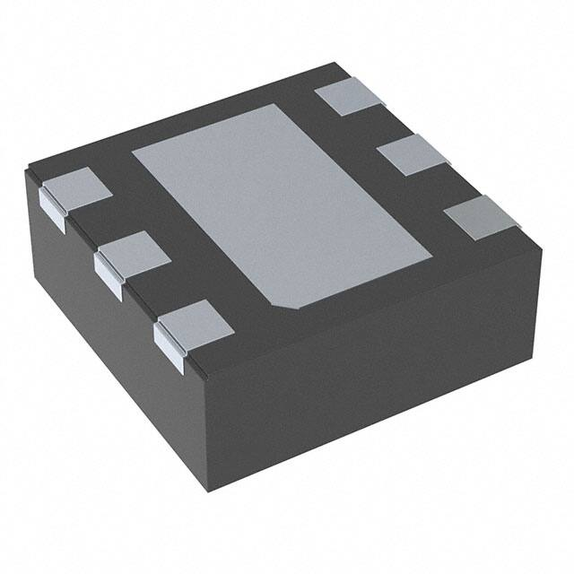
TPS746-Q1 1-A LDO With Power-Good in Small Wettable Flank WSON Packages
1 Features
3 Description
•
The TPS746-Q1 is a 1-A, ultra-low-dropout regulator
(LDO) with power-good functionality. This device is
available in a small 6-pin, 2-mm × 2-mm and a small
8-pin, 3-mm × 3-mm WSON package with wettable
flanks to facilitate optical inspection. The TPS746-Q1
consumes low quiescent current and provides fast line
and load transient performance.
•
•
•
•
•
•
•
•
•
•
•
•
AEC-Q100 qualified for automotive applications:
– Temperature grade 1: –40°C to +125°C, TA
Device operating junction temperature range:
– –40°C to +150°C
Package:
– 2-mm × 2-mm wettable flank WSON
– 3-mm × 3-mm wettable flank WSON
Input voltage range: 1.5 V to 6.0 V
Output voltage range:
– Fixed option: 0.65 V to 5.0 V
– Adjustable option: 0.55 V to 5.5 V
High PSRR: 38 dB at 100 kHz
Output accuracy: ±0.85% typical, ±1.5% maximum
Power-good output options:
– Open-drain or push-pull
Ultra-low dropout:
– 265 mV (max) at 1 A (3.3 VOUT)
Stable with a 1-µF or larger capacitor
Low IQ: 25 µA (typical)
Active output discharge
Low thermal resistance:
– DRV (6-pin WSON), RθJA = 80.3°C/W
– DRB (8-pin WSON), RθJA = 62.0°C/W
2 Applications
•
•
•
•
•
The TPS746-Q1 is a flexible device for post-regulation
by supporting an input voltage range from 1.5 V to
6.0 V and an externally adjustable output range of
0.55 V to 5.5 V. The device also features fixed output
voltages for powering common voltage rails.
The TPS746-Q1 has a power-good (PG) output that
monitors the voltage at the feedback pin to indicate
the status of the output voltage. The EN input and PG
output can be used for sequencing multiple power
supplies in the system.
The TPS746-Q1 is stable with small ceramic output
capacitors, allowing for a small overall solution size. A
precision band-gap and error amplifier provides high
accuracy of ±0.85% (max) at 25°C and ±1.5% (max)
over temperature. This device includes integrated
thermal shutdown, current limit, and undervoltage
lockout (UVLO) features. The TPS746-Q1 has an
internal foldback current limit that helps reduce the
thermal dissipation during short-circuit events.
Automotive head units
Front and rear cameras
Automotive cluster displays
Telematics control units
Medium, short range radar
Device Information (1)
PART NUMBER
TPS746-Q1
(1)
VIN
VOUT
EN
GND
Wettable flank
WSON (6)
2.00 mm × 2.00 mm
Wettable flank
WSON (8)
3.00 mm × 3.00 mm
VIN
VOUT
OUT
IN
Cff
RPG*
TPS746-Q1
CIN
BODY SIZE (NOM)
For all available packages, see the orderable addendum at
the end of the data sheet.
OUT
IN
PACKAGE
COUT
TPS746-Q1
CIN
EN
PG
FB
GND
*Pull-up resistor not required
for push-pull option
PG
COUT
R1
RPG*
R2
*Pull-up resistor not required
for push-pull option
Typical Application: Fixed Voltage Version
Typical Application: Adjustable Voltage Version
An©IMPORTANT
NOTICEIncorporated
at the end of this data sheet addresses availability, warranty, changes, use in
safety-critical
applications,
Copyright
2021 Texas Instruments
Submit
Document
Feedback
intellectual property matters and other important disclaimers. PRODUCTION DATA.
Product Folder Links: TPS746-Q1
1
�TPS746-Q1
www.ti.com
SBVS358B – JUNE 2018 – REVISED JANUARY 2021
Table of Contents
1 Features............................................................................1
2 Applications..................................................................... 1
3 Description.......................................................................1
4 Revision History.............................................................. 2
5 Pin Configuration and Functions...................................3
6 Specifications.................................................................. 5
6.1 Absolute Maximum Ratings ....................................... 5
6.2 ESD Ratings .............................................................. 5
6.3 Recommended Operating Conditions ........................5
6.4 Thermal Information ...................................................6
6.5 Electrical Characteristics ............................................6
6.6 Timing Requirements ................................................. 7
6.7 Typical Characteristics................................................ 8
7 Detailed Description......................................................16
7.1 Overview................................................................... 16
7.2 Functional Block Diagrams....................................... 16
7.3 Feature Description...................................................18
7.4 Device Functional Modes..........................................20
8 Application and Implementation.................................. 21
8.1 Application Information............................................. 21
8.2 Typical Application.................................................... 28
9 Power Supply Recommendations................................29
10 Layout...........................................................................30
10.1 Layout Guidelines................................................... 30
10.2 Layout Examples.................................................... 30
11 Device and Documentation Support..........................31
11.1 Device Support........................................................31
11.2 Documentation Support.......................................... 31
11.3 Receiving Notification of Documentation Updates.. 31
11.4 Support Resources................................................. 31
11.5 Trademarks............................................................. 31
11.6 Electrostatic Discharge Caution.............................. 31
11.7 Glossary.................................................................. 31
4 Revision History
NOTE: Page numbers for previous revisions may differ from page numbers in the current version.
Changes from Revision A (October 2019) to Revision B (January 2021)
Page
• Changed DRB package from preview to production data...................................................................................1
• Added limits to ISC and tSTR in Electrical Charactertistics table.......................................................................... 5
• Changed VDO and VOL(PG) conditions to correct values in Electrical Charactertistics table............................... 5
Changes from Revision * (June 2019) to Revision A (October 2019)
Page
• Changed document status from APL to production data.................................................................................... 1
2
Submit Document Feedback
Copyright © 2021 Texas Instruments Incorporated
Product Folder Links: TPS746-Q1
�TPS746-Q1
www.ti.com
SBVS358B – JUNE 2018 – REVISED JANUARY 2021
5 Pin Configuration and Functions
OUT
1
FB
GND
6
IN
OUT
2 Thermal 5
Pad
PG
NC
3
EN
GND
4
Not to scale
1
NC
2
FB
3
GND
4
Thermal
Pad
6
IN
2 Thermal 5
Pad
PG
3
EN
4
Not to scale
Figure 5-1. DRV Package, 6-Pin Adjustable WSON,
Top View
OUT
1
8
IN
7
NC
Figure 5-2. DRV Package, 6-Pin Fixed WSON,
Top View
OUT
1
NC
2
6
PG
NC
3
5
EN
GND
4
Not to scale
Thermal
Pad
8
IN
7
NC
6
PG
5
EN
Not to scale
Figure 5-3. DRB Package, 8-Pin Adjustable WSON,
Top View
Figure 5-4. DRB Package, 8-Pin Fixed WSON,
Top View
Table 5-1. Pin Functions
PIN
DRV
(Fixed)
DRV
(Adjust)
DRB
(Fixed)
DRB
(Adjust)
I/O
DESCRIPTION
EN
4
4
5
5
Input
Enable pin. Drive EN greater than VEN(HI) to turn on the regulator.
Drive EN less than VEN(LO) to put the low-dropout regulator (LDO)
into shutdown mode.
FB
—
2
—
3
—
This pin is used as an input to the control loop error amplifier and
is used to set the output voltage of the LDO.
GND
3
3
4
4
—
Ground pin.
NAME
IN
6
6
8
8
Input
NC
2
—
2, 3, 7
2, 7
—
OUT
1
1
1
1
Input pin. For best transient response and to minimize input
impedance, use the recommended value or larger ceramic
capacitor from IN to ground as listed in the Recommended
Operating Conditions table and the Input and Output Capacitor
Selection section. Place the input capacitor as close to the output
of the device as possible.
No internal connection. Ground this pin for better thermal
performance.
Regulated output voltage pin. A capacitor is required from OUT to
ground for stability. For best transient response, use the nominal
recommended value or larger ceramic capacitor from OUT to
Output
ground; see the Recommended Operating Conditions table and
the Input and Output Capacitor Selection section. Place the
output capacitor as close to the output of the device as possible.
Submit Document Feedback
Copyright © 2021 Texas Instruments Incorporated
Product Folder Links: TPS746-Q1
3
�TPS746-Q1
www.ti.com
SBVS358B – JUNE 2018 – REVISED JANUARY 2021
Table 5-1. Pin Functions (continued)
PIN
NAME
DRV
(Fixed)
PG
5
DRV
(Adjust)
5
Thermal Pad
4
DRB
(Fixed)
6
DRB
(Adjust)
6
I/O
DESCRIPTION
Power-good output. Available in open-drain and push-pull
topologies. A pullup resistor is required for the open-drain
version. For the open-drain version, if the power-good
Output
functionality is not being used, ground this pin or leave floating.
For the push-pull version, if the power-good functionality is not
being used, leave this pin floating.
—
The thermal pad is electrically connected to the GND node.
Connect to the GND plane for improved thermal performance.
Submit Document Feedback
Copyright © 2021 Texas Instruments Incorporated
Product Folder Links: TPS746-Q1
�TPS746-Q1
www.ti.com
SBVS358B – JUNE 2018 – REVISED JANUARY 2021
6 Specifications
6.1 Absolute Maximum Ratings
over operating free-air temperature range (unless otherwise noted)(1)
MIN
Voltage
(2)
–0.3
6.5
–0.3
6.5
Feedback, VFB
–0.3
2.0
Power-good, VPG
–0.3
6.5
Output, VOUT
–0.3
VIN + 0.3(2)
UNIT
V
Internally limited
Power-good, IPG
Temperature
(1)
Supply, VIN
Enable, VEN
Output, IOUT
Current
MAX
±10
Operating junction, TJ
–40
150
Storage, Tstg
–65
150
mA
°C
Stresses beyond those listed under Absolute Maximum Ratings may cause permanent damage to the device. These are stress ratings
only, which do not imply functional operation of the device at these or any other conditions beyond those indicated under
Recommended Operating Conditions. Exposure to absolute-maximum-rated conditions for extended periods may affect device
reliability.
The absolute maximum rating is VIN + 0.3 V or 6.0 V, whichever is smaller.
6.2 ESD Ratings
VALUE
V(ESD)
(1)
Electrostatic
discharge
Human-body model (HBM), per AEC Q100-002(1)
±2000
Charged-device model (CDM), per AEC Q100-011, corner
pins
±750
Charged-device model (CDM), per AEC Q100-011, other pins
±500
UNIT
V
AEC Q100-002 indicates that HBM stressing shall be in accordance with the ANSI/ESDA/JEDEC JS-001 specification.
6.3 Recommended Operating Conditions
over operating free-air temperature range (unless otherwise noted)
MIN
VIN
Input voltage
VOUT
Output voltage
Adjustable version
0.55
5.5
Fixed version
0.65
5.0
1
IOUT
Output current
0
Input capacitor
1
COUT
Output capacitor(1)
1
CFF
Feed-forward capacitor
Enable voltage
fEN
Enable toggle frequency
VPG
PG voltage
TJ
Junction temperature
(1)
MAX
6.0
CIN
VEN
NOM
1.5
V
V
A
µF
220
10
0
UNIT
µF
nF
6.0
V
10
kHz
0
6.0
V
–40
150
°C
Minimum derated capacitance of 0.47 µF is required for stability.
Submit Document Feedback
Copyright © 2021 Texas Instruments Incorporated
Product Folder Links: TPS746-Q1
5
�TPS746-Q1
www.ti.com
SBVS358B – JUNE 2018 – REVISED JANUARY 2021
6.4 Thermal Information
TPS746-Q1
THERMAL
METRIC(1)
DRV (WSON)
DRB (WSON)
6 PINS
8 PINS
UNIT
RθJA
Junction-to-ambient thermal resistance
80.3
62.0
°C/W
RθJC(top)
Junction-to-case (top) thermal resistance
98.7
73.1
°C/W
RθJB
Junction-to-board thermal resistance
44.8
35.1
°C/W
ψJT
Junction-to-top characterization parameter
6.1
6.3
°C/W
ψJB
Junction-to-board characterization parameter
45.0
35.1
°C/W
RθJC(bot)
Junction-to-case (bottom) thermal resistance
20.8
18.2
°C/W
(1)
For more information about traditional and new thermal metrics, see the Semiconductor and IC Package Thermal Metrics application
report.
6.5 Electrical Characteristics
at operating temperature range (TJ = –40°C to +150°C), VIN = VOUT(NOM) + 0.5 V or 1.5 V (whichever is greater), IOUT = 1 mA,
VEN = VIN, and CIN = COUT = 1 µF (unless otherwise noted); all typical values at TJ = 25°C
PARAMETER
VFB
Output accuracy(1)
MIN
–0.85%
0.85%
–1.00%
1.00%
-40°C ≤ TJ ≤ 150°C
–1.50%
VOUT(NOM) + 0.5 V(2) ≤ VI N ≤ 6.0 V
Load regulation
0.1 mA ≤ IOUT ≤ 1 A, VIN ≥ 2.0 V
V/A
-40°C ≤ TJ ≤ 150°C
25
36
-40°C ≤ TJ ≤ 125°C
0.1
1
-40°C ≤ TJ ≤ 150°C
0.1
1.55
0.01
0.1
µA
1.22
1.5
1.83
A
500
680
850
mA
0.65 V ≤ VOUT < 0.8 V(3)
895
1090
0.8 V ≤ VOUT < 0.9 V
765
960
0.9 V ≤ VOUT < 1.0 V
700
890
1.0 V ≤ VOUT < 1.2 V
IOUT = 1 A,
1.2 V ≤ VOUT < 1.5 V
VOUT = 0.95 x VOUT(NOM)
1.5 V ≤ VOUT < 1.8 V
600
790
465
625
335
480
1.8 V ≤ VOUT < 2.5 V
265
400
2.5 V ≤ VOUT < 3.3 V
195
310
3.3 V ≤ VOUT ≤ 5.5 V
160
265
VEN ≤ 0.3 V,
1.5 V ≤ VIN ≤ 6.0 V
IFB
Feedback pin current
Adjustable only
VOUT(NOM) < 1 V,
VOUT = VOUT(NOM) - 0.2 V, VIN = 2.0 V
VOUT(NOM) ≥ 1 V,
VOUT = VOUT(NOM) × 0.85, VIN = VOUT(NOM) + 1.0 V
Short-circuit current limit VOUT = 0 V
Power-supply rejection
ratio
0.030
mV
32
Shutdown current
PSRR
7.5
25
ISHDN
Dropout voltage
1.50%
2
TJ = 25°C
IOUT = 0 mA
VDO
UNIT
V
-40°C ≤ TJ ≤ 85°C
Ground current
ISC
MAX
TJ = 25°C
Line regulation
Output current limit
TYP
0.55
IGND
ICL
6
TEST CONDITIONS
Feedback voltage
VOUT = 1.8 V,
VIN = 2.8 V,
IOUT = 1 A,
COUT = 2.2 µF
VOUT(NOM) < 1 V,
VIN = 2.0 V
VOUT(NOM) ≥ 1 V,
VIN = VOUT(NOM) + 1.0 V
f = 1 kHz
53
f = 100 kHz
38
f = 1 MHz
30
Submit Document Feedback
µA
µA
mV
dB
Copyright © 2021 Texas Instruments Incorporated
Product Folder Links: TPS746-Q1
�TPS746-Q1
www.ti.com
SBVS358B – JUNE 2018 – REVISED JANUARY 2021
6.5 Electrical Characteristics (continued)
at operating temperature range (TJ = –40°C to +150°C), VIN = VOUT(NOM) + 0.5 V or 1.5 V (whichever is greater), IOUT = 1 mA,
VEN = VIN, and CIN = COUT = 1 µF (unless otherwise noted); all typical values at TJ = 25°C
PARAMETER
TEST CONDITIONS
VN
Output noise voltage
VUVLO
Undervoltage lockout
VUVLO,HYST
Undervoltage lockout
hysteresis
VIN hysteresis
tSTR
Startup time
From EN low-to-high transition to VOUT =
VOUT(NOM) x 95%
VHI
EN pin high voltage
(enabled)
VLO
EN pin low voltage
(disabled)
IEN
Enable pin current
VIN = VEN = 6.0 V
MIN
TYP
BW = 10 Hz to 100 kHz, VOUT = 0.9 V, VIN = 1.9 V
MAX
53
VIN rising
1.21
1.33
1.47
VIN falling
1.17
1.29
1.42
40
200
UNIT
µVRMS
V
mV
500
650
µs
1.0
V
0.3
V
10
nA
RPULLDOWN
Pulldown resistance
VIN = 6.0 V
PGHTH
PG high threshold
VOUT increasing
89
92
95
96
Ω
PGLTH
PG low threshold
VOUT decreasing
86
90
93
PGHYST
PG hysteresis
VOL(PG)
PG pin low-level output
voltage
VOH(PG)
PG pin high-level output
voltage(4)
Ilkg(PG)
PG pin leakage current(5) VOUT > PGHTH, VPG = 6.0 V
TSD
Thermal shutdown
2
%VOUT
%VOUT
%VOUT
VIN ≥ 1.5 V, ISINK = 1 mA
300
VIN ≥ 2.75 V, ISINK = 2 mA
mV
VOUT ≥ 1.0 V, ISOURCE = 0.04 mA
VOUT ≥ 1.4 V, ISOURCE = 0.2 mA
0.8 × VOUT
VOUT ≥ 2.5 V, ISOURCE = 0.5 mA
V
VOUT ≥ 4.5 V, ISOURCE = 1.0 mA
(1)
(2)
(3)
(4)
(5)
7
Shutdown, temperature increasing
170
Reset, temperature decreasing
155
50
nA
°C
When the device is connected to external feedback resistors at the FB pin, external resistor tolerances are not included.
VIN = 1.5V for VOUT < 1.0 V
Dropout is not tested for nominal output voltages below 0.65 V since the input voltage may be below UVLO.
Push-pull version only. The push-pull option is supported only for VOUT ≥ 1.0 V.
Open-drain version only.
6.6 Timing Requirements
PARAMETER
MIN
NOM
MAX
UNIT
tPGDH
PG delay time rising, time from 92% VOUT to
20% of PG(1)
'B' version(2)
135
165
178
µs
4.5
5
5.5
ms
tPGDL
PG delay time falling, time from 90% VOUT to 80% of PG(1)
1.5
7
10
µs
(1)
(2)
Output overdrive = 10%.
See the Device Nomenclature table for more information on available PG timings.
Submit Document Feedback
Copyright © 2021 Texas Instruments Incorporated
Product Folder Links: TPS746-Q1
7
�TPS746-Q1
www.ti.com
SBVS358B – JUNE 2018 – REVISED JANUARY 2021
6.7 Typical Characteristics
0.6
0.6
0.45
0.45
Output Voltage Accuracy (%)
Output Voltage Accuracy (%)
at operating temperature range TJ = 25°C, VIN = VOUT(NOM) + 0.5 V or 1.5 V (whichever is greater), IOUT = 1 mA, VEN = VIN,
and CIN = COUT = 1 μF (unless otherwise noted)
0.3
0.15
0
-0.15
-0.3
-0.45
±
±
-0.6
3.8
4
4.2
TJ
± qC
0qC
qC
qC
4.4
4.6
4.8
5
25qC
85qC
5.2
5.4
125qC
150qC
5.6
5.8
0.3
0.15
0
-0.15
-0.3
-0.45
±
±
-0.6
1.5
6
2
2.5
3
Input Voltage (V)
3.5
4
25qC
85qC
4.5
125qC
150qC
5
5.5
6
Input Voltage (V)
VOUT = 3.3 V, IOUT = 1 mA
VOUT = 0.55 V, IOUT = 1 mA
Figure 6-1. 3.3-V Line Regulation vs VIN
Figure 6-2. 0.55-V Line Regulation vs VIN
320
0.3
±
±
280
0.2
Dropout Voltage (mV)
Output Voltage Accuracy (%)
TJ
± qC
0qC
qC
qC
0.1
0
-0.1
TJ
± qC
0qC
-0.2
±
±
-0.3
5.5
qC
qC
25qC
85qC
TJ
± qC
0qC
qC
qC
25qC
85qC
125qC
150qC
240
200
160
120
80
40
125qC
150qC
0
5.6
5.7
5.8
5.9
6
0
0.1
0.2
0.3
Input Voltage (V)
0.4
0.5
0.6
0.7
0.8
0.9
1
0.9
1
Output Current (A)
VOUT = 5.5 V, IOUT = 1 mA
Figure 6-3. 5.5-V Line Regulation vs VIN
Figure 6-4. 3.3-V Dropout Voltage vs IOUT
320
1,280
±
±
qC
qC
25qC
85qC
125qC
150qC
1,120
1,040
960
880
800
720
TJ
± qC
0qC
qC
qC
25qC
85qC
125qC
150qC
240
200
160
120
80
40
640
0
0.1
0.2
0.3
0.4
0.5
0.6
0.7
0.8
Output Current (A)
0.9
1
0
0
0.1
0.2
0.3
0.4
0.5
0.6
0.7
0.8
Output Current (A)
Figure 6-5. 0.55-V Dropout Voltage vs IOUT
8
±
±
280
Dropout Voltage (mV)
Dropout Voltage (mV)
1,200
TJ
± qC
0qC
Figure 6-6. 5.5-V Dropout Voltage vs IOUT
Submit Document Feedback
Copyright © 2021 Texas Instruments Incorporated
Product Folder Links: TPS746-Q1
�TPS746-Q1
www.ti.com
SBVS358B – JUNE 2018 – REVISED JANUARY 2021
6.7 Typical Characteristics (continued)
at operating temperature range TJ = 25°C, VIN = VOUT(NOM) + 0.5 V or 1.5 V (whichever is greater), IOUT = 1 mA, VEN = VIN,
and CIN = COUT = 1 μF (unless otherwise noted)
1,200
1,100
±
±
Dropout Voltage (mV)
900
TJ
± qC
0qC
qC
qC
25qC
85qC
125qC
150qC
1,050
Ground Pin Current (PA)
1,000
800
700
600
500
400
300
200
900
750
600
450
300
150
100
0
0.5
±
±
qC
qC
TJ
± qC
0qC
25qC
85qC
0.5
0.7
125qC
150qC
0
1
1.5
2
2.5
3
3.5
4
4.5
5
0
0.1
0.2
0.3
Output Voltage (V)
0.4
0.6
0.8
0.9
1
Output Current (A)
IOUT = 1 A
Figure 6-7. VDO vs VOUT
Figure 6-8. IGND vs IOUT
560
2,100
Shutdown Current (nA)
qC
qC
25qC
85qC
125qC
150qC
±
±
480
Ground Pin Current (PA)
±
±
1,800
TJ
± qC
0qC
1,500
1,200
900
600
300
0
25qC
85qC
125qC
150qC
400
320
240
160
80
0
-300
0
0.6
1.2
1.8
2.4
3
3.6
4.2
4.8
5.4
-80
6
0
Input Voltage (V)
0.6
1.2
1.8
2.4
3
3.6
4.2
4.8
5.4
6
Input Voltage (V)
VEN = 0 V
VOUT = 3.3 V, IOUT = 0 mA
Figure 6-9. ISHDN vs VIN
Figure 6-10. IGND vs VIN
1.6
0.8
±
±
1.2
TJ
± qC
0qC
qC
qC
25qC
85qC
125qC
150qC
±
±
0.6
0.8
Change in VOUT (%)
Change in VOUT (%)
TJ
± qC
0qC
qC
qC
0.4
0
-0.4
-0.8
-1.2
qC
qC
TJ
± qC
0qC
25qC
85qC
0.5
0.7
125qC
150qC
0.4
0.2
0
-0.2
-0.4
-0.6
-1.6
-0.8
0
0.1
0.2
0.3
0.4
0.5
0.6
0.7
0.8
0.9
1
0
0.1
Output Current (A)
0.2
0.3
0.4
0.6
0.8
0.9
1
Output Current (A)
VIN = 3.8 V, VOUT = 3.3 V
VIN = 2 V, VOUT = 0.55 V
Figure 6-11. 3.3-V Load Regulation vs IOUT
Figure 6-12. 0.55-V Load Regulation vs IOUT
Submit Document Feedback
Copyright © 2021 Texas Instruments Incorporated
Product Folder Links: TPS746-Q1
9
�TPS746-Q1
www.ti.com
SBVS358B – JUNE 2018 – REVISED JANUARY 2021
6.7 Typical Characteristics (continued)
at operating temperature range TJ = 25°C, VIN = VOUT(NOM) + 0.5 V or 1.5 V (whichever is greater), IOUT = 1 mA, VEN = VIN,
and CIN = COUT = 1 μF (unless otherwise noted)
1.2
640
±
±
qC
qC
25qC
85qC
125qC
150qC
±
±
560
0.6
Output Voltage (mV)
Change in VOUT (%)
0.9
TJ
± qC
0qC
0.3
0
-0.3
-0.6
TJ
± qC
0qC
qC
qC
25qC
85qC
125qC
150qC
480
400
320
240
160
80
-0.9
0
-1.2
0
0.1
0.2
0.3
0.4
0.5
0.6
0.7
0.8
0.9
0
1
0.5
1
1.5
2
2.5
3
3.5
4
4.5
5
Pulldown Current (mA)
Output Current (A)
VIN = 6 V, VOUT = 5 V
Figure 6-14. VOUT vs IOUT Pulldown Resistor
92.5
92.25
92
91.75
91.5
91.25
91
90.75
90.5
90.25
90
89.75
89.5
89.25
89
-50
40
35
PG Leakage Current (nA)
PG Pin Thresholds (%)
Figure 6-13. 5-V Load Regulation vs IOUT
PGLTH
-30
-10
10
30
50
70
90
130
20
15
10
5
0
-10
-50
150
Temperature (qC)
PG = 3.3 V
-25
0
25
50
75
PG = 5.5 V
100
125
150
Temperature (qC)
Figure 6-15. PGLTH and PGHTH vs Temperature
Figure 6-16. IIkg(PG) vs Temperature and PG Pin Voltage
300
166
±
±
240
qC
qC
TJ
± qC
0qC
tPGDH
25qC
85qC
125qC
150qC
PG Delay Time Rising (Ps)
270
PG Pin Voltage Low (mV)
25
-5
PGHTH
110
30
210
180
150
120
90
60
164
162
160
158
156
154
152
30
0
0.2
0.4
0.6
0.8
1
1.2
1.4
1.6
1.8
2
150
-50
PG Pin Sink Current (mA)
-25
0
25
50
75
100
125
150
Temperature (qC)
VIN = 3.8 V, VOUT = 3.3 V
Figure 6-17. VOL(PG) vs PG Pin Sink Current
10
Submit Document Feedback
Figure 6-18. tPGDH vs Temperature
Copyright © 2021 Texas Instruments Incorporated
Product Folder Links: TPS746-Q1
�TPS746-Q1
www.ti.com
SBVS358B – JUNE 2018 – REVISED JANUARY 2021
6.7 Typical Characteristics (continued)
at operating temperature range TJ = 25°C, VIN = VOUT(NOM) + 0.5 V or 1.5 V (whichever is greater), IOUT = 1 mA, VEN = VIN,
and CIN = COUT = 1 μF (unless otherwise noted)
6.5
4.96
tPGDH
PG Delay Time Falling (Ps)
PG Delay Time Rising (ms)
4.92
4.9
4.88
4.86
4.84
4.82
4.8
-50
tPGDL
6.1
4.94
5.7
5.3
4.9
4.5
4.1
3.7
3.3
2.9
-25
0
25
50
75
100
125
2.5
-50
150
Temperature (qC)
-25
50
75
100
125
150
Figure 6-20. tPGDL vs Temperature
300
840
VEN(LO)
800
VEN(HI)
±
±
250
760
Enable Pin Current (PA)
Enable Threshold (mV)
25
Temperature (qC)
Figure 6-19. tPGDH vs Temperature (For TPS746B Only)
720
680
640
600
560
520
TJ
± qC
0qC
qC
qC
125qC
85qC
125qC
150qC
200
150
100
50
0
480
440
-50
0
-50
-25
0
25
50
75
100
125
150
0
0.5
1
1.5
Temperature (qC)
2
2.5
3
3.5
4
4.5
5
5.5
Input Voltage (V)
VEN = 5.5 V
Figure 6-21. VEN(HI) and VEN(LO) vs Temperature
5
4.5
-50qC
-40qC
25qC
85qC
1
1.4
125qC
Input Voltage (V)
Output Voltage (V)
4
TJ
-20qC
0qC
3.5
3
2.5
2
1.5
1
0.5
14
13
12
11
10
9
8
7
6
5
4
3
2
1
0
0
0
0
0.2
0.4
0.6
0.8
1.2
1.6
1.8
Output Current (A)
2
0.5
1
Time (ms)
1.5
25
Vin
20
Vout 15
10
5
0
-5
-10
-15
-20
-25
-30
-35
-40
-45
2
AC-coupled Output Voltage (mV)
Figure 6-22. IEN vs VIN
VOUT = 0.55 V, IOUT = 1 mA, VIN slew rate = 1 V/µs
Figure 6-23. 3.3-V Foldback Current Limit vs IOUT
Figure 6-24. 0.55-V Line Transient
Submit Document Feedback
Copyright © 2021 Texas Instruments Incorporated
Product Folder Links: TPS746-Q1
11
�TPS746-Q1
www.ti.com
SBVS358B – JUNE 2018 – REVISED JANUARY 2021
6.7 Typical Characteristics (continued)
0.2
0.4
0.6
0.8
1
1.2
Time (ms)
1.4
1.6
3.5
3
2
1
-150
0.5
-200
0
-250
-0.5
-300
500
0
240
4.5
160
4
3
0
2.5
-80
2
-160
1.5
-240
1
-320
0.5
-400
0
-480
-0.5
-560
500
200 250 300
Time (us)
350
400
50
100
150
200 250 300
Time (us)
350
400
450
450
240
Iout
Vout
160
3.5
Output Current (A)
80
AC-coupled Output Voltage (mV)
Output Current (A)
3.5
150
-100
Figure 6-26. 1-mA to 1-A Load Transient (0.55 V)
Iout
Vout
100
-50
1.5
Figure 6-25. 3.3-V Line Transient
50
0
VOUT = 0.55 V, VIN = 2 V, IOUT slew rate = 1 A/µs
4.5
0
50
2.5
VOUT = 3.3 V, IOUT = 1 mA, VIN slew rate = 1 V/µs
4
200
Iout
Vout 150
100
4
AC-coupled Output Voltage (mV)
4.5
80
3
0
2.5
-80
2
-160
1.5
-240
1
-320
0.5
-400
0
-480
-0.5
-560
600
0
VOUT = 5 V, VIN = 5.5 V, IOUT slew rate = 1 A/µs
60
120
180
240 300 360
Time (us)
420
480
540
AC-coupled Output Voltage (mV)
0
120
Vin
100
Vout 80
60
40
20
0
-20
-40
-60
-80
-100
-120
-140
-160
1.8
2
Output Current (A)
10
9.5
9
8.5
8
7.5
7
6.5
6
5.5
5
4.5
4
3.5
3
AC-coupled Output Voltage (mV)
Input Voltage (V)
at operating temperature range TJ = 25°C, VIN = VOUT(NOM) + 0.5 V or 1.5 V (whichever is greater), IOUT = 1 mA, VEN = VIN,
and CIN = COUT = 1 μF (unless otherwise noted)
VOUT = 3.3 V, VIN = 3.8 V, IOUT slew rate = 1 A/µs
Figure 6-27. 1-mA to 1-A Load Transient (5 V)
Figure 6-28. 1-mA to 1-A Load Transient (3.3 V)
5
5
4.5
4
4
3.5
3
Voltage (V)
Voltage (V)
3
2.5
2
1.5
1
2
1
0.5
0
Vout
Vin
-0.5
-1
0
200
400
600
Time (us)
VIN = 3.8 V, VOUT = 3.3 V, IOUT = 1 mA
800
1,000
Vout
Venable
Vin
0
-1
0
200
800
1,000
VIN = 3.8 V, VOUT = 3.3 V, IOUT = 1 mA
Figure 6-29. VIN Power-Up
12
400
600
Time (us)
Figure 6-30. Startup With EN
Submit Document Feedback
Copyright © 2021 Texas Instruments Incorporated
Product Folder Links: TPS746-Q1
�TPS746-Q1
www.ti.com
SBVS358B – JUNE 2018 – REVISED JANUARY 2021
6.7 Typical Characteristics (continued)
at operating temperature range TJ = 25°C, VIN = VOUT(NOM) + 0.5 V or 1.5 V (whichever is greater), IOUT = 1 mA, VEN = VIN,
and CIN = COUT = 1 μF (unless otherwise noted)
90
VIN = 3.5 V
VIN = 3.6 V
VIN = 3.7 V
VIN = 3.8 V
80
70
Power-Supply Rejection Ratio (dB)
Power-Supply Rejection Ratio (dB)
90
60
50
40
30
20
10
0
10
100
1k
10k
100k
Frequency (Hz)
1M
80
70
60
50
40
30
VIN = 3.9 V
VIN = 4.0 V
VIN = 4.1 V
VIN = 4.2 V
VIN = 4.3 V
20
10
0
10
10M
VOUT = 3.3 V, IOUT = 500 mA, COUT = 2.2 µF
10k
100k
Frequency (Hz)
1M
10M
Figure 6-32. PSRR vs Frequency and VIN
90
VIN = 3.5 V
VIN = 3.6 V
VIN = 3.7 V
VIN = 3.8 V
80
70
60
50
40
30
20
10
0
10
100
1k
10k
100k
Frequency (Hz)
1M
Power-Supply Rejection Ratio (dB)
90
Power-Supply Rejection Ratio (dB)
1k
VOUT = 3.3 V, IOUT = 500 mA, COUT = 2.2 µF
Figure 6-31. PSRR vs Frequency and VIN
80
70
60
50
40
30
VIN = 3.9 V
VIN = 4.0 V
VIN = 4.1 V
VIN = 4.2 V
VIN = 4.3 V
20
10
0
10
10M
VOUT = 3.3 V, IOUT = 250 mA, COUT = 2.2 µF
Figure 6-33. PSRR vs Frequency and VIN
1k
10k
100k
Frequency (Hz)
1M
10M
Figure 6-34. PSRR vs Frequency and VIN
VIN = 1.9 V, VOUT = 0.9 V
VIN = 2.8 V, VOUT = 1.8 V
VIN = 4.3 V, VOUT = 3.3 V
70
60
50
40
30
20
10
100
1k
10k
100k
Frequency (Hz)
1M
10M
Power-Supply Rejection Ratio (dB)
90
80
0
10
100
VOUT = 3.3 V, IOUT = 250 mA, COUT = 2.2 µF
90
Power-Supply Rejection Ratio (dB)
100
D001
VIN = 2.3 V, VOUT = 1.8 V
VIN = 2.8 V, VOUT = 1.8 V
VIN = 3.8 V, VOUT = 3.3 V
VIN = 4.3 V, VOUT = 3.3 V
80
70
60
50
40
30
20
10
0
10
IOUT = 500 mA, COUT = 2.2 µF
100
1k
10k
100k
Frequency (Hz)
1M
10M
IOUT = 1 A, COUT = 2.2 µF
Figure 6-35. PSRR vs Frequency
Figure 6-36. PSRR vs Frequency
Submit Document Feedback
Copyright © 2021 Texas Instruments Incorporated
Product Folder Links: TPS746-Q1
13
�TPS746-Q1
www.ti.com
SBVS358B – JUNE 2018 – REVISED JANUARY 2021
6.7 Typical Characteristics (continued)
at operating temperature range TJ = 25°C, VIN = VOUT(NOM) + 0.5 V or 1.5 V (whichever is greater), IOUT = 1 mA, VEN = VIN,
and CIN = COUT = 1 μF (unless otherwise noted)
90
COUT = 1 PF
COUT = 2.2 PF
COUT = 4.7 PF
COUT = 47 PF
80
70
Power-Supply Rejection Ratio (dB)
Power-Supply Rejection Ratio (dB)
90
60
50
40
30
20
10
0
10
100
1k
10k
100k
Frequency (Hz)
1M
CFF = 0 nF
CFF = 1 nF
CFF = 10 nF
CFF = 100 nF
80
70
60
50
40
30
20
10
0
10
10M
VIN = 3.8 V, VOUT = 3.3 V, IOUT = 500 mA
20
80
10
1M
10M
IOUT= 100mA, 170PVRMS
IOUT= 500mA, 169PVRMS
IOUT= 1A, 160PVRMS
5
70
2
60
Noise (PV/—Hz)
Power-Supply Rejection Ratio (dB)
10k
100k
Frequency (Hz)
Figure 6-38. PSRR vs Frequency and CFF
90
50
40
30
ILOAD = 10 mA
ILOAD = 100 mA
ILOAD = 250 mA
ILOAD = 500 mA
ILOAD = 1 A
20
10
0
-10
10
100
1k
1
0.5
0.2
0.1
0.05
0.02
0.01
10k
100k
Frequency (Hz)
1M
0.005
10
10M
VIN = 3.8 V, VOUT = 3.3 V, COUT = 2.2 µF
100
1k
10k
100k
Frequency (Hz)
1M
10M
VIN = 3.8 V, VOUT = 3.3 V, COUT = 4.7 µF, VRMS BW = 10 Hz to
100 kHz
Figure 6-40. Output Spectral Noise Density vs Frequency and
IOUT
Figure 6-39. PSRR vs Frequency and ILOAD
20
20
IOUT= 10mA, 159PVRMS
IOUT= 100mA, 160PVRMS
IOUT= 500mA, 160PVRMS
10
5
CFF = 0 nF, 160 PVRMS
CFF = 1 nF, 108 PVRMS
CFF = 10 nF, 74 PVRMS
CFF = 100 nF, 44 PVRMS
10
5
2
Noise (PV/—Hz)
2
Noise (PV/—Hz)
1k
VIN = 3.8 V, VOUT = 3.3 V, IOUT = 500 mA
Figure 6-37. PSRR vs Frequency and COUT
14
100
1
0.5
0.2
0.1
1
0.5
0.2
0.1
0.05
0.05
0.02
0.02
0.01
0.01
0.005
10
0.005
10
100
1k
10k
100k
Frequency (Hz)
1M
10M
100
1k
10k
100k
Frequency (Hz)
1M
10M
VIN = 3.8 V, VOUT = 3.3 V, COUT = 2.2 µF, VRMS BW = 10 Hz to
100 kHz
VIN = 3.8 V, VOUT = 3.3 V, IOUT = 500 mA, COUT = 2.2 µF, VRMS
BW = 10 Hz to 100 kHz
Figure 6-41. Output Spectral Noise Density vs Frequency and
IOUT
Figure 6-42. Output Spectral Noise Density vs Frequency and
CFF
Submit Document Feedback
Copyright © 2021 Texas Instruments Incorporated
Product Folder Links: TPS746-Q1
�TPS746-Q1
www.ti.com
SBVS358B – JUNE 2018 – REVISED JANUARY 2021
6.7 Typical Characteristics (continued)
at operating temperature range TJ = 25°C, VIN = VOUT(NOM) + 0.5 V or 1.5 V (whichever is greater), IOUT = 1 mA, VEN = VIN,
and CIN = COUT = 1 μF (unless otherwise noted)
20
20
COUT = 2.2PF, 160 PVRMS
COUT = 4.7PF, 170 PVRMS
COUT = 47PF, 138 PVRMS
10
5
5
2
Noise (PV/—Hz)
2
Noise (PV/—Hz)
VIN=1.9V, VOUT=0.9V, 53PVRMS
VIN=2.8V, VOUT=1.8V, 96PVRMS
VIN=3.8V, VOUT=3.3V, 160PVRMS
10
1
0.5
0.2
0.1
1
0.5
0.2
0.1
0.05
0.05
0.02
0.02
0.01
0.01
0.005
10
0.005
10
100
1k
10k
100k
Frequency (Hz)
1M
10M
VIN = 3.8 V, VOUT = 3.3 V, IOUT = 100 mA, CFF = 0 µF, VRMS BW
= 10 Hz to 100 kHz
Figure 6-43. Output Spectral Noise Density vs Frequency and
COUT
100
1k
10k
100k
Frequency (Hz)
1M
10M
IOUT = 500 mA, COUT = 2.2 µF, VRMS BW = 10 Hz to 100 kHz
Figure 6-44. Output Spectral Noise Density vs Frequency
Submit Document Feedback
Copyright © 2021 Texas Instruments Incorporated
Product Folder Links: TPS746-Q1
15
�TPS746-Q1
www.ti.com
SBVS358B – JUNE 2018 – REVISED JANUARY 2021
7 Detailed Description
7.1 Overview
The TPS746-Q1 is a low-dropout regulator (LDO) that consumes low quiescent current and delivers excellent
line and load transient performance. These characteristics, combined with low noise and good PSRR with low
dropout voltage, make this device ideal for portable consumer applications.
This regulator offers foldback current limit, shutdown, and thermal protection. The operating junction temperature
for this device is –40°C to +150°C.
7.2 Functional Block Diagrams
IN
OUT
Current
Limit
±
+
Thermal
Shutdown
95 Ÿ
FB
UVLO
PG
±
0.90 x VREF
EN
+
Band Gap
GND
Logic
Figure 7-1. Adjustable Version With Open-Drain Power-Good
IN
OUT
Current
Limit
±
+
Thermal
Shutdown
95 Ÿ
FB
UVLO
PG
±
0.90 x VREF
EN
+
Band Gap
GND
Logic
Figure 7-2. Adjustable Version With Push-Pull Power-Good
16
Submit Document Feedback
Copyright © 2021 Texas Instruments Incorporated
Product Folder Links: TPS746-Q1
�TPS746-Q1
www.ti.com
SBVS358B – JUNE 2018 – REVISED JANUARY 2021
IN
OUT
Current
Limit
±
+
Thermal
Shutdown
95 Ÿ
UVLO
PG
±
0.90 x VREF
EN
+
Band Gap
GND
Logic
Figure 7-3. Fixed Voltage Version With Open-Drain Power-Good
IN
OUT
Current
Limit
±
+
Thermal
Shutdown
95 Ÿ
UVLO
PG
±
0.90 x VREF
EN
+
Band Gap
GND
Logic
Figure 7-4. Fixed Voltage Version With Push-Pull Power-Good
Submit Document Feedback
Copyright © 2021 Texas Instruments Incorporated
Product Folder Links: TPS746-Q1
17
�TPS746-Q1
www.ti.com
SBVS358B – JUNE 2018 – REVISED JANUARY 2021
7.3 Feature Description
7.3.1 Undervoltage Lockout (UVLO)
The TPS746-Q1 uses an undervoltage lockout (UVLO) circuit that disables the output until the input voltage is
greater than the rising UVLO voltage (VUVLO). This circuit ensures that the device does not exhibit any
unpredictable behavior when the supply voltage is lower than the operational range of the internal circuitry.
When VIN is less than VUVLO, the output is connected to ground with a pulldown resistor (RPULLDOWN).
7.3.2 Shutdown
The enable pin (EN) is active high. Enable the device by forcing the EN pin to exceed VEN(HI). Turn off the device
by forcing the EN pin to drop below VEN(LO). If shutdown capability is not required, connect EN to IN.
The TPS746-Q1 has an internal pulldown MOSFET that connects an RPULLDOWN resistor to ground when the
device is disabled. The discharge time after disabling depends on the output capacitance (COUT) and the load
resistance (RL) in parallel with the pulldown resistor (RPULLDOWN). Equation 1 calculates the time constant:
τ = ( RPULLDOWN × RL) / (RPULLDOWN + RL)
(1)
7.3.3 Foldback Current Limit
The device has an internal current limit circuit that protects the regulator during transient high-load current faults
or shorting events. The current limit is a hybrid brickwall-foldback scheme. The current limit transitions from a
brickwall scheme to a foldback scheme at the foldback voltage (VFOLDBACK). In a high-load current fault with the
output voltage above VFOLDBACK, the brickwall scheme limits the output current to the current limit (ICL). When
the voltage drops below VFOLDBACK, a foldback current limit activates that scales back the current as the output
voltage approaches GND. When the output is shorted, the device supplies a typical current called the shortcircuit current limit (ISC). ICL and ISC are listed in the Electrical Characteristics table.
For this device, VFOLDBACK = 0.4 × VOUT(NOM).
The output voltage is not regulated when the device is in current limit. When a current limit event occurs, the
device begins to heat up because of the increase in power dissipation. When the device is in brickwall current
limit, the pass transistor dissipates power [(VIN – V OUT) × ICL]. When the device output is shorted and the output
is below VFOLDBACK, the pass transistor dissipates power [(VIN – VOUT) × ISC]. If thermal shutdown is triggered,
the device turns off. After the device cools down, the internal thermal shutdown circuit turns the device back on.
If the output current fault condition continues, the device cycles between current limit and thermal shutdown. For
more information on current limits, see the Know Your Limits application report.
Figure 7-5 shows a diagram of the foldback current limit.
18
Submit Document Feedback
Copyright © 2021 Texas Instruments Incorporated
Product Folder Links: TPS746-Q1
�TPS746-Q1
www.ti.com
SBVS358B – JUNE 2018 – REVISED JANUARY 2021
VOUT
Brickwall
VOUT(NOM)
VFOLDBACK
Foldback
IOUT
0V
0 mA
ISC
IRATED
ICL
Figure 7-5. Foldback Current Limit
7.3.4 Thermal Shutdown
Thermal shutdown protection disables the output when the junction temperature rises to approximately 170°C.
Disabling the device eliminates the power dissipated by the device, allowing the device to cool. When the
junction temperature cools to approximately 155°C, the output circuitry is again enabled. Depending on power
dissipation, thermal resistance, and ambient temperature, the thermal protection circuit may cycle on and off.
This cycling limits regulator dissipation, protecting the LDO from damage as a result of overheating.
Activating the thermal shutdown feature usually indicates excessive power dissipation as a result of the product
of the (VIN – VOUT) voltage and the load current. For reliable operation limit junction temperature to 125°C,
maximum. To estimate the margin of safety in a complete design, increase the ambient temperature until the
thermal protection is triggered; use worst-case loads and signal conditions.
The TPS746-Q1 internal protection circuitry protects against overload conditions but is not intended to be
activated in normal operation. Continuously running the TPS746-Q1 into thermal shutdown degrades device
reliability.
Submit Document Feedback
Copyright © 2021 Texas Instruments Incorporated
Product Folder Links: TPS746-Q1
19
�TPS746-Q1
www.ti.com
SBVS358B – JUNE 2018 – REVISED JANUARY 2021
7.4 Device Functional Modes
7.4.1 Device Functional Mode Comparison
The Device Functional Mode Comparison table shows the conditions that lead to the different modes of
operation. See the Electrical Characteristics table for parameter values.
Table 7-1. Device Functional Mode Comparison
PARAMETER
OPERATING MODE
VIN
VEN
IOUT
TJ
Normal operation
VIN > VOUT(nom) + VDO and VIN > VIN(min)
VEN > VEN(HI)
IOUT < IOUT(max)
TJ < TSD(shutdown)
Dropout operation
VIN(min) < VIN < VOUT(nom) + VDO
VEN > VEN(HI)
IOUT < IOUT(max)
TJ < TSD(shutdown)
VIN < VUVLO
VEN < VEN(LOW)
Not applicable
TJ > TSD(shutdown)
Disabled
(any true condition
disables the device)
7.4.2 Normal Operation
The device regulates to the nominal output voltage when the following conditions are met:
•
•
•
The input voltage is greater than the nominal output voltage plus the dropout voltage (VOUT(nom) + VDO)
The output current is less than the current limit (IOUT < ICL)
The device junction temperature is less than the thermal shutdown temperature (TJ < TSD)
•
The enable voltage has previously exceeded the enable rising threshold voltage and has not yet decreased
to less than the enable falling threshold
7.4.3 Dropout Operation
If the input voltage is lower than the nominal output voltage plus the specified dropout voltage, but all other
conditions are met for normal operation, the device operates in dropout mode. In this mode, the output voltage
tracks the input voltage. During this mode, the transient performance of the device becomes significantly
degraded because the pass transistor is in the ohmic or triode region, and acts as a switch. Line or load
transients in dropout can result in large output-voltage deviations.
When the device is in a steady dropout state (defined as when the device is in dropout, VIN < VOUT(NOM) + VDO,
directly after being in a normal regulation state, but not during startup), the pass transistor is driven into the
ohmic or triode region. When the input voltage returns to a value greater than or equal to the nominal output
voltage plus the dropout voltage (VOUT(NOM) + VDO), the output voltage can overshoot for a short period of time
while the device pulls the pass transistor back into the linear region.
7.4.4 Disabled
The output of the device can be shutdown by forcing the voltage of the enable pin to less than the maximum EN
pin low-level input voltage (see the Electrical Characteristics table). When disabled, the pass transistor is turned
off, internal circuits are shutdown, and the output voltage is actively discharged to ground by an internal
discharge circuit from the output to ground.
20
Submit Document Feedback
Copyright © 2021 Texas Instruments Incorporated
Product Folder Links: TPS746-Q1
�TPS746-Q1
www.ti.com
SBVS358B – JUNE 2018 – REVISED JANUARY 2021
8 Application and Implementation
Note
Information in the following applications sections is not part of the TI component specification, and TI
does not warrant its accuracy or completeness. TI’s customers are responsible for determining
suitability of components for their purposes, as well as validating and testing their design
implementation to confirm system functionality.
8.1 Application Information
8.1.1 Adjustable Device Feedback Resistors
Figure 8-1 shows that the output voltage of the TPS746P-Q1 can be adjusted from 0.55 V to 5.5 V by using a
resistor divider network.
VIN
VOUT
OUT
IN
Cff
TPS746-Q1
CIN
EN
FB
GND
PG
COUT
R1
RPG*
R2
*Pull-up resistor not required
for push-pull option
Figure 8-1. Adjustable Operation
The adjustable-version device requires external feedback divider resistors to set the output voltage. VOUT is set
using the feedback divider resistors, R1 and R2, according to the following equation:
VOUT = VFB × (1 + R1 / R2)
(2)
To ignore the FB pin current error term in the VOUT equation, set the feedback divider current to 100x the FB pin
current listed in the Electrical Characteristics table. This setting provides the maximum feedback divider series
resistance, as shown in the following equation:
R1 + R2 ≤ VOUT / (IFB × 100)
(3)
8.1.2 Input and Output Capacitor Selection
The TPS746-Q1 requires an output capacitance of 0.47 µF or larger for stability. Use X5R- and X7R-type
ceramic capacitors because these capacitors have minimal variation in value and equivalent series resistance
(ESR) over temperature. When choosing a capacitor for a specific application, pay attention to the dc bias
characteristics for the capacitor. Higher output voltages cause a significant derating of the capacitor. For best
performance, the maximum recommended output capacitance is 220 µF.
Although an input capacitor is not required for stability, good analog design practice is to connect a capacitor
from IN to GND. Some input supplies have a high impedance, thus placing the input capacitor on the input
supply helps reduce the input impedance. This capacitor counteracts reactive input sources and improves
transient response, input ripple, and PSRR. If the input supply has a high impedance over a large range of
frequencies, several input capacitors can be used in parallel to lower the impedance over frequency. Use a
higher-value capacitor if large, fast, rise-time load transients are anticipated, or if the device is located several
inches from the input power source.
Submit Document Feedback
Copyright © 2021 Texas Instruments Incorporated
Product Folder Links: TPS746-Q1
21
�TPS746-Q1
www.ti.com
SBVS358B – JUNE 2018 – REVISED JANUARY 2021
8.1.3 Dropout Voltage
The TPS746-Q1 uses a PMOS pass transistor to achieve low dropout. When (VIN – VOUT) is less than the
dropout voltage (VDO), the PMOS pass device is in the linear region of operation and the input-to-output
resistance is the RDS(ON) of the PMOS pass element. VDO scales approximately with output current because the
PMOS device behaves like a resistor in dropout mode. As with any linear regulator, PSRR and transient
response degrade as (VIN – VOUT) approaches dropout operation.
8.1.4 Exiting Dropout
Some applications have transients that place the LDO into dropout, such as slower ramps on VIN during start-up.
As with other LDOs, the output may overshoot on recovery from these conditions. A ramping input supply
causes an LDO to overshoot on start-up, as shown in Figure 8-2, when the slew rate and voltage levels are in
the correct range. Use an enable signal to avoid this condition.
Input Voltage
Response time for
LDO to get back into
regulation.
Load current discharges
output voltage.
VIN = VOUT(nom) + VDO
Voltage
Output Voltage
Dropout
VOUT = VIN - VDO
Output Voltage in
normal regulation.
Time
Figure 8-2. Startup Into Dropout
Line transients out of dropout can also cause overshoot on the output of the regulator. These overshoots are
caused by the error amplifier having to drive the gate capacitance of the pass element and bring the gate back to
the correct voltage for proper regulation. Figure 8-3 illustrates what is happening internally with the gate voltage
and how overshoot can be caused during operation. When the LDO is placed in dropout, the gate voltage (VGS)
is pulled all the way down to ground to give the pass device the lowest on-resistance as possible. However, if a
line transient occurs when the device is in dropout, the loop is not in regulation and can cause the output to
overshoot until the loop responds and the output current pulls the output voltage back down into regulation. If
these transients are not acceptable, then continue to add input capacitance in the system until the transient is
slow enough to reduce the overshoot.
22
Submit Document Feedback
Copyright © 2021 Texas Instruments Incorporated
Product Folder Links: TPS746-Q1
�TPS746-Q1
www.ti.com
SBVS358B – JUNE 2018 – REVISED JANUARY 2021
Figure 8-3. Line Transients From Dropout
8.1.5 Reverse Current
As with most LDOs, excessive reverse current can damage this device.
Reverse current flows through the body diode on the pass element instead of the normal conducting channel. At
high magnitudes, this current flow degrades the long-term reliability of the device, as a result of one of the
following conditions:
• Degradation caused by electromigration
• Excessive heat dissipation
• Potential for a latch-up condition
Submit Document Feedback
Copyright © 2021 Texas Instruments Incorporated
Product Folder Links: TPS746-Q1
23
�TPS746-Q1
www.ti.com
SBVS358B – JUNE 2018 – REVISED JANUARY 2021
Conditions where reverse current can occur are outlined in this section, all of which can exceed the absolute
maximum rating of VOUT > VIN + 0.3 V:
• If the device has a large COUT and the input supply collapses with little or no load current
• The output is biased when the input supply is not established
• The output is biased above the input supply
If reverse current flow is expected in the application, external protection must be used to protect the device.
Figure 8-4 shows one approach of protecting the device.
Schottky Diode
IN
CIN
Internal Body Diode
OUT
Device
COUT
GND
Figure 8-4. Example Circuit for Reverse Current Protection Using a Schottky Diode
8.1.6 Power Dissipation (PD)
Circuit reliability requires consideration of the device power dissipation, location of the circuit on the printed
circuit board (PCB), and correct sizing of the thermal plane. The PCB area around the regulator must have few
or no other heat-generating devices that cause added thermal stress.
To first-order approximation, power dissipation in the regulator depends on the input-to-output voltage difference
and load conditions. The following equation calculates power dissipation (PD).
PD = (VIN – VOUT) × IOUT
(4)
Note
Power dissipation can be minimized, and therefore greater efficiency can be achieved, by correct
selection of the system voltage rails. For the lowest power dissipation use the minimum input voltage
required for correct output regulation.
For devices with a thermal pad, the primary heat conduction path for the device package is through the thermal
pad to the PCB. Solder the thermal pad to a copper pad area under the device. This pad area must contain an
array of plated vias that conduct heat to additional copper planes for increased heat dissipation.
The maximum power dissipation determines the maximum allowable ambient temperature (TA) for the device.
According to the following equation, power dissipation and junction temperature are most often related by the
junction-to-ambient thermal resistance (RθJA) of the combined PCB and device package and the temperature of
the ambient air (TA).
TJ = TA + (RθJA × PD)
(5)
Thermal resistance (RθJA) is highly dependent on the heat-spreading capability built into the particular PCB
design, and therefore varies according to the total copper area, copper weight, and location of the planes. The
junction-to-ambient thermal resistance listed in the Thermal Information table is determined by the JEDEC
standard PCB and copper-spreading area, and is used as a relative measure of package thermal performance.
24
Submit Document Feedback
Copyright © 2021 Texas Instruments Incorporated
Product Folder Links: TPS746-Q1
�TPS746-Q1
www.ti.com
SBVS358B – JUNE 2018 – REVISED JANUARY 2021
Figure 8-5 and Figure 8-6 show the functions of RθJA and ψJB versus copper area and thickness. These plots are
generated with a 101.6-mm × 101.6-mm × 1.6-mm PCB of two and four layers. For the four layer board, the
inner planes use 1-oz copper thickness. Outer layers are simulated with both 1-oz and 2-oz copper thickness. A
2 x 1 array of thermal vias of 300-µm drill diameter and 25-µm copper (Cu) plating is located beneath the thermal
pad of the device. The thermal vias connect the top layer, the bottom layer and, in the case of the 4-layer board,
the first inner GND plane. Each of the layers has a copper plane of equal area, as shown in Figure 8-7.
140
2 layer PCB, 1 oz copper
2 layer PCB, 2 oz copper
4 layer PCB, 1 oz copper
4 layer PCB, 2 oz copper
130
Thermal Resistance - RTJA (qC/W)
120
110
100
90
80
70
60
50
40
30
0
10
20
30
40
50
60
Cu Area Per Layer (cm2)
70
80
90
100
thet
Figure 8-5. RθJA versus Cu Area for the WSON (DRV) Package
36
2 layer PCB, 1 oz copper
2 layer PCB, 2 oz copper
4 layer PCB, 1 oz copper
4 layer PCB, 2 oz copper
Thermal Resistance -


 工商网监
湘ICP备2023018690号
工商网监
湘ICP备2023018690号

