Product
Folder
Order
Now
Technical
Documents
Support &
Community
Tools &
Software
TPS75003
SBVS052J – OCTOBER 2004 – REVISED NOVEMBER 2018
TPS75003 Configurable Multirail PMIC
1 Features
3 Description
•
The TPS75003 is a complete power management
solution for FPGA, DSP and other multi-supply
applications. The device has been tested with and
meets all of the Xilinx Spartan-3, Spartan-3E, and
Spartan-3L start-up profile requirements, including
monotonic voltage ramp and minimum voltage-rail
rise time. Independent enables for each output allow
sequencing to minimize demand on the power supply
at start-up. Soft-start on each supply limits inrush
current during start-up. Two integrated buck
controllers allow efficient, cost-effective voltage
conversion for both low and high current supplies
such as core and I/O. A 300-mA LDO is integrated to
provide an auxiliary rail such as VCCAUX on the Xilinx
Spartan-3 FPGA. All three output voltages are
externally configurable for maximum flexibility.
1
•
•
•
•
•
•
•
Two 95% Efficient, 3A Buck Controllers and One
300mA LDO
Tested and Endorsed by Xilinx for Powering the
Spartan™-3, Spartan-3E and Spartan-3L FPGAs
Adjustable (1.2V to 6.5V for Bucks, 1.0V to 6.5V
for LDO) Output Voltages on All Channels
Input Voltage Range: 2.2V to 6.5V
Independent Soft-Start for Each Supply
Independent Enable for Each Supply for Flexible
Sequencing
LDO Stable with 2.2μF Ceramic Output Capacitor
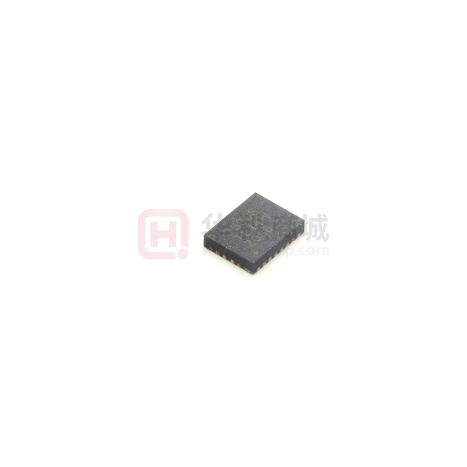
Small, Low-Profile 4.5mm × 3.5mm × 0.9mm
VQFN Package
The TPS75003 is fully specified from –40°C to +85°C
and is offered in a VQFN package, yielding a highly
compact total solution size with high power
dissipation capability.
2 Applications
•
•
•
•
FPGA, DSP, and ASIC Supplies
Set-Top Boxes
DSL Modems
Plasma TV Display Panels
Device Information(1)
PART NUMBER
TPS75003
PACKAGE
VQFN (20)
BODY SIZE (NOM)
4.50 mm × 3.50 mm
(1) For all available packages, see the orderable addendum at
the end of the data sheet.
Typical Application Schematic
TPS75003
IN1
IN2
IN3
EN 1
SS1
EN 2
SS2
EN 3
5V _Input
V CCAUX
IS 1
SW 1
FB 1
IS 2
3A
SW 2
BU CK 2
FB 2
OU T3
300m A
FB 3
LD O
SS3
AG ND
DGND
DGND
3A
BU CK 1
V CCINT
1.2V at 3A
+
DG ND
V CCO
3.3V at 3A
+
V CCAUX
2.5V at 300mA
1
An IMPORTANT NOTICE at the end of this data sheet addresses availability, warranty, changes, use in safety-critical applications,
intellectual property matters and other important disclaimers. PRODUCTION DATA.
�TPS75003
SBVS052J – OCTOBER 2004 – REVISED NOVEMBER 2018
www.ti.com
Table of Contents
1
2
3
4
5
6
7
Features ..................................................................
Applications ...........................................................
Description .............................................................
Revision History.....................................................
Pin Configuration and Functions .........................
Specifications.........................................................
1
1
1
2
3
4
6.1
6.2
6.3
6.4
6.5
6.6
4
4
4
5
5
6
Absolute Maximum Ratings ......................................
ESD Ratings..............................................................
Recommended Operating Conditions.......................
Thermal Information ..................................................
Electrical Characteristics...........................................
Typical Characteristics ..............................................
Detailed Description ............................................ 10
7.1 Overview ................................................................. 10
7.2 Functional Block Diagram ....................................... 11
7.3 Feature Description................................................. 11
8
Application and Implementation ........................ 15
8.1 Application Information............................................ 15
8.2 Typical Application .................................................. 16
9 Power Supply Recommendations...................... 22
10 Layout................................................................... 23
10.1 Layout Guidelines ................................................. 23
10.2 Layout Example .................................................... 24
11 Device and Documentation Support ................. 25
11.1
11.2
11.3
11.4
11.5
11.6
11.7
Device Support......................................................
Documentation Support ........................................
Receiving Notification of Documentation Updates
Community Resources..........................................
Trademarks ...........................................................
Electrostatic Discharge Caution ............................
Glossary ................................................................
25
25
25
25
25
25
25
12 Mechanical, Packaging, and Orderable
Information ........................................................... 26
4 Revision History
NOTE: Page numbers for previous revisions may differ from page numbers in the current version.
Changes from Revision I (August 2010) to Revision J
Page
•
Changed the title of the data sheet and updated the format to the latest TI data sheet format ........................................... 1
•
Moved the ESD rating parameters for HBM and CDM from the Absolute Maximum Ratings table to the ESD Ratings
table ........................................................................................................................................................................................ 4
•
Added the Recommended Operating Conditions table, Overview section, Feature Description section, Design
Requirements section, Power Supply Recommendations section, and Device and Documentation Support section .......... 4
•
Updated the symbols for the thermal resistance parameters in the Thermal Information table............................................. 5
Changes from Revision H (August 2008) to Revision I
•
2
Page
Replaced the Dissipation Ratings table with the Thermal Information table .......................................................................... 5
Submit Documentation Feedback
Copyright © 2004–2018, Texas Instruments Incorporated
Product Folder Links: TPS75003
�TPS75003
www.ti.com
SBVS052J – OCTOBER 2004 – REVISED NOVEMBER 2018
5 Pin Configuration and Functions
IN3
SS3
AGND
EN1
SS1
DGND
SW1
IN1
IS1
19
18
17
16
15
14
13
12
RHL Package
20-Pin VQFN
Top View
20
11
FB1
10
FB2
DGND
6
7
8
DGND
SW2
IN2
9
5
SS2
IS2
4
3
EN3
EN2
2
1
FB3
OUT3
Pin Functions
PIN
TYPE
DESCRIPTION
NAME
NO.
AGND
18
GND
Ground connection for LDO.
DGND
6, 15, PAD
GND
Ground connection for BUCK1 and BUCK2 converters. Pins 6 and 15 should be connected
to the back side exposed pad by a short metal trace as shown in the PCB Layout
Considerations section of this data sheet.
EN1
17
I
Driving the enable pin (ENx) high turns on BUCK1 regulator. Driving this pin low puts it into
shutdown mode, reducing operating current. The enable pin does not trigger on fast negative
going transients.
EN2
4
I
Same as EN1 but for BUCK2 controller.
EN3
3
I
Same as EN1 but for LDO.
FB1
11
I (Analog)
Feedback pin. Used to set the output voltage of BUCK1 regulator.
FB2
10
I (Analog)
Same as FB1 but for BUCK2 controller.
FB3
2
I (Analog)
Same as FB1 but for LDO.
IN1
13
I (Analog)
Input supply to BUCK1.
IN2
8
I (Analog)
Input supply to BUCK2.
IN3
20
I (Power)
Input supply to LDO.
IS1
12
I (Analog)
Current sense input for BUCK1 regulator. The voltage difference between this pin and IN1 is
compared to an internal reference to set current limit. For a robust output start-up ramp,
careful layout and bypassing are required. See the Application Information section for details.
IS2
9
I (Analog)
Same as IS1 but compared to IN2 and used for BUCK2 controller.
OUT3
1
O (Power)
Regulated LDO output. A small ceramic capacitor (≥ 2.2μF) is needed from this pin to ground
to ensure stability.
SS1
16
I (Analog)
Connecting a capacitor between this pin and ground increases start-up time of the BUCK1
regulator by slowing the ramp-up of current limit. This high-impedance pin is noise-sensitive;
careful layout is important. See the Typical Characteristics, Application Information , and
PCB Layout Considerations sections for details.
SS2
5
I (Analog)
Same as SS1 but for BUCK2 regulator.
SS3
19
I (Analog)
Connecting a capacitor from this pin to ground slows the start-up time of the LDO reference,
thereby slowing output voltage ramp-up. See the Application Information section for details.
SW1
14
O (Analog)
Gate drive pin for external BUCK1 P-channel MOSFET.
SW2
7
O (Analog)
Same as SW1 but for BUCK2 controller.
Submit Documentation Feedback
Copyright © 2004–2018, Texas Instruments Incorporated
Product Folder Links: TPS75003
3
�TPS75003
SBVS052J – OCTOBER 2004 – REVISED NOVEMBER 2018
www.ti.com
6 Specifications
6.1 Absolute Maximum Ratings
Over operating free-air temperature range (unless otherwise noted) (1)
MIN
MAX
UNIT
VINX
IN1, IN2, IN3 voltage
–0.3
7
V
VENX
EN1, EN2, EN3 voltage
–0.3
VINX + 0.3
V
VSWX
SW1, SW2, SW3 voltage
–0.3
VINX + 0.3
V
VISX
IS1, IS2, IS3 voltage
–0.3
VINX + 0.3
V
VOUT3
OUT3 voltage
–0.3
7
V
VSSX
SS1, SS2, SS3 voltage
–0.3
VINX + 0.3
V
VFBX
FB1, FB2, FB3 voltage
–0.3
3.3
V
IOUT3
Peak LDO output current
Internally limited
Continuous total power dissipation
See Thermal Information Table
TJ
Junction temperature
–55
150
°C
Tstg
Storage temperature
–65
150
°C
(1)
Stresses beyond those listed under Absolute Maximum Ratings may cause permanent damage to the device. These are stress ratings
only, which do not imply functional operation of the device at these or any other conditions beyond those indicated under Recommended
Operating Conditions. Exposure to absolute-maximum-rated conditions for extended periods may affect device reliability.
6.2 ESD Ratings
VALUE
V(ESD)
(1)
(2)
Electrostatic
discharge
Human-body model (HBM), per ANSI/ESDA/JEDEC JS-001 (1)
1000
Charged-device model (CDM), per JEDEC specification JESD22-C101 (2)
500
UNIT
V
JEDEC document JEP155 states that 500-V HBM allows safe manufacturing with a standard ESD control process.
JEDEC document JEP157 states that 250-V CDM allows safe manufacturing with a standard ESD control process.
6.3 Recommended Operating Conditions
over operating free-air temperature range (unless otherwise noted)
MIN
NOM
MAX
UNIT
VIN1
Input voltage at IN1 pin
2.2
6.5
V
VOUT1
Output voltage of BUCK1
1.2
VIN1
V
IOUT1
Maximum output current of BUCK1
3
A
VIN2
Input voltage at IN2 pin
2.2
6.5
V
VOUT2
Output voltage of BUCK1
1.2
VIN2
V
IOUT2
Maximum output current of BUCK2
3
A
VIN3
Input voltage at IN3 pin
2.2
6.5
V
VOUT3
Output voltage of LDO
1
VIN3 – VDO
V
IOUT3
Maximum output current of LDO
4
300
Submit Documentation Feedback
mA
Copyright © 2004–2018, Texas Instruments Incorporated
Product Folder Links: TPS75003
�TPS75003
www.ti.com
SBVS052J – OCTOBER 2004 – REVISED NOVEMBER 2018
6.4 Thermal Information
TPS75003
THERMAL METRIC (1)
RHL (VQFN)
UNIT
20 PINS
RθJA
Junction-to-ambient thermal resistance
42.6
°C/W
RθJC(top)
Junction-to-case (top) thermal resistance
51.8
°C/W
RθJB
Junction-to-board thermal resistance
39.5
°C/W
ψJT
Junction-to-top characterization parameter
0.6
°C/W
ψJB
Junction-to-board characterization parameter
14.2
°C/W
RθJC(bot)
Junction-to-case (bottom) thermal resistance
2.8
°C/W
(1)
For more information about traditional and new thermal metrics, see the Semiconductor and IC Package Thermal Metrics application
report.
6.5 Electrical Characteristics
VEN1 = VIN1, VEN2 = VIN2, VEN3 = VIN3, VIN1 = VIN2 = 2.2V, VIN3 = 3.0V, VOUT3 = 2.5V, COUT1 = COUT2 = 47μF, COUT3 = 2.2μF, TA =
–40°C to +85°C, unless otherwise noted. Typical values are at TA = +25°C.
PARAMETER
TEST CONDITIONS
MIN
TYP
MAX
UNIT
Supply and Logic
VINX
Input Voltage Range
(IN1, IN2, IN3) (1)
IQ
Quiescent Current, IQ = IDGND +
IAGND
IOUT1 = IOUT2 = 0mA, IOUT3 = 1mA
ISHDN
Shutdown Supply Current
VEN1 = VEN2 = VEN3 = 0V
VIH1, 2
Enable High, enabled
(EN1, EN2)
VIH3
Enable High, enabled (EN3)
VILX
Enable Low, shutdown
(EN1, EN2, EN3)
IENX
Enable pin current
(EN1, EN2, EN3)
2.2
6.5
V
75
150
μA
0.05
3
μA
1.4
VINX
V
1.14
VIN3
V
0
0.3
V
0.5
μA
VINX
V
0.01
Buck Controllers 1 and 2
VOUT1,2
Adjustable Output Voltage
Range (2)
VFB1,2
Feedback Voltage (FB1, FB2)
VFBX
1.220
Feedback Voltage Accuracy (1)
(FB1, FB2)
–2%
V
2%
IFB1,2
Current into FB1, FB2 pins
VIS1,2
Reference Voltage for Current
Sense
IIS1,2
Current into IS1, IS2 Pins
ΔVOUT%/ΔVIN
Line Regulation (1)
Measured with the circuit in
Figure 18,
VOUT + 0.5V ≤ VIN ≤ 6.5V
0.1
%/V
ΔVOUT%/ΔIOU
Load Regulation
Measured with the circuit in
Figure 18,
30mA ≤ I OUT ≤ 2A
0.6
%/A
n1,2
Efficiency (3)
Measured with the circuit in
Figure 18, IOUT = 1A
94%
tSTR1,2
Startup Time (3)
Measured with the circuit in
Figure 18,
RL = 6Ω, COUT = 100μF, CSS = 2.2nF
T
(1)
(2)
(3)
80
0.01
0.5
μA
100
120
mV
0.01
0.5
μA
5
ms
To be in regulation, minimum VIN1 (or VIN2) must be greater than VOUT1,NOM (or VOUT2,NOM) by an amount determined by external
components. Minimum VIN3 = VOUT3 + VDO or 2.2V, whichever is greater.
Maximum VOUT depends on external components and will be less than VIN.
Depends on external components.
Submit Documentation Feedback
Copyright © 2004–2018, Texas Instruments Incorporated
Product Folder Links: TPS75003
5
�TPS75003
SBVS052J – OCTOBER 2004 – REVISED NOVEMBER 2018
www.ti.com
Electrical Characteristics (continued)
VEN1 = VIN1, VEN2 = VIN2, VEN3 = VIN3, VIN1 = VIN2 = 2.2V, VIN3 = 3.0V, VOUT3 = 2.5V, COUT1 = COUT2 = 47μF, COUT3 = 2.2μF, TA =
–40°C to +85°C, unless otherwise noted. Typical values are at TA = +25°C.
PARAMETER
TEST CONDITIONS
MIN
TYP
VIN1,2 > 2.5V
4
VIN1,2 = 2.2V
6
MAX
UNIT
RDS,ON1,2
Gate Driver P-Channel and NChannel MOSFET OnResistance
ISW1,2
Gate Driver P-Channel and NChannel MOSFET Drive Current
tON
Minimum On Time
1.36
1.55
1.84
μs
tOFF
Minimum Off Time
0.44
0.65
0.86
μs
6.5 – VDO
V
Ω
100
mA
LDO
VOUT3
Output Voltage Range
VFB3
Feedback Pin Voltage
1
0.507
Feedback Pin Voltage
Accuracy (1)
2.95V ≤ VIN3 ≤ 6.5V
1mA ≤ IOUT3 ≤ 300mA
ΔVOUT%/ΔVIN
Line Regulation (1)
VOUT3 + 0.5V ≤ VIN3 ≤ 6.5V
ΔVOUT%/ΔIOU
Load Regulation
VDO
V
–4%
4%
0.075
%/V
10mA ≤ IOUT3 ≤ 300mA
0.01
%/mA
Dropout Voltage
(VIN = VOUT(NOM) – 0.1) (4)
IOUT3 = 300mA
250
350
mV
ICL3
Current Limit
VOUT = 0.9 x VOUT(NOM)
600
1000
mA
IFB3
Current into FB3 pin
0.03
0.1
μA
Vn
Output Noise
tSD
Thermal Shutdown Temperature
for LDO
T
UVLO
(4)
375
BW = 100Hz – 100kHz,
IOUT3 = 300mA
400
Shutdown, Temp Increasing
175
Reset, Temp Decreasing
160
μVRMS
°C
Under-Voltage Lockout Threshold VIN Rising
1.80
V
Under-Voltage Lockout
Hysteresis
100
mV
VIN Falling
VDO does not apply when VOUT + VDO < 2.2V.
6.6 Typical Characteristics
Measured using circuit in Figure 18.
6.6.1 Buck Converter
5
5
4
4
TA = -40°C
3
3
2
TA = +85°C
1
TA = +25 °C
0
-1
D VOUT (%)
DV OUT (%)
2
-2
-3
-3
-4
-4
TA = -40°C
-5
0
0.5
VIN = 3.3 V
1.0
1.5
2.0
IOUT (A)
2.5
3.0
VOUT = 1.2 V
3.5
0
0.5
VIN = 5 V
Figure 1. Buck Load Regulation
6
TA = +85°C
0
-1
-2
-5
TA = +25 °C
1
Submit Documentation Feedback
1.0
1.5
2.0
I OUT (A)
2.5
3.0
3.5
VOUT = 3.3 V
Figure 2. Buck Load Regulation
Copyright © 2004–2018, Texas Instruments Incorporated
Product Folder Links: TPS75003
�TPS75003
www.ti.com
SBVS052J – OCTOBER 2004 – REVISED NOVEMBER 2018
Buck Converter (continued)
5
5
4
4
3
TA = +25 °C
TA = +25°C
2
D VOUT (%)
D VOUT (%)
2
3
TA = -40°C
1
0
TA = +85°C
-1
0
-1
-2
-2
-3
-3
-4
-4
-5
TA = +85°C
1
TA = -40 °C
-5
2.0
2.5
3.0
3.5
4.0
4.5
5.0
5.5
6.0
6.5
3.0
7.0
3.5
4.0
4.5
VOUT = 1.2 V
VOUT = 3.3 V
IOUT = 2 A
5.5
6.0
6.5
7.0
IOUT = 2 A
Figure 4. Buck Line Regulation
Figure 3. Buck Line Regulation
600
Switching Frequency (kHz)
500
Switching Frequency (kHz)
5.0
VIN (V)
VIN (V)
400
VIN = 3.3V
300
200
VIN = 5.0V
-40ºC
100
+25ºC
500
VIN = 2.2V
VOUT = 1.2V
400
VIN = 3.3V
VOUT = 1.2V
300
200
100
VIN = 5.0V
VOUT = 1.2V
+85ºC
0
VIN = 5.0V
VOUT = 3.3V
0
0
0.5
1.0
1.5
2.0
2.5
3.0
0.01
0.1
IOUT (A)
1.0
10
IOUT (A)
VOUT = 1.2 V
Figure 5. Buck Switching Frequency vs IOUT, TA
Figure 6. Buck Switching Frequency vs IOUT
100
VIN = 5.0V
VOUT = 3.3V
90
Efficiency (%)
80
70
VIN = 5.0V
VOUT = 1.2V
60
50
40
VIN = 3.3V
30
VOUT = 1.2V
20
10
0
0.0001
0.001
0.01
0.1
1
10
IOUT (A)
Figure 7. Efficiency vs IOUT
Submit Documentation Feedback
Copyright © 2004–2018, Texas Instruments Incorporated
Product Folder Links: TPS75003
7
�TPS75003
SBVS052J – OCTOBER 2004 – REVISED NOVEMBER 2018
www.ti.com
5
5
4
4
3
3
2
2
1
DVOUT (%)
DVOUT (%)
6.6.2 LDO Converter
TA = -40ºC
0
-1
TA = +25ºC
-2
TA = +25ºC
1
0
-1
TA = +85ºC
-2
TA = +85ºC
-3
-3
-4
-4
TA = -40ºC
-5
-5
0
0.05
0.1
0.15
0.2
0.25
0.3
0.35
0.4
3.0
3.5
4.0
4.5
IOUT (A)
VIN = 3.3 V
VOUT = 2.5 V
VOUT = 2.5 V
Figure 8. LDO Load Regulation
5.5
6.0
6.5
7.0
IOUT = 1 mA
Figure 9. LDO Line Regulation
450
500
TA = +25°C
400
400
350
TA = +85°C
300
VDO (mV)
VDO (mV)
5.0
VIN (V)
300
200
TA = -40 °C
250
200
150
100
100
50
0
0
0
50
100
150
200
250
300
350
400
450
-40
-25
-10
VIN = 3.3 V
VOUT = 2.5 V
VOUT = 2.5 V
20
35
50
65
80 85
IOUT = 300 mA
Figure 11. LDO Dropout vs TA
Figure 10. LDO Dropout vs IOUT
12
12
10
10
TA = - 40ºC
TA = +25ºC
8
RDS, ON (W)
8
RDS,ON (W)
5
Ambient Temperature (°C)
I OUT (mA)
6
TA = +25ºC
4
TA = +85ºC
6
4
TA = +85ºC
2
2
0
0
TA = - 40ºC
2.0
8
2.5
3.0
3.5
4.0
4.5
5.0
5.5
6.0
6.5
7.0
2.0
2.5
3.0
3.5
4.0
4.5
5.0
5.5
6.0
VIN (V)
VIN (V)
Figure 12. RDS,ON PMOS vs VIN
Figure 13. RDS,ON NMOS vs VIN
Submit Documentation Feedback
6.5
7.0
Copyright © 2004–2018, Texas Instruments Incorporated
Product Folder Links: TPS75003
�TPS75003
www.ti.com
SBVS052J – OCTOBER 2004 – REVISED NOVEMBER 2018
LDO Converter (continued)
2.525
2.520
2.515
VOUT (V)
2.510
2.505
2.500
2.495
2.490
2.485
2.480
2.475
-40
-15
10
35
60
85
Ambient Temperature (ºC)
VIN = 3.3 V
Figure 14. LDO VOUT vs TA
Submit Documentation Feedback
Copyright © 2004–2018, Texas Instruments Incorporated
Product Folder Links: TPS75003
9
�TPS75003
SBVS052J – OCTOBER 2004 – REVISED NOVEMBER 2018
www.ti.com
7 Detailed Description
7.1 Overview
The TPS75003 device is a power management IC (PMIC) with two buck controllers and one integrated LDO
regulator. The three voltage regulators have independent enable pins for flexible power sequence timing, and all
of the output voltages are set by external feedback resistor dividers. The independent power regulators can be
wired in parallel, in series, or connected to separate input voltages as needed to meet the requirements of the
application.
The two buck controllers are identical and operate over a input voltage range of 2.2 V to 6.5 V to supply a load
with an externally configurable output voltage with up to 3-A of current. The buck controllers drive the gate of a
single PMOS FET in an asynchronous buck regulator architecture. The use of a PMOS FET lets the buck
regulator operate with 100% duty cycle when the input voltage is approximately equal to or less than the desired
output voltage. The buck controllers have an eternally configurable current sense feature to limit the output
current and protect the PMOS FET. The buck controllers have an externally configurable soft-start feature that
ramps the voltage and meet the timing requirements of the load.
The LDO regulator integrates the FET and operates over the same input voltage range of 2.2 V to 6.5 V to
supply a load with an externally configurable output voltage with up to 300-mA of current. The LDO regulator
includes integrated current limiting and thermal protection features. The LDO regulator also has an externally
configurable soft-start feature to ramp the voltage to meet desired timing requirements.
10
Submit Documentation Feedback
Copyright © 2004–2018, Texas Instruments Incorporated
Product Folder Links: TPS75003
�TPS75003
www.ti.com
SBVS052J – OCTOBER 2004 – REVISED NOVEMBER 2018
7.2 Functional Block Diagram
TPS75003
IN1
≤ 3A Buck Controller
IS1
VIS 1
Switch
Control
SW1
Soft
Start
Control
SS1
EN1
VR E F1
FB1
DGND
IN2
≤ 3A Buck Controller
IS2
VIS2
Switch
Control
SW2
Soft
Start
Control
SS2
EN2
VR E F2
FB2
DGND
300mA LDO
IN3
OUT3
Thermal/
Current
Limit
EN3
FB3
VREF 3
SS3
AGND
7.3 Feature Description
7.3.1 Operation (Buck Controllers)
Channels 1 and 2 have two identical non-synchronous buck controllers that use minimum on-time and minimum
off-time hysteretic control (see Figure 18. For clarity, BUCK1 is used throughout the discussion of device
operation. When VOUT1 is less than its target, an external PMOS (Q1) is turned on for at least the minimum ontime, increasing current through the inductor (L1) until VOUT1 reaches its target value or the current limit (set by
R1) is reached. When either of these conditions is met, the PMOS is switched off for at least the minimum offtime of the device. After the minimum off-time has passed, the output voltage is monitored and the switch is
turned on again when necessary.
Submit Documentation Feedback
Copyright © 2004–2018, Texas Instruments Incorporated
Product Folder Links: TPS75003
11
�TPS75003
SBVS052J – OCTOBER 2004 – REVISED NOVEMBER 2018
www.ti.com
Feature Description (continued)
When output current is low, the buck controllers operate in discontinuous mode. In this mode, each switching
cycle begins at zero inductor current, rises to a maximum value, then falls back to zero current. When current
reaches zero on the falling edge, ringing occurs at the resonant frequency of the inductor and stray switch node
capacitance. This operation is normal; it does not affect circuit performance, and can be minimized if desired by
using an RC snubber, a resistor in series with the gate of the PMOS, or both as shown in Figure 15.
Q
L
R
D
0.1mF
f = measured resonant
frequency at switch node
R = 2πfL
Figure 15. RC Snubber and Series Gate Resistor Used to Minimize Ringing
At higher output currents, the TPS75003 device operates in continuous mode. In continuous mode, there is no
ringing at the switch node and VOUT is equal to VIN times the duty cycle of the switching waveform.
When VIN approaches or falls to less than VOUT, the buck controllers operate in 100% duty cycle mode, fully
turning on the external PMOS to let regulation occur at a lower dropout than would otherwise be possible.
7.3.2 Enable (Buck Controllers)
The enable pins (EN1 and EN2) for the buck controllers are active high. When the enable pin is driven low and
input voltage is present at IN1 or IN2, an on-chip FET is turned on to discharge the soft-start pin SS1 or SS2,
respectively. If the soft-start feature is being used, enable should be driven high at least 10μs after VIN is applied
to make sure that this discharge cycle occurs.
7.3.3 UVLO (Buck Controllers)
The device has an undervoltage lockout circuit to prevent the turnon of the external PMOS (Q1 or Q2) until a
reliable operating voltage is reached on the appropriate regulator (IN1 or IN2). This prevents the buck controllers
from misoperation at low input voltages.
7.3.4 Current Limit (Buck Controllers)
An external resistor (R1 or R2) is used to set the current limit for the external PMOS transistor (Q1 or Q2). These
resistors are connected between IN1 and IS1 (or IN2 and IS2) to provide a reference voltage across these pins
that is proportional to the current flowing through the PMOS transistor. This reference voltage is compared to an
internal reference to determine if an overcurrent condition exists. When current limit is exceeded, the external
PMOS is turned off for the minimum off-time. Current limit detection is disabled for 10ns any time the PMOS is
turned on to avoid triggering on switching noise. In 100% duty cycle mode, current limit is always enabled.
Current limit is calculated using the VIS1 or VIS2 specification in the Electrical Characteristics section as shown in
Equation 1.
ILIMIT
VIS1,2
R1,2
(1)
The current limit resistor must be appropriately rated for the dissipated power determined by its RMS current
calculated by Equation 2.
IRMS | IOUT D
PDISS
12
IRMS
2
IOUT
VOUT
VIN
uR
(2)
Submit Documentation Feedback
Copyright © 2004–2018, Texas Instruments Incorporated
Product Folder Links: TPS75003
�TPS75003
www.ti.com
SBVS052J – OCTOBER 2004 – REVISED NOVEMBER 2018
Feature Description (continued)
For low-cost applications the IS1,2 pin can be connected to the drain of the PMOS, using RDS,ON instead of R1 or
R2 to set current limit. Variations in the PMOS RDS,ON must be considered to make sure that current limit will
protect external components such as the inductor, the diode, and the switch itself from damage as a result of
overcurrent.
7.3.5 Short-Circuit Protection (Buck Controllers)
In an overload condition, the current rating of the external components (PMOS, diode, and inductor) can be
exceeded. To help guard against this, the TPS75003 device increases its minimum off-time when the voltage at
the feedback pin is less than the reference voltage. When the output is shorted (VFB is zero), the minimum offtime is increased to approximately 4μs. The increase in off-time is proportional to the difference between the
voltage at the feedback pin and the internal reference.
7.3.6 Soft-Start (Buck Controllers)
The buck controllers each have independent soft-start capability to limit inrush during start-up and to meet timing
requirements of the Xilinx Spartan-3 FPGA. Limiting inrush current by using soft-start, or by staggering the turnon
of power rails, also guards against voltage drops at the input source due to its output impedance. Refer to the
soft-start circuitry shown in Figure 16 and the soft-start timing diagram shown in Figure 17. The BUCK1 controller
is discussed in this section; it is identical to BUCK2. Note that pins SS1 and SS2 are very high-impedance and
cannot be probed using a typical oscilloscope setup. When input voltage is applied at IN1 and EN1 is driven low,
any charge on the SS pin is discharged by an on-chip pulldown transistor. When EN1 is driven high, an on-chip
current source starts charging the external soft-start capacitor CSS1. The voltage on the capacitor is compared to
the voltage across the current sense resistor R1 to determine if an overcurrent condition exists. If the voltage
drop across the sense resistor becomes greater than the reference voltage, then the external PMOS is shut off
for the minimum off-time. This implementation provides a cycle-by-cycle current limit and lets the user configure
the soft-start time over a wide range for most applications. For detailed information on selecting CSS1 and CSS2,
see the Soft-Start Capacitor Selection (Buck Controllers) section.
IN1
IS1
VIN
V IS1
Switch
Control
SS1
SW1
Soft
Start
Control
EN1
Current
Limit
VSS1
Figure 16. Soft-Start Circuitry
VEN1
Time
Figure 17. Soft-Start Timing Diagram
Submit Documentation Feedback
Copyright © 2004–2018, Texas Instruments Incorporated
Product Folder Links: TPS75003
13
�TPS75003
SBVS052J – OCTOBER 2004 – REVISED NOVEMBER 2018
www.ti.com
7.3.7 LDO Operation
The TPS75003 LDO regulator uses a PMOS pass transistor and is offered in an adjustable version to easily
configure any output voltage. When used to power VCC,AUX the LDO regulator output voltage is set to 2.5V; the
LDO regulator can optionally be set to other output voltages to power other circuitry. The LDO regulator has
integrated soft-start, independent enable, and short-circuit and thermal protection. The LDO regulator can be
used to power VCC,AUX on the Xilinx Spartan-3 FPGA when 3.3V JTAG signals are used as described in the
Using 3.3-V Signals for Spartan-3 Configuration and JTAG Ports application note.
7.3.8 Internal Current Limit (LDO)
The internal current limit of the LDO regulator helps protect the regulator during fault conditions. When an
overcurrent condition is detected, the output voltage is decreased until the current falls to a level that will not
damage the device. For good device reliability, the LDO regulator should not operate at the current limit.
7.3.9 Enable Pin (LDO)
The active high enable pin (EN3) can be used to put the device into shutdown mode. If shutdown and soft-start
capability are not required, EN3 can be tied to IN3.
7.3.10 Dropout Voltage (LDO)
The LDO regulator uses a PMOS transistor to achieve low dropout. When (VIN – VOUT) is less than the dropout
voltage (VDO), the pass transistor is in its linear region of operation, and the input-output resistance is the RDS,ON
of the pass transistor. In this region, the LDO regulator is said to be out of regulation; ripple rejection, line
regulation, and load regulation degrade as (VIN – VOUT) decreases to much lower than 0.5V.
7.3.11 Transient Response (LDO)
The LDO regulator does not have an on-chip pulldown circuit for output is overvoltage conditions. This feature
lets the device be used in applications that connect higher voltage sources such as an alternate power supply to
the output. This design also results in an output overshoot of several percent if the load current quickly drops to
zero. The amplitude of overshoot can be reduced by increasing COUT; the duration of overshoot can be
decreased by adding a load resistor.
7.3.12 Thermal Protection (LDO)
Thermal protection disables the output when the junction temperature, TJ, reaches unsafe levels. When the
junction temperature cools, the output is enabled again. The thermal protection circuit may cycle on and off
depending on the power dissipation, thermal resistance, and ambient temperature. This cycling limits the
dissipation of the regulator, protecting it from damage. For good long term reliability, the device should not be
continuously operated at or near thermal shutdown.
7.3.13 Power Dissipation (LDO)
The TPS75003 device is available in a QFN-style package with an exposed lead frame on the package
underside. The exposed lead frame is the primary path for removing heat and should be soldered to a PC board
that is configured to remove the amount of power dissipated by the LDO regulator, as calculated by Equation 3.
PD
VIN3
VOUT3 u IOUT3
(3)
Power dissipation can be minimized by using the lowest possible input voltage necessary to ensure the required
output voltage. The two buck converters do not contribute a significant amount of dissipated power. Using
heavier copper will increase the overall effectiveness of removing heat from the device. The addition of plated
through-holes to heat-dissipating layers will also improve the heatsink effectiveness.
14
Submit Documentation Feedback
Copyright © 2004–2018, Texas Instruments Incorporated
Product Folder Links: TPS75003
�TPS75003
www.ti.com
SBVS052J – OCTOBER 2004 – REVISED NOVEMBER 2018
8 Application and Implementation
NOTE
Information in the following applications sections is not part of the TI component
specification, and TI does not warrant its accuracy or completeness. TI’s customers are
responsible for determining suitability of components for their purposes. Customers should
validate and test their design implementation to confirm system functionality.
8.1 Application Information
The TPS75003 is an integrated power management IC designed specifically to power DSPs and FPGAs such as
the Xilinx Spartan-3, Spartan-3E and Spartan-3L. Two non-synchronous buck controllers can be configured to
supply up to 3A for both CORE and I/O rails. A low dropout linear regulator powers auxiliary rails up to 300mA.
All channels have independent enable and soft-start, allowing control of inrush current and output voltage ramp
time as required by the application.
Table 1 through Table 4 show component values that have been tested for use with up to 3A load currents.
Inductors in Table 1 are tested up to the respective saturation currents. Other similar external components can
be substituted as desired; however, in all cases the circuits that are used should be tested for compliance to
application requirements.
Table 1. Inductors Tested with the TPS75003
PART NUMBER
SLF7032T−100M1R4
SLF6025−150MR88
MANUFACTURER
INDUCTANCE
DC RESISTANCE
SATURATION CURRENT
TDK
10μH ±20%
53mΩ ±20%
1.4A
TDK
15μH ±20%
85mΩ ±20%
0.88A
CDRH6D28−5R0
Sumida
5μH
23mΩ
2.4A
CDRH6D38-5R0
Sumida
5μH
18mΩ
2.9A
CDRH103R−100
Sumida
10μH
45mΩ
2.4A
CDRH4D28−100
Sumida
10μH
96mΩ
1.0A
CDRH8D43-150
Sumida
15μH
42mΩ
2.9A
CDRH5D18−6R2
Sumida
6.2μH
71mΩ
1.4A
DO3316P−472
Coilcraft
4.7μH
18mΩ
5.4A
MSS7341-153
Coilcraft
15μH
55mΩ
1.6A
MSS7341-223
Coilcraft
22μH
82mΩ
1.26A
744052006
Wurth
6.2μH
80mΩ
1.45A
74451115
Wurth
15μH
90mΩ
0.8A
Table 2. PMOS Transistors Tested with the TPS75003
PART NUMBER
MANUFACTURER
RDS,ON (TYP)
VDS
SI5457DC-T1-GE3
Vishay
0.056Ω at VGS = –2.5V
–20V
–6A at +25°C
1206-8
SI2301BDS-T1-E3
Vishay
0.15Ω at VGS = –2.5V
–20V
–2.0A at +25°C
SOT-23
Vishay
0.052Ω at VGS = –2.5V
–20V
–4.1A at +25°C
SOT-23
Fairchild
0.12Ω at VGS = –2.5V
–20V
–1.5A
SC70-6
SI2323DS-T1-E3
FDG328P
ID
PACKAGE
Table 3. Diodes Tested with the TPS75003
MANUFACTURER
VR
IF
FSV240AF
PART NUMBER
ON Semiconductor / Fairchild
40V
2.0A
DO-214-2
FSV340FP
ON Semiconductor / Fairchild
40V
3.0A
SOD-123-2
SS32
ON Semiconductor / Fairchild
20V
3.0A
DO-214AB
Zetex
40V
2.0A
SOT-23−6
Diodes Inc.
20V
3.0A
SMA
ZHCS2000TA
B320AE-13
PACKAGE
Submit Documentation Feedback
Copyright © 2004–2018, Texas Instruments Incorporated
Product Folder Links: TPS75003
15
�TPS75003
SBVS052J – OCTOBER 2004 – REVISED NOVEMBER 2018
www.ti.com
Table 4. Capacitors Tested with the TPS75003
PART NUMBER
MANUFACTURER
CAPACITANCE
ESR
VOLTAGE RATING
Panasonic
47μF
0.07Ω
10V
T491D476M010AT
Kemet
47μF
0.8Ω
10V
T495D476K016ATE180
Kemet
47μF
0.18Ω
16V
TR3C476K016C0300
Vishay
47μF
0.3Ω
16V
T495D107M006ATE050
Kemet
100μF
0.05Ω
6.3V
10TPB47M (PosCap)
TPSC107M006R0075
6TPE100MPB (PosCap)
AVX
100μF
0.075Ω
6.3V
Panasonic
100μF
0.025Ω
6.3V
Vishay
100μF
0.25Ω
6.3V
TR3C107K6R3C0125
8.2 Typical Application
Figure 18 shows a typical application circuit for powering the Xilinx Spartan-3 FPGA.
L2
15mH
Sumida
CDRH8D43−150
Q2
EN1
Siliconix
Si2323DS
1.5nF
0.01mF
VCCINT
1.2V, 2A
Vishay
SS32
D2
100mF
Tantalum
R1
33mW
IN3
VIN
100mF
IS1
IN1
0.1mF
12
14
13
SW1
DGND
15
SS1
16
EN1
17
AGND
18
19
SS3
VIN
20
11
FB1
1mF
DGND
R4
15.4kW
EN3
EN2
9
8
FB2
IS2
SW2
IN2
7
6
DGND
5
SS2
4
EN2
3
EN3
R3
61.9kW
10
FB3
10mF
1
2
OUT3
VCCAUX
2.5V, 300mA
VIN
R2
33mW
1.5nF
Q1
Siliconix
Si2323DS
ON Semiconductor
MBRM120
R6
36.5kW
0.1mF
10pF
R5
61.9kW
L1
5mH
Sumida
CDRH6D38−5R0
VCCO
3.3V, 2A
100mF
Tantalum
Figure 18. Typical Application Circuit for Powering the Xilinx Spartan-3 FPGA
16
Submit Documentation Feedback
Copyright © 2004–2018, Texas Instruments Incorporated
Product Folder Links: TPS75003
�TPS75003
www.ti.com
SBVS052J – OCTOBER 2004 – REVISED NOVEMBER 2018
Typical Application (continued)
8.2.1 Design Requirements
Table 5 lists the design requirements that are met by the application shown in Figure 18
Table 5. Design Parameters for Xilinx Spartan-3 FPGA Design
PARAMETER
DESCRIPTION
VALUE
UNIT
VIN
Input power supply to all regulators: BUCK1 (IN1), BUCK2 (IN2), and
LDO (IN3)
3.3 to 6.5
V
VOUT1
Output of BUCK1 regulator
VCCINT, core rail power for the FPGA
1.2
V
IOUT1
Load current of FPGA for VCCINT rail
2
A
VOUT2
Output of BUCK2 regulator
VCCO, I/O rail power for the FPGA
3.3
V
IOUT2
Load current of FPGA for VCCO rail
2
A
VOUT3
Output of LDO regulator
VCCAUX, auxiliary rail power for the FPGA
2.5
V
IOUT3
Load current of FPGA for VCCAUX rail
300
mA
8.2.2 Detailed Design Procedure
8.2.2.1 Input Capacitor CIN1, CIN2 Selection (Buck Controllers)
It is good analog design practice to place input capacitors near the inputs of the device in order to ensure a low
impedance input supply. 10μF to 22μF of capacitance for each buck converter is adequate for most applications,
and should be placed within 100mils (0.01in, or 2.54mm) of the IN1 and IN2 pins to minimize the effects of
pulsed current switching noise on the soft-start circuitry during the first ~1V of output voltage ramp. Low ESR
capacitors also help to minimize noise on the supply line. The minimum value of capacitance can be estimated
using Equation 4:
CIN, MIN
1/2 L u 'IL
2
V RIPPLE u VIN
|
1/2 L u 0.3 u IOUT
2
V RIPPLE u VIN
(4)
Note that the capacitors must be able to handle the RMS current in continuous conduction mode, which can be
calculated using Equation 5:
§ V
·
IC,IN RMS | IOUT ¨ OUT ¸
¨ V MIN ¸
© IN,
¹
(5)
8.2.2.2 Inductor Value Selection (Buck Controllers)
The inductor is chosen based on inductance value and maximum current rating. Larger inductors reduce current
ripple (and therefore, output voltage ripple) but are physically larger and more expensive. Inductors with lower
DC resistance typically improve efficiency, but also have higher cost and larger physical size. The buck
converters work well with inductor values between 4.7μH and 47μH in most applications. When selecting an
inductor, the current rating should exceed the current limit set by RIS or RDS,ON (see the Current Limit (Buck
Controllers) section). To determine the minimum inductor size, first determine if the device will operate in
minimum on-time or minimum off-time mode. The device will operate in minimum on-time mode if Equation 6 is
satisfied:
VIN
VOUT
IOUT u RDS,ON
RL u IOUT t
t OFF,MIN u VOUT
VSCHOTTKY
RL u IOUT
t ON,MIN
where
•
RL = the inductor DC resistance
(6)
Minimum inductor size needed when operating in minimum on-time mode is given by Equation 7:
Submit Documentation Feedback
Copyright © 2004–2018, Texas Instruments Incorporated
Product Folder Links: TPS75003
17
�TPS75003
SBVS052J – OCTOBER 2004 – REVISED NOVEMBER 2018
LMIN
VIN
VOUT
IOUT u RDS,ON
www.ti.com
RL u IOUT u t ON,MIN
'IL
(7)
Minimum inductor size needed when operating in minimum off-time mode is given by Equation 8:
LMIN
VOUT
VSCHOTTKY
RL u IOUT u tOFF,MIN
'IL
where
•
ΔIL = (20%–30%) × IOUT-MAX
(8)
8.2.2.3 External PMOS Transistor Selection (Buck Controllers)
The external PMOS transistor is selected based on threshold voltage (VT), on-resistance (RDS,ON), gate
capacitance (CG) and voltage rating. The PMOS VT magnitude must be much lower than the lowest voltage at
IN1 or IN2 that will be used. A VT magnitude that is 0.5V less than the lowest input voltage is normally sufficient.
The PMOS gate will see voltages from 0V to the maximum input voltage, so gate-to-source breakdown should be
a few volts higher than the maximum input supply. The drain-to-source of the device will also see this full voltage
swing, and should therefore be a few volts higher than the maximum input supply. The RMS current in the PMOS
can be estimated by using Equation 9:
IPMOS RMS | IOUT D
IOUT
VOUT
VIN
(9)
The power dissipated in the PMOS is comprised of both conduction and switching losses. Switching losses are
typically insignificant. The conduction losses are a function of the RMS current and the RDS,ON of the PMOS, and
are calculated by Equation 10:
P cond
IOUT D
2
u RDS,ON u 1 TC u >TJ
25qC@ | IOUT D u RDS,ON
(10)
8.2.2.4 Diode Selection (Buck Controllers)
The diode is off when the PMOS is on, and on when the PMOS is off. Since it will be turned on and off at a
relatively high frequency, a Schottky diode is recommended for good performance. The peak current rating of the
diode should exceed the peak current limit set by the sense resistor RIS1,2. A diode with low reverse leakage
current and low forward voltage at operating current will optimize efficiency. Equation 11 calculates the estimated
average power dissipation:
I diode
RMS
| IOUT 1 D
§
·
V
IOUT ¨ 1 OUT ¸
VIN ¹
©
(11)
8.2.2.5 Output Capacitor Selection (Buck Controllers)
The output capacitor is selected based on output voltage ripple and transient response requirements. As a result
of the nature of the hysteretic control loop, a minimum ESR of a few tens of mΩ should be maintained for good
operation unless a feed-forward resistor is used. Low ESR bulk tantalum or PosCap capacitors work best in most
applications. A 1.0μF ceramic capacitor can be used in parallel with this capacitor to filter higher frequency
spikes. The output voltage ripple can be estimated by Equation 12:
'VPP
ª
§
·º
1
'I u «ESR ¨
¸ » | 1.1'I u ESR
© 8 u COUT u f ¹ »¼
¬«
(12)
To calculate the capacitance needed to achieve a given voltage ripple as a result of a load transient from zero
output to full current, use Equation 13:
COUT
18
L u 'IOUT 2
VIN VOUT u 'V
(13)
Submit Documentation Feedback
Copyright © 2004–2018, Texas Instruments Incorporated
Product Folder Links: TPS75003
�TPS75003
www.ti.com
SBVS052J – OCTOBER 2004 – REVISED NOVEMBER 2018
If only ceramic or other very low ESR output capacitor configurations are desired, additional voltage ripple must
be passed to the feedback pin. For detailed application information, refer to the Using Ceramic Output Capacitors
with the TPS6420x and TPS75003 Buck Controllers application report.
8.2.2.6 Output Voltage Ripple Effect on VOUT (Buck Controllers)
Output voltage ripple causes VOUT to be higher or lower than the target value by half of the peak-to-peak voltage
ripple. For minimum on-time, the ripple adds to the voltage; for minimum off-time, it subtracts from the voltage.
8.2.2.7 Soft-Start Capacitor Selection (Buck Controllers)
The soft-start for BUCK1 and BUCK2 is not intended to be a precision function. However, the startup time (from
a positive transition on Enable to VOUT reaching its final value) has a linear relationship to CSS up to
approximately 800pF, which results in a startup time of approximately 4ms. Above this value of CSS, the variation
in start-up time increases rapidly. This variation can occur from unit to unit and even between the two BUCK
controllers in one device. Therefore, do not depend on the soft-start feature for sequencing multiple supplies if
values of CSS greater than 800pF are used.
BUCK1 is discussed in this section; it is identical to BUCK2. Soft-start is implemented on the buck controllers by
ramping current limit from 0 to its target value (set by R1) over a user-defined time. This time is set by the
external soft-start cap connected to pin SS1. If SS1 is left open, a small on-chip capacitor will provide a current
limit ramp time of approximately 250μs. Figure 19 shows the effects of R1 and SS1 on the current limit start-up
ramp.
R1 = 33mΩ
CSS1 = 0.01mF
3.0A
CSS1 = 0.022mF
Current
Limit
R1 = 143mΩ
0.7A
C SS1 = 0.022mF
CSS1 = 0.01mF
Time
Figure 19. Effects of CSS1 and R1 on Current Ramp Limit
This soft-start current limit ramp can be used to provide inrush current control or output voltage ramp control.
While the current limit ramp can be easily understood by looking at Figure 19, the output voltage ramp is a
complex function of many variables. The dominant variables in this process are VOUT1, CSS1, IOUT1, and R1. Less
important variables are VIN1 and L1.
The best way to set a target start-up time is through bench measurement under target conditions, adjusting CSS1
to get the desired startup profile. To stay above a minimum start-up time, set the nominal start-up time to
approximately five times the minimum. To stay below a maximum time, set the nominal start-up time at one-fifth
of the maximum. Fastest start-up times occur at maximum VIN1, with minimum VOUT1, L1, COUT1, CSS1, and IOUT1.
Slowest start-up times occur under opposite conditions.
Refer to Figure 21 to Figure 25 for characterization curves showing how the start-up profile is affected by these
critical parameters.
Submit Documentation Feedback
Copyright © 2004–2018, Texas Instruments Incorporated
Product Folder Links: TPS75003
19
�TPS75003
SBVS052J – OCTOBER 2004 – REVISED NOVEMBER 2018
www.ti.com
8.2.2.8 Output Voltage Setting Selection (Buck Controllers)
Output voltage is set using two resistors as shown for Buck2 in Figure 18. Output voltage is then calculated using
Equation 14:
VOUT
§ R5 ·
VFB ¨
1¸
© R6 ¹
where
•
VFB = 1.22V
(14)
8.2.2.9 Input Capacitor Selection (LDO)
Although an input capacitor is not required, it is good analog design practice to connect a 0.1μF to 10μF low ESR
capacitor across the input supply near the regulator. This capacitor counteracts reactive input sources and
improves transient response, stability, and ripple rejection. A higher value capacitor may be needed if large, fast
rise-time load transients are anticipated, or if the device is located far from its power source.
8.2.2.10 Output Capacitor Selection (LDO)
A 2.2μF or greater capacitor is required near the output of the device to ensure stability. The LDO is stable with
any capacitor type, including ceramic. If improved transient response or ripple rejection is required, larger and/or
lower ESR output capacitors can be used.
8.2.2.11 Soft-Start Capacitor Selection (LDO)
The LDO uses an external soft-start capacitor, CSS3, to provide an RC-ramped reference voltage to the control
loop. See the Functional Block Diagram. This is a voltage-controlled soft-start, as compared to the currentcontrolled soft-start used by the buck controllers. The start-up waveform can be approximated by Equation 15:
VOUT (t)
§
VOUT,SET ¨ 1 e
¨
©
t
RC
·
¸
¸
¹
where
•
•
R = 480 × 103
C = capacitance in μF from SS3 to GND
(15)
The time taken to reach 90% of final VOUT can be approximated by Equation 16:
T90%
2.3 u 480 u 103 CSS3 PF
(16)
8.2.2.12 Setting Output Voltage (LDO)
Output voltage is set using two resistors as shown in Figure 18. Output voltage is then calculated using
Equation 17:
VOUT
§ R3 ·
VFB ¨
1¸
© R4 ¹
where
•
20
VFB = 0.507V
(17)
Submit Documentation Feedback
Copyright © 2004–2018, Texas Instruments Incorporated
Product Folder Links: TPS75003
�TPS75003
www.ti.com
SBVS052J – OCTOBER 2004 – REVISED NOVEMBER 2018
8.2.3 Application Curves
EN
VIN = 5V, IOUT = 0.5A
20mV/div
VOUT (500mV/div)
VIN = 5V, IOUT = 1.0A
VIN = 3.3V, IOUT = 1.0A
VIN = 5V, I OUT = 2.0A
VIN = 3.3V, IOUT = 2.0A
1ms/div
VIN = 5 V
VOUT = 3.3 V
20ms/div
IOUT = 2 A
See the Soft-Start Capacitor Selection (Buck Controllers)
section.
VOUT = 1.2 V
CSS = 0.01 µF
Figure 21. Buck Start-Up vs VIN and IOUT
Figure 20. Buck Output Voltage Ripple
EN
EN
VOUT (500mV/div)
VIN = 5V, COUT = 330mF
VIN = 5V, COUT = 100mF
VIN = 3.3V, COUT = 680mF
VOUT (500mV/div)
VIN = 3.3V, C SS = 0.001mF
VIN = 5V, CSS = 0.001mF
VIN = 5V, CSS = 0.01mF
VIN = 3.3V, COUT = 100mF
VIN = 3.3V, C SS = 0.01mF
20ms/div
20ms/div
See the Soft-Start Capacitor Selection (Buck Controllers)
section.
VOUT = 1.2 V
CSS = 0.01 µF
See the Soft-Start Capacitor Selection (Buck Controllers)
section.
VOUT = 1.2 V
IOUT = 1 A
Figure 22. Buck Start-Up vs VIN and COUT
Figure 23. Buck Start-Up vs VIN and CSS
EN
IOUT = 2A,
CSS = 560pF
VOUT (1V/div)
VOUT (2V/div)
EN
I OUT = 0.5A,
CSS = 560pF
VIN = 3.3V,
IOUT = 1A,
RS = 0.020
VIN = 3.3V,
IOUT = 1A,
RS = 0.033
VIN = 5V,
IOUT = 1A,
RS = 0.020
IOUT = 0.5A, CSS = 1500pF
VIN =5V, IOUT = 1A,
RS = 0.033
I OUT = 2A, CSS = 1500pF
20ms/div
5ms/div
See the Soft-Start Capacitor Selection (Buck Controllers)
section.
VIN = 5 V
VOUT = 3.3 V
See the Soft-Start Capacitor Selection (Buck Controllers)
section.
VOUT = 1.2 V
CSS = 0.01 µF
Figure 24. Buck Start-Up vs IOUT and CSS
Figure 25. Buck Start-Up vs VIN and RSENSE
Submit Documentation Feedback
Copyright © 2004–2018, Texas Instruments Incorporated
Product Folder Links: TPS75003
21
�TPS75003
SBVS052J – OCTOBER 2004 – REVISED NOVEMBER 2018
www.ti.com
9 Power Supply Recommendations
There are three separate blocks internal to the TPS75003 device: two identical buck controllers and one
integrated LDO regulator. The input voltage, VINX, to the IN1 and IN2 pins must be within the range specified in
the Electrical Characteristics and must be greater than the nominal output voltage of BUCK1 or BUCK2,
respectively. However, the maximum output voltages, VOUT1 and VOUT2, are determined by external component
selection and cannot be specified. The input voltage to the LDO regulator, VIN3, must be greater than the dropout voltage (VDO) added to VOUT3 or an absolute value of 2.2 V, whichever is greater. The power supply into the
IN1, IN2, and IN3 pins do not need to be equal to each other but all of the design values must adhere to the
minimum and maximum specifications of the TPS75003 and external components. Other considerations are
based on the relationship of pins used inside the TPS75003 device.
The power supply into IN1 is used as the power supply to drive the gate of the switch connected at SW1. The
difference between the voltages at the IN1 pin and IS1 pin is the input to the sensing which controls current limit.
The power supply connected at IN1 must be the power supply connected to 33-mΩ sense resistor, and the
opposite terminal of the sense resistor must connect directly to IS1 and the source pin(s) of the eternal PMOS
FET.
Similarly, the power supply into IN2 is used as the power supply to drive the gate of the switch connected at
SW2. The difference between the voltages at the IN2 pin and IS2 pin is the input to the sensing which controls
current limit. The power supply connected at IN2 must be the power supply connected to 33-mΩ sense resistor,
and the opposite terminal of the sense resistor must connect directly to IS2 and the source pins of the eternal
PMOS FET.
The power supply into IN3 is used as the power supply to the LDO regulator and all internal support circuitry.
Unlike the BUCK1 and BUCK2 controllers, the power does not bypass the TPS75003 device. Therefore, the
output of the LDO is named OUT3 and up to 300-mA of current will go directly from IN3 to OUT3.
22
Submit Documentation Feedback
Copyright © 2004–2018, Texas Instruments Incorporated
Product Folder Links: TPS75003
�TPS75003
www.ti.com
SBVS052J – OCTOBER 2004 – REVISED NOVEMBER 2018
10 Layout
10.1 Layout Guidelines
10.1.1 PCB Layout Considerations
As with any switching regulators, careful attention must be paid to board layout. A typical application circuit and
corresponding recommended printed circuit board (PCB) layout with emphasis on the most sensitive areas are
shown in Figure 26 through Figure 28.
L2
VOUT1
EN1
Q2
C13, C15
D2
C3,
C17
C7
R5
IN3
VIN
C1
C9
IS1
IN1
12
13
SW1
14
DGND
15
SS1
16
17
EN1
AGND
18
19
SS3
VIN
20
11
FB1
C6
DGND
R9
9
8
7
6
5
4
3
FB2
R8
IS2
IN2
SW2
DGND
SS2
EN2
C10
EN3
R6
10
FB3
C14
1
2
OUT3
VOUT3
VIN
C5,
C18
R7
C8
R4
Q1
EN3
EN2
VOUT2
L1
D1
Note:
C12, C16
Most sensitive areas are highlighted by bold lines.
Figure 26. Typical Application Circuit
Submit Documentation Feedback
Copyright © 2004–2018, Texas Instruments Incorporated
Product Folder Links: TPS75003
23
�TPS75003
SBVS052J – OCTOBER 2004 – REVISED NOVEMBER 2018
www.ti.com
10.2 Layout Example
Most sensitive areas are highlighted in
green.
Most sensitive areas are highlighted in
green.
Figure 27. Recommended PCB Layout,
Component Side, Top View
24
Figure 28. Recommended PCB Layout, Bottom
Side, Top View
Submit Documentation Feedback
Copyright © 2004–2018, Texas Instruments Incorporated
Product Folder Links: TPS75003
�TPS75003
www.ti.com
SBVS052J – OCTOBER 2004 – REVISED NOVEMBER 2018
11 Device and Documentation Support
11.1 Device Support
11.1.1 Third-Party Products Disclaimer
TI'S PUBLICATION OF INFORMATION REGARDING THIRD-PARTY PRODUCTS OR SERVICES DOES NOT
CONSTITUTE AN ENDORSEMENT REGARDING THE SUITABILITY OF SUCH PRODUCTS OR SERVICES
OR A WARRANTY, REPRESENTATION OR ENDORSEMENT OF SUCH PRODUCTS OR SERVICES, EITHER
ALONE OR IN COMBINATION WITH ANY TI PRODUCT OR SERVICE.
11.1.2 Development Support
For development support, refer to:
• Design Spreadsheet for the TPS75003
• TPS75003: Gerber Software for TPS75003
11.2 Documentation Support
11.2.1 Related Documentation
For related documentation see the following:
• Texas Instruments, TPS75003EVM User's Guide
• Texas Instruments, Using 3.3-V Signals for Spartan-3 Configuration and JTAG Ports application note
• Texas Instruments, Using Ceramic Output Capacitors with the TPS6420x and TPS75003 Buck Controllers
application report
11.3 Receiving Notification of Documentation Updates
To receive notification of documentation updates, navigate to the device product folder on ti.com. In the upper
right corner, click on Alert me to register and receive a weekly digest of any product information that has
changed. For change details, review the revision history included in any revised document.
11.4 Community Resources
The following links connect to TI community resources. Linked contents are provided "AS IS" by the respective
contributors. They do not constitute TI specifications and do not necessarily reflect TI's views; see TI's Terms of
Use.
TI E2E™ Online Community TI's Engineer-to-Engineer (E2E) Community. Created to foster collaboration
among engineers. At e2e.ti.com, you can ask questions, share knowledge, explore ideas and help
solve problems with fellow engineers.
Design Support TI's Design Support Quickly find helpful E2E forums along with design support tools and
contact information for technical support.
11.5 Trademarks
E2E is a trademark of Texas Instruments.
Spartan is a trademark of Xilinx, Inc.
All other trademarks are the property of their respective owners.
11.6 Electrostatic Discharge Caution
This integrated circuit can be damaged by ESD. Texas Instruments recommends that all integrated circuits be handled with
appropriate precautions. Failure to observe proper handling and installation procedures can cause damage.
ESD damage can range from subtle performance degradation to complete device failure. Precision integrated circuits may be more
susceptible to damage because very small parametric changes could cause the device not to meet its published specifications.
11.7 Glossary
SLYZ022 — TI Glossary.
This glossary lists and explains terms, acronyms, and definitions.
Submit Documentation Feedback
Copyright © 2004–2018, Texas Instruments Incorporated
Product Folder Links: TPS75003
25
�TPS75003
SBVS052J – OCTOBER 2004 – REVISED NOVEMBER 2018
www.ti.com
12 Mechanical, Packaging, and Orderable Information
The following pages include mechanical, packaging, and orderable information. This information is the most
current data available for the designated devices. This data is subject to change without notice and revision of
this document. For browser-based versions of this data sheet, refer to the left-hand navigation.
26
Submit Documentation Feedback
Copyright © 2004–2018, Texas Instruments Incorporated
Product Folder Links: TPS75003
�PACKAGE OPTION ADDENDUM
www.ti.com
10-Dec-2020
PACKAGING INFORMATION
Orderable Device
Status
(1)
Package Type Package Pins Package
Drawing
Qty
Eco Plan
(2)
Lead finish/
Ball material
MSL Peak Temp
Op Temp (°C)
Device Marking
(3)
(4/5)
(6)
TPS75003RHLR
ACTIVE
VQFN
RHL
20
3000
RoHS & Green
NIPDAU
Level-1-260C-UNLIM
-40 to 85
75003
TPS75003RHLRG4
ACTIVE
VQFN
RHL
20
3000
RoHS & Green
NIPDAU
Level-1-260C-UNLIM
-40 to 85
75003
TPS75003RHLT
ACTIVE
VQFN
RHL
20
250
RoHS & Green
NIPDAU
Level-1-260C-UNLIM
-40 to 85
75003
TPS75003RHLTG4
ACTIVE
VQFN
RHL
20
250
RoHS & Green
NIPDAU
Level-1-260C-UNLIM
-40 to 85
75003
(1)
The marketing status values are defined as follows:
ACTIVE: Product device recommended for new designs.
LIFEBUY: TI has announced that the device will be discontinued, and a lifetime-buy period is in effect.
NRND: Not recommended for new designs. Device is in production to support existing customers, but TI does not recommend using this part in a new design.
PREVIEW: Device has been announced but is not in production. Samples may or may not be available.
OBSOLETE: TI has discontinued the production of the device.
(2)
RoHS: TI defines "RoHS" to mean semiconductor products that are compliant with the current EU RoHS requirements for all 10 RoHS substances, including the requirement that RoHS substance
do not exceed 0.1% by weight in homogeneous materials. Where designed to be soldered at high temperatures, "RoHS" products are suitable for use in specified lead-free processes. TI may
reference these types of products as "Pb-Free".
RoHS Exempt: TI defines "RoHS Exempt" to mean products that contain lead but are compliant with EU RoHS pursuant to a specific EU RoHS exemption.
Green: TI defines "Green" to mean the content of Chlorine (Cl) and Bromine (Br) based flame retardants meet JS709B low halogen requirements of


 工商网监
湘ICP备2023018690号
工商网监
湘ICP备2023018690号