TPS751xxQ
TPS753xxQ
www.ti.com
SLVS241C – MARCH 2000 – REVISED OCTOBER 2007
TPS751xxQ with Power Good Output, TPS753xxQ with RESET Output
FAST-TRANSIENT-RESPONSE 1.5-A LOW-DROPOUT VOLTAGE REGULATORS
FEATURES
DESCRIPTION
1
• 1.5-A Low-Dropout Voltage Regulator
• Available in 1.5 V, 1.8 V, 2.5 V, and 3.3 V Fixed
Output and Adjustable Versions
• Open Drain Power-Good (PG) Status Output
(TPS751xxQ)
• Open Drain Power-On Reset With 100ms Delay
(TPS753xxQ)
• Dropout Voltage Typically 160 mV at 1.5 A
(TPS75133Q)
• Ultralow 75-μA Typical Quiescent Current
• Fast Transient Response
• 2% Tolerance Over Specified Conditions for
Fixed-Output Versions
• 20-Pin TSSOP PowerPAD™ (PWP) Package
• Thermal Shutdown Protection
The TPS753xxQ and TPS751xxQ devices are
low-dropout regulators with integrated power-on reset
and power-good (PG) functions respectively. These
devices are capable of supplying 1.5 A of output
current with a dropout of 160 mV (TPS75133Q,
TPS75333Q). Quiescent current is 75 μA at full load
and drops down to 1 μA when the device is disabled.
These devices are designed to have fast transient
response for larger load current changes.
23
Because the PMOS device behaves as a low-value
resistor, the dropout voltage is very low (typically
160 mV at an output current of 1.5 A for the
TPS75x33Q) and is directly proportional to the output
current. Additionally, because the PMOS pass
element is a voltage-driven device, the quiescent
current is very low and independent of output loading
(typically 75 μA over the full range of output current,
1 mA to 1.5 A). These two key specifications yield a
significant improvement in operating life for
battery-powered systems.
APPLICATIONS
•
•
•
Telecom
Servers
DSP, FPGA Supplies
The device is enabled when EN is connected to a
low-level input voltage. This LDO family also features
a sleep mode; applying a TTL high signal to EN
(enable) shuts down the regulator, reducing the
quiescent current to less than 1 μA at TJ = +25°C.
blank
blank
Typical Application Circuit
(Fixed Voltage Options)
VIN
3
4
PG or
RESET
IN
IN
SENSE
OUT
0.22 mF
5
EN
OUT
6
PG or RESET Output
7
8
VOUT
9
(1)
COUT
+
GND
47 mF
17
(1)
See Application Information for capacitor selection details.
1
2
3
Please be aware that an important notice concerning availability, standard warranty, and use in critical applications of
Texas Instruments semiconductor products and disclaimers thereto appears at the end of this data sheet.
PowerPAD is a trademark of Texas Instruments.
All other trademarks are the property of their respective owners.
PRODUCTION DATA information is current as of publication date.
Products conform to specifications per the terms of the Texas
Instruments standard warranty. Production processing does not
necessarily include testing of all parameters.
Copyright © 2000–2007, Texas Instruments Incorporated
�TPS751xxQ
TPS753xxQ
www.ti.com
SLVS241C – MARCH 2000 – REVISED OCTOBER 2007
DESCRIPTION, CONTINUED
For the TPS751xxQ, the power-good terminal (PG) is an active high, open drain output for use with a power-on
reset or a low-battery indicator.
The RESET (SVS, POR, or power on reset) output of the TPS753xxQ initiates a reset in microcomputer and
microprocessor systems in the event of an undervoltage condition. An internal comparator in the TPS753xxQ
monitors the output voltage of the regulator to detect an undervoltage condition on the regulated output voltage.
When the output reaches 95% of its regulated voltage, RESET goes to a high-impedance state after a 100-ms
delay. RESET goes to a logic-low state when the regulated output voltage is pulled below 95% (that is, during an
overload condition) of its regulated voltage.
The TPS751xxQ and TPS753xxQ are offered in 1.5 V, 1.8 V, 2.5 V and 3.3 V fixed-voltage versions and in an
adjustable version (programmable over the range of 1.5 V to 5 V). Output voltage tolerance is specified as a
maximum of 2% over line, load, and temperature ranges. The TPS751xxQ and TPS753xxQ families are
available in a 20-pin TSSOP (PWP) package.
blank
This integrated circuit can be damaged by ESD. Texas Instruments recommends that all integrated circuits be handled with
appropriate precautions. Failure to observe proper handling and installation procedures can cause damage.
ESD damage can range from subtle performance degradation to complete device failure. Precision integrated circuits may be more
susceptible to damage because very small parametric changes could cause the device not to meet its published specifications.
ORDERING INFORMATION (1)
VOUT (2)
PRODUCT
TPS751xxyyyz, TPS753xxyyyz
(1)
(2)
(3)
XX is nominal output voltage (for example, 15 = 1.5 V, 01 = Adjustable (3)).
YYY is package designator.
Z is package quantity.
For the most current package and ordering information see the Package Option Addendum at the end of this document, or see the TI
website at www.ti.com.
Custom fixed output voltages are available; minimum order quantities may apply. Contact factory for details and availability.
The TPS75x01 is programmable using an external resistor divider (see Application Information).
ABSOLUTE MAXIMUM RATINGS (1)
Over operating temperature range (unless otherwise noted).
PARAMETER
TPS751xxQ, TPS753xxQ
UNIT
–0.3 to +6
V
–0.3 to +16.5
V
Maximum PG voltage (TPS751xxQ)
16.5
V
Maximum RESET voltage (TPS753xxQ)
16.5
Input voltage range, VIN (2)
Voltage range at EN
Peak output current
Continuous total power dissipation
Output voltage range at OUT, FB
V
Internally limited
See Dissipation Ratings Table
5.5
V
Operating virtual junction temperature range, TJ
–40 to +125
°C
Storage junction temperature range , TSTG
–65 to +150
°C
2
kV
ESD rating, HBM
(1)
(2)
2
Stresses above these ratings may cause permanent damage to the device. Exposure to absolute maximum conditions for extended
periods may degrade device reliability. These are stress ratings only, and functional operation of the device at these or any other
conditions beyond those specified is not implied.
All voltages are with respect to network terminal ground.
Submit Documentation Feedback
Copyright © 2000–2007, Texas Instruments Incorporated
�TPS751xxQ
TPS753xxQ
www.ti.com
SLVS241C – MARCH 2000 – REVISED OCTOBER 2007
DISSIPATION RATINGS
BOARD
(1)
(2)
PACKAGE
Low-K (1)
PWP
High-K (2)
PWP
AIRFLOW
(CFM)
TA < +25°C
DERATING FACTOR
ABOVE TA = +25°C
TA = +70°C
TA = +85°C
0
2.9 mW
23.5 mW/°C
1.9 W
1.5 W
300
4.3 mW
34.6 mW/°C
2.8 W
2.2 W
0
3W
23.8 mW/°C
1.9 W
1.5 W
300
7.2 W
57.9 mW/°C
4.6 W
3.8 W
This parameter is measured with the recommended copper heat sink pattern on a 1-layer, 5-in נ5-in printed circuit board (PCB), 1-ounce
copper, 2-in נ2-in coverage (4 in2).
This parameter is measured with the recommended copper heat sink pattern on a 8-layer, 1.5-in נ2-in PCB, 1-ounce copper with layers
1, 2, 4, 5, 7, and 8 at 5% coverage (0.9 in2) and layers 3 and 6 at 100% coverage (6 in2). For more information, refer to TI technical brief
SLMA002.
RECOMMENDED OPERATING CONDITIONS
MIN
MAX
VIN
Input voltage range (1)
2.7
5.5
V
VOUT
Output voltage range
1.5
5
V
IOUT
Output current
TJ
(1)
Operating virtual junction temperature
MAX
0
2.0
A
–40
+125
°C
To calculate the minimum input voltage for your maximum output current, use the following equation: VIN(min) = VOUT(max) + VDO(max load).
Copyright © 2000–2007, Texas Instruments Incorporated
Submit Documentation Feedback
3
�TPS751xxQ
TPS753xxQ
www.ti.com
SLVS241C – MARCH 2000 – REVISED OCTOBER 2007
ELECTRICAL CHARACTERISTICS
Over recommended operating temperature range (TJ = –40°C to +125°C), VIN = VOUT(TYP) + 1 V; IOUT = 1 mA, VEN = 0 V,
COUT = 47 μF, unless otherwise noted. Typical values are at TJ = +25°C.
TPS751xxQ, TPS753xxQ
PARAMETER
TEST CONDITIONS
MIN
MAX
UNIT
1.5 V ≤ VOUT ≤ 5.5 V
1.5 V output
2.7 V < VIN < 5.5 V
1.470
1.5
1.530
1.8 V output
2.8 V < VIN < 5.5 V
1.764
1.8
1.836
2.5 V output
3.5 V < VIN < 5.5 V
2.450
2.5
2.550
3.3 V output
4.3 V < VIN < 5.5 V
3.234
3.3
3.336
Ground pin current
IOUT = 1 mA to 1.5 A
75
125
μA
Output voltage line regulation
VOUT + 1 V < VIN ≤ 5 V
0.01
0.1
%/V
Load regulation
IOUT = 1 mA to 1.5 A
VN
Output noise
voltage
BW = 300 Hz to 50
kHz
VOUT = 1.5 V, COUT = 100 μF
VDO
Dropout voltage (3)
ICL
Output current limit
TSD
Shutdown
temperature
ISTBY
Standby current
IFB
FB input current
VOUT
IGND
(1)
(2)
ΔVOUT%/
VOUT (1), (2)
ΔVOUT%/ ΔIOUT
TPS75133Q
TPS75333Q
0.98VOUT
TPS75x01Q
VEN(LO)
Low-level enable input voltage
PSRR
Power-supply ripple rejection (2)
RESET
(TPS753xxQ)
mV
60
μVRMS
160
300
mV
VOUT = 0 V
3.3
4.5
A
EN = VIN
High-level enable input voltage
FB = 1.5 V
1
–1
°C
10
μA
1
μA
2
V
0.7
f = 100 Hz, COUT = 100 μF,
IOUT = 1.5 A, See (1)
63
1
Trip threshold voltage
VOUT decreasing
Hysteresis voltage
Measured at VOUT
Output low voltage
VIN = 2.7 V, IOUT(PG) = 1 mA
Leakage current
V(PG) = 5.5 V
Minimum input voltage for valid
RESET
IOUT(RESET) = 300 μA,
V(RESET) ≤ 0.8 V
Trip threshold voltage
VOUT decreasing
Hysteresis voltage
Measured at VOUT
0.5
Output low voltage
IOUT(RESET) = 1 mA
0.15
Leakage current
V(RESET) = 5.5 V
80
1.1
92
1.3
V
86
%VOUT
%VOUT
0.4
V
1
μA
1.3
V
98
%VOUT
%VOUT
0.4
V
1
μA
100
EN = 0 V
–1
EN = VIN
–1
0
V
dB
0.5
0.15
RESET timeout delay
Input current (EN)
V
1
+150
VEN(HI)
PG
(TPS751xxQ)
1.02VOUT
IOUT = 1.5 A, VIN = 3.2 V
Minimum input voltage for valid PG IOUT(PG) = 300 μA
(1)
(2)
TYP
Adjustable output
ms
1
1
μA
Minimum VIN = (VOUT + 1 V) or 2.7 V, whichever is greater. Maximum VIN = 5.5 V.
If VOUT ≤ 1.8 V, then VIN(min) = 2.7 V, VIN(max) = 5.5 V:
Line Regulation (mV) = (%/V) ´
VOUT(VIN(Max) - 2.7V)
´ 1000
100
If VOUT ≥ 2.5 V, then VIN(min) = VOUT + 1 V, VIN(max) = 5.5 V:
Line Regulation (mV) = (%/V) ´
(3)
4
VOUT[VIN(Max) - (VOUT + 1V)]
´ 1000
100
Input voltage equals VOUT(Typ) – 100 mV; TPS75x33Q input voltage must drop to 3.2 V for this test.
Submit Documentation Feedback
Copyright © 2000–2007, Texas Instruments Incorporated
�TPS751xxQ
TPS753xxQ
www.ti.com
SLVS241C – MARCH 2000 – REVISED OCTOBER 2007
FUNCTIONAL BLOCK DIAGRAMS
Adjustable Voltage Versions
IN
EN
PG or RESET
_
+
OUT
+
_
100 ms Delay
(for RESET Option)
R1
Vref = 1.1834 V
FB
R2
GND
External to the device
Fixed-Voltage Versions
IN
EN
PG or RESET
_
+
OUT
+
_
SENSE
100 ms Delay
(for RESET Option)
R1
Vref = 1.1834 V
R2
GND
Copyright © 2000–2007, Texas Instruments Incorporated
Submit Documentation Feedback
5
�TPS751xxQ
TPS753xxQ
www.ti.com
SLVS241C – MARCH 2000 – REVISED OCTOBER 2007
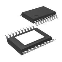
PIN CONFIGURATIONS
TSSOP-20
PWP
(TOP VIEW)
GND/HEATSINK
1
20
GND/HEATSINK
NC
2
19
NC
IN
3
18
NC
IN
4
17
GND
EN
5
16
NC
PG or RESET
6
15
NC
FB/SENSE
7
14
NC
OUTPUT
8
13
NC
OUTPUT
9
12
NC
10
11
GND/HEATSINK
GND/HEATSINK
Table 1. PIN DESCRIPTIONS
TPS751xxQ, TPS753xxQ
6
NAME
TSSOP-20 (PWP)
PIN NO.
I/O
EN
5
I
Negative polarity enable (EN) input
FB/SENSE
7
I
Adjustable voltage version only; feedback voltage for setting output voltage of
the device. Not internally connected on adjustable versions. Sense input for
fixed options.
GND
17
GND/HEATSINK
1, 10, 11, 20
Ground
Ground/heatsink
IN
3, 4
NC
2, 12, 13, 14,
15, 16, 18, 19
OUTPUT
8, 9
O
PG/RESET
6
O
Submit Documentation Feedback
DESCRIPTION
I
Input voltage
Not connected
Regulated output voltage
TPS751xxQ devices only; open-drain power-good (PG) output.
TPS753xxQ devices only; open-drain RESET output.
Copyright © 2000–2007, Texas Instruments Incorporated
�TPS751xxQ
TPS753xxQ
www.ti.com
SLVS241C – MARCH 2000 – REVISED OCTOBER 2007
TPS753xxQ RESET Timing Diagram
VIN
Vres
(1)
Vres
t
VOUT
VIT+
(2)
(2)
VIT+
Threshold
Voltage
(2)
VIT-
Less than 5% of the
Output Voltage
(2)
VIT-
t
RESET
Output
100 ms
Delay
100 ms
Delay
Output
Undefined
Output
Undefined
t
(1)
Vres is the minimum input voltage for a valid RESET. The symbol Vres is not currently listed within EIA or JEDEC
standards for semiconductor symbology.
(2)
VIT: Trip voltage is typically 5% lower than the output voltage (95% VOUT). VIT– to VIT+ is the hysteresis voltage.
TPS751xxQ Power Good Timing Diagram
VIN
(1)
VPG
VPG
t
VOUT
VIT+
(2)
(2)
VIT+
Threshold
Voltage
(2)
VIT-
(2)
VIT-
t
PG
Output
Output
Undefined
Output
Undefined
t
(1)
VPG is the minimum input voltage for a valid Power Good. The symbol VPG is not currently listed within EIA or JEDEC
standards for semiconductor symbology.
(2)
VIT: Trip voltage is typically 17% lower than the output voltage (83% VOUT). VIT– to VIT+ is the hysteresis voltage.
Copyright © 2000–2007, Texas Instruments Incorporated
Submit Documentation Feedback
7
�TPS751xxQ
TPS753xxQ
www.ti.com
SLVS241C – MARCH 2000 – REVISED OCTOBER 2007
TYPICAL CHARACTERISTICS
Table of Graphs
FIGURE NO.
8
vs Output Current
Figure 3, Figure 4
VOUT
Output Voltage
vs Junction Temperature
Figure 5, Figure 6
vs Time
Figure 18
IGND
Ground Current
vs Junction Temperature
Figure 7
PSRR
Power-Supply Ripple Rejection
vs Frequency
Figure 8
Output Spectral Noise Density
vs Frequency
Figure 9
ZOUT
Output Impedance
vs Frequency
Figure 10
VDO
Dropout Voltage
vs Input Voltage
Figure 11
vs Junction Temperature
Figure 12
VIN
Input Voltage (Min)
LINE
Line Transient Response
Figure 14, Figure 16
LOAD
Load Transient Response
Figure 15, Figure 17
ESR
Equivalent Series Resistance
Submit Documentation Feedback
vs Output Voltage
vs Output Current
Figure 13
Figure 20, Figure 21
Copyright © 2000–2007, Texas Instruments Incorporated
�TPS751xxQ
TPS753xxQ
www.ti.com
SLVS241C – MARCH 2000 – REVISED OCTOBER 2007
TYPICAL CHARACTERISTICS
Over operating temperature range (TJ= –40°C to +125°C) unless otherwise noted. Typical values are at TJ = +25°C.
TPS75x33Q
OUTPUT VOLTAGE
vs OUTPUT CURRENT
TPS75x15Q
OUTPUT VOLTAGE
vs OUTPUT CURRENT
3.305
1.503
VIN = 2.7 V
TJ = +25°C
VIN = 4.3 V
TJ = +25°C
1.502
VOUT
VOUT - Output Voltage - V
VOUT - Output Voltage - V
3.303
VOUT
3.301
3.299
1.501
1.5
1.499
3.297
1.498
3.295
0
1000
500
1.497
1500
0
500
IOUT - Output Current - mA
1000
1500
IOUT - Output Current - mA
Figure 3.
Figure 4.
TPS75x33Q
OUTPUT VOLTAGE
vs JUNCTION TEMPERATURE
TPS75x15Q
OUTPUT VOLTAGE
vs JUNCTION TEMPERATURE
3.37
1.53
VIN = 4.3 V
VIN = 2.7 V
3.35
1.52
VOUT - Output Voltage - V
VOUT - Output Voltage - V
1 mA
3.33
1 mA
3.31
3.29
1.5 A
3.27
1.50
1.5 A
1.49
1.48
3.25
3.23
-40
1.51
10
60
110
TJ - Junction Temperature - °C
Figure 5.
Copyright © 2000–2007, Texas Instruments Incorporated
160
1.47
-40
10
60
110
160
TJ - Junction Temperature - °C
Figure 6.
Submit Documentation Feedback
9
�TPS751xxQ
TPS753xxQ
www.ti.com
SLVS241C – MARCH 2000 – REVISED OCTOBER 2007
TYPICAL CHARACTERISTICS (continued)
Over operating temperature range (TJ= –40°C to +125°C) unless otherwise noted. Typical values are at TJ = +25°C.
TPS75xxxQ
GROUND CURRENT
vs JUNCTION TEMPERATURE
85
100
VIN = 5 V
IOUT = 1.5 A
PSRR - Power-Supply Rejection Ratio - dB
90
TPS75x33Q
POWER-SUPPLY RIPPLE REJECTION
vs FREQUENCY
Ground Current - mA
80
75
70
65
60
55
50
-40
90
VIN = 4.3 V
COUT = 100 mF
IOUT = 1 mA
TJ = +25°C
80
70
60
50
40
30
20
VIN = 4.3 V
COUT = 100 mF
IOUT = 1.5 A
TJ = +25°C
10
10
60
110
0
10
160
100
100k
Figure 8.
TPS75x33Q
OUTPUT SPECTRAL NOISE DENSITY
vs FREQUENCY
TPS75x33Q
OUTPUT IMPEDANCE
vs FREQUENCY
10
VIN = 4.3 V
VOUT = 3.3 V
COUT = 100 mF
TJ = +25°C
1M
10M
1M
10M
1
COUT = 100 mF
IOUT = 1 mA
ZOUT - Output Impedance - W
Vn - Voltage Noise - nV/ÖHz
1.6
10k
Figure 7.
2.0
1.8
1k
f - Frequency - Hz
TJ - Junction Temperature - °C
1.4
IOUT = 1.5 A
1.2
1.0
0.8
0.6
1
10
-1
COUT = 100 mF
IOUT = 1.5 A
0.4
0.2
0
10
10
IOUT = 1 mA
100
1k
10k
50k
10
-2
10
100
1k
10k
100k
f - Frequency - Hz
f - Frequency - Hz
Figure 9.
Figure 10.
Submit Documentation Feedback
Copyright © 2000–2007, Texas Instruments Incorporated
�TPS751xxQ
TPS753xxQ
www.ti.com
SLVS241C – MARCH 2000 – REVISED OCTOBER 2007
TYPICAL CHARACTERISTICS (continued)
Over operating temperature range (TJ= –40°C to +125°C) unless otherwise noted. Typical values are at TJ = +25°C.
TPS75x01Q
DROPOUT VOLTAGE
vs INPUT VOLTAGE
TPS75x33Q
DROPOUT VOLTAGE
vs JUNCTION TEMPERATURE
300
300
IOUT = 1.5 A
250
VDO - Dropout Voltage - mV
VDO - Dropout Voltage - mV
250
TJ = +125°C
200
150
TJ = +25°C
TJ = -40°C
100
200
IOUT = 1.5 A
150
100
IOUT = 0.5 A
50
50
0
0
2.5
3.5
3
4.5
4
5
10
-40
VIN - Input Voltage - V
60
110
160
TJ - Junction Temperature - °C
Figure 11.
Figure 12.
INPUT VOLTAGE (MIN)
vs OUTPUT VOLTAGE
TPS75x15Q
LINE TRANSIENT RESPONSE
4.0
DVOUT - Change in
Output Voltage - mV
TA = +25°C
TA = +125°C
TA = -40°C
2.7
2.0
1.5
IOUT = 1.5 A
COUT = 100 mF
VOUT = 1.5 V
dV = 1 V
ms
dT
100
0
-100
3.0
VIN - Input Voltage - V
VIN - Input Voltage (Min) - V
IOUT = 1.5 A
1.75
2
2.25
2.5
2.75
VOUT - Output Voltage - V
Figure 13.
Copyright © 2000–2007, Texas Instruments Incorporated
3
3.25
3.5
4
3
0
0.1
0.2
0.3
0.4
0.5
0.6
0.7
0.8
0.9
1.0
t - Time - ms
Figure 14.
Submit Documentation Feedback
11
�TPS751xxQ
TPS753xxQ
www.ti.com
SLVS241C – MARCH 2000 – REVISED OCTOBER 2007
TYPICAL CHARACTERISTICS (continued)
Over operating temperature range (TJ= –40°C to +125°C) unless otherwise noted. Typical values are at TJ = +25°C.
TPS75x33Q
LINE TRANSIENT RESPONSE
ILOAD = 1.5 A
CLOAD = 100 mF (Tantalum)
VOUT = 1.5 V
50
DVOUT - Change in
Output Voltage - mV
DVOUT - Change in
Output Voltage - mV
TPS75x15Q
LOAD TRANSIENT RESPONSE
0
-50
dV = 1 V
ms
dT
100
0
-100
VIN - Input Voltage - V
-100
IOUT - Output Current - A
IOUT = 1.5 A
COUT = 100 mF (Tantalum)
VOUT = 3.3 V
-150
1.5
5.3
4.3
0
1
2
3
4
5
6
7
8
9
0.3
0.4
0.5
0.6
0.7
0.8
t - Time - ms
Figure 16.
TPS75x33Q
LOAD TRANSIENT RESPONSE
TPS75x33QOUTPUT VOLTAGE
vs TIME (AT STARTUP)
0
-50
0.9
1.0
VIN = 4.3 V
TJ = +25°C
3.3
0
Enable Voltage - V
IOUT - Output Current - A
0.2
Figure 15.
-100
-150
1.5
0
0
1
2
3
4
5
6
t - Time - ms
Figure 17.
12
0.1
t - Time - ms
ILOAD = 1.5 A
CLOAD = 100 mF (Tantalum)
VOUT = 3.3 V
50
0
10
VOUT - Output Voltage - V
DVOUT - Change in
Output Voltage - mV
0
Submit Documentation Feedback
7
8
9
10
4.3
0
0
0.2
0.4
0.6
0.8
1.0
t - Time - ms
Figure 18.
Copyright © 2000–2007, Texas Instruments Incorporated
�TPS751xxQ
TPS753xxQ
www.ti.com
SLVS241C – MARCH 2000 – REVISED OCTOBER 2007
TYPICAL CHARACTERISTICS (continued)
Over operating temperature range (TJ= –40°C to +125°C) unless otherwise noted. Typical values are at TJ = +25°C.
Test Circuit for Typical Regions of Stability (Figure 20 and Figure 21) (Fixed Output Options)
VIN
To Load
IN
OUT
+
COUT
EN
RL
GND
ESR
Figure 19.
TYPICAL REGION OF STABILITY
EQUIVALENT SERIES RESISTANCE(1)
vs OUTPUT CURRENT
TYPICAL REGION OF STABILITY
EQUIVALENT SERIES RESISTANCE(1)
vs OUTPUT CURRENT
10
VOUT = 3.3 V
COUT = 100 mF
VIN = 4.3 V
TJ = +25°C
ESR -Equivalent Series Resistance- W
ESR -Equivalent Series Resistance- W
10
1
Region of Stability
0.1
0.05
VOUT = 3.3 V
COUT = 47 mF
VIN = 4.3 V
TJ = +25°C
1
Region of Stability
0.1
Region of Instability
Region of Instability
0.01
0.01
0
0.5
1.0
1.5
0
0.5
1.0
IOUT - Output Current - A
IOUT - Output Current - A
Figure 20.
Figure 21.
1.5
(1). Equivalent series resistance (ESR) refers to the total series resistance, including the ESR of the capacitor,
any series resistance added externally, and PWB trace resistance to COUT.
Copyright © 2000–2007, Texas Instruments Incorporated
Submit Documentation Feedback
13
�TPS751xxQ
TPS753xxQ
www.ti.com
SLVS241C – MARCH 2000 – REVISED OCTOBER 2007
APPLICATION INFORMATION
The TPS751xxQ and TPS753xxQ devices include four fixed-output voltage regulators (1.5 V, 1.8 V, 2.5 V and
3.3 V), and an adjustable regulator, the TPS75x01Q (adjustable from 1.5 V to 5 V).
Minimum Load Requirements
The TPS751xxQ and TPS753xxQ families are stable even at zero load; no minimum load is required for
operation.
Pin Functions
Enable (EN)
The EN terminal is an input that enables or shuts down the device. If EN is a logic high, the device is in
shutdown mode. When EN goes to logic low, then the device is enabled.
Power-Good (PG)—TPS751xxQ
The PG terminal is an open drain, active high output that indicates the status of VOUT (output of the LDO). When
VOUT reaches 83% of the regulated voltage, PG goes to a high impedance state. It goes to a low-impedance
state when VOUT falls below 83% (that is, an overload condition) of the regulated voltage. The open drain output
of the PG terminal requires a pullup resistor.
Sense (SENSE)
The SENSE terminal of the fixed output options must be connected to the regulator output, and the connection
should be as short as possible. Internally, SENSE connects to a high-impedance wide-bandwidth amplifier
through a resistor-divider network, and noise pickup feeds through to the regulator output. It is essential to route
the SENSE connection in such a way to minimize/avoid noise pickup. Adding RC networks between the SENSE
terminal and VOUT to filter noise is not recommended because these types of networks may cause the regulator
to oscillate.
Reset (RESET)—TPS753xxQ
The RESET terminal is an open drain, active low output that indicates the status of VOUT. When VOUT reaches
95% of the regulated voltage, RESET goes to a high-impedance state after a 100-ms delay. RESET goes to a
low-impedance state when VOUT is below 95% of the regulated voltage. The open-drain output of the RESET
terminal requires a pullup resistor.
GND/HEATSINK
All GND/HEATSINK terminals are connected directly to the mount pad for thermal-enhanced operation. These
terminals could be connected to GND or left floating.
Input Capacitor
For a typical application, an input bypass capacitor (0.22 μF to 1 μF) is recommended for device stability. This
capacitor should be as close to the input pins as possible. For fast transient conditions where droop at the input
of the LDO may occur because of high inrush current, it is recommended to place a larger capacitor at the input
as well. The size of this capacitor depends on the output current and response time of the main power supply, as
well as the distance to the load (LDO).
Output Capacitor
As with most LDO regulators, the TPS751xxQ and TPS753xxQ require an output capacitor connected between
OUT and GND to stabilize the internal control loop. The minimum recommended capacitance value is 47 μF and
the ESR (equivalent series resistance) must be between 100 mΩ and 10 Ω. Solid tantalum electrolytic, aluminum
electrolytic, and multilayer ceramic capacitors are all suitable, provided they meet the requirements described in
this section. Larger capacitors provide a wider range of stability and better load transient response.
14
Submit Documentation Feedback
Copyright © 2000–2007, Texas Instruments Incorporated
�TPS751xxQ
TPS753xxQ
www.ti.com
SLVS241C – MARCH 2000 – REVISED OCTOBER 2007
This information, along with the ESR graphs (see Figure 20 and Figure 21), is included to assist in selection of
suitable capacitance for the user’s application. When necessary to achieve low height requirements along with
high output current and/or high load capacitance, several higher ESR capacitors can be used in parallel to meet
these guidelines.
ESR and Transient Response
LDOs typically require an external output capacitor for stability. In fast transient response applications, capacitors
are used to support the load current while the LDO amplifier is responding. In most applications, one capacitor is
used to support both functions.
Besides its capacitance, every capacitor also contains parasitic impedances. These parasitic impedances are
resistive as well as inductive. The resistive impedance is called equivalent series resistance (ESR), and the
inductive impedance is called equivalent series inductance (ESL). The equivalent schematic diagram of any
capacitor can therefore be drawn as shown in Figure 22.
RESR
LESL
C
Figure 22. ESR and ESL
In most cases one can neglect the effect of inductive impedance ESL. Therefore, the following application
focuses mainly on the parasitic resistance ESR..
Figure 23 shows the output capacitor and its parasitic impedances in a typical LDO output stage.
IOUT
LDO
+
VESR
RESR
–
VIN
RLOAD
VOUT
COUT
Figure 23. LDO Output Stage With Parasitic Resistances ESR and ESL
Copyright © 2000–2007, Texas Instruments Incorporated
Submit Documentation Feedback
15
�TPS751xxQ
TPS753xxQ
www.ti.com
SLVS241C – MARCH 2000 – REVISED OCTOBER 2007
In steady state operation (dc state condition), the load current is supplied by the LDO (solid arrow) and the
voltage across the capacitor is the same as the output voltage (V(COUT) = VOUT). This condition means that no
current is flowing into the COUT branch. If IOUT suddenly increases (that is, a transient condition), the following
events occur:
• The LDO is not able to supply the sudden current need because of its response time (t1 in Figure 24).
Therefore, capacitor COUT provides the current for the new load condition (the dashed arrow). COUT now acts
like a battery with an internal resistance, ESR. Depending on the current demand at the output, a voltage
drop occurs at RESR. This voltage is shown as VESR in Figure 23.
• When COUT is conducting current to the load, initial voltage at the load is VOUT = V(COUT) – VESR. As a result
of the discharge of COUT, the output voltage VOUT drops continuously until the response time t1 of the LDO is
reached and the LDO resumes supplying the load. From this point, the output voltage starts rising again until
it reaches the regulated voltage. This period is shown as t2 in Figure 24.
Figure 24 also shows the impact of different ESRs on the output voltage. The left brackets show different levels
of ESRs where number 1 displays the lowest and number 3 displays the highest ESR.
From the above discussion, the following conclusions can be drawn:
• The higher the ESR, the larger the droop at the beginning of load transient.
• The smaller the output capacitor, the faster the discharge time and the bigger the voltage droop during the
LDO response period.
Conclusion
To minimize the transient output droop, capacitors must have a low ESR and be large enough to support the
minimum output voltage requirement.
IOUT
VOUT
1
2
ESR 1
3
ESR 2
ESR 3
t1
t2
Figure 24. Correlation of Different ESRs and Their Influence to the Regulation of VOUT at a Load Step
From Low-to-High Output Current
16
Submit Documentation Feedback
Copyright © 2000–2007, Texas Instruments Incorporated
�TPS751xxQ
TPS753xxQ
www.ti.com
SLVS241C – MARCH 2000 – REVISED OCTOBER 2007
Programming the TPS75x01Q Adjustable LDO Regulator
The output voltage of the TPS77x01Q adjustable regulator is programmed using an external resistor divider as
shown in Figure 25. The output voltage is calculated using Equation 1:
R
VOUT = Vref ´ (1 + 1 )
R2
(1)
Where:
•
Vref = 1.1834 V typ (the internal reference voltage)
Resistors R1 and R2 should be chosen for approximately 40μA divider current. Lower value resistors can be
used, but offer no inherent advantage and waste more power. Higher values should be avoided as leakage
currents at FB increase the output voltage error. The recommended design procedure is to choose R2 = 30.1 kΩ
to set the divider current at approximately 40μA and then calculate R1 using Equation 2:
V
R1 = ( OUT - 1) ´ R2
Vref
(2)
OUTPUT VOLTAGE
PROGRAMMING GUIDE
TPS75x01Q
VIN
IN
0.22 mF
PG/
RESET
PG or RESET Output
250 kW
VOUT
OUT
> 2.0 V
R1
EN
< 0.7 V
FB/SENSE
GND
COUT
R2
OUTPUT
VOLTAGE
R1
R2
UNIT
2.5 V
33.2
30.1
kW
3.3 V
53.6
30.1
kW
3.6 V
61.9
30.1
kW
NOTE: To reduce noise and prevent oscillation,
R1 and R2 must be as close as possible to the
FB/SENSE terminal.
Figure 25. TPS75x01Q Adjustable LDO Regulator Programming
Regulator Protection
The TPS751xxQ and TPS753xxQ PMOS-pass transistors have a built-in back diode that conducts reverse
currents when the input voltage drops below the output voltage (for example, during power down). Current is
conducted from the output to the input and is not internally limited. When extended reverse voltage is anticipated,
external limiting may be appropriate.
The TPS751xxQ and TPS753xxQ also feature internal current limiting and thermal protection. During normal
operation, the TPS751xxQ and TPS753xxQ limit output current to approximately 3.3 A. When current limiting
engages, the output voltage scales back linearly until the overcurrent condition ends. While current limiting is
designed to prevent gross device failure, care should be taken not to exceed the power dissipation ratings of the
package. If the temperature of the device exceeds +150°C (typ), thermal-protection circuitry shuts it down. Once
the device has cooled below +130°C (typ), regulator operation resumes.
Copyright © 2000–2007, Texas Instruments Incorporated
Submit Documentation Feedback
17
�TPS751xxQ
TPS753xxQ
www.ti.com
SLVS241C – MARCH 2000 – REVISED OCTOBER 2007
Power Dissipation and Junction Temperature
Specified regulator operation is assured to a junction temperature of +125°C; the maximum junction temperature
should be restricted to +125°C under normal operating conditions. This restriction limits the power dissipation the
regulator can handle in any given application. To ensure the junction temperature is within acceptable limits,
calculate the maximum allowable dissipation, PD(max), and the actual dissipation, PD, which must be less than or
equal to PD(max).
The maximum-power-dissipation limit is determined using Equation 3:
TJ(Max) - TA
PD(Max) =
RqJA
(3)
where:
•
•
•
TJ(max) is the maximum allowable junction temperature
RθJA is the thermal resistance junction-to-ambient for the package; that is, 34.6°C/W for the 20-terminal PWP
with no airflow (see Dissipation Ratings Table).
TA is the ambient temperature
The regulator dissipation is calculated using Equation 4:
PD = (VIN - VOUT) ´ IOUT
(4)
Power dissipation resulting from quiescent current is negligible. Excessive power dissipation triggers the thermal
protection circuit.
THERMAL INFORMATION
Thermally-Enhanced TSSOP-20 (PWP–PowerPAD)
The thermally-enhanced PWP package is based on the 20-pin TSSOP, but includes a thermal pad [see
Figure 26(c)] to provide an effective thermal contact between the IC and the printed wiring board (PWB).
DIE
(a) Side View
Thermal
Pad
DIE
(b) End View
(c) Bottom View
Figure 26. Views of Thermally-Enhanced PWP Package
Traditionally, surface mount and power have been mutually exclusive terms. A variety of scaled-down
TO220-type packages have leads formed as gull wings to make them applicable for surface-mount applications.
These packages, however, suffer from several shortcomings: they do not address the very low profile
requirements (less than 2 mm) of many of today’s advanced systems, and they do not offer a pin-count high
enough to accommodate increasing integration. On the other hand, traditional low-power surface-mount
packages require power dissipation derating that severely limits the usable range of many high-performance
analog circuits.
The PWP package (a thermally-enhanced TSSOP) combines fine-pitch surface-mount technology with thermal
performance comparable to much larger power packages.
18
Submit Documentation Feedback
Copyright © 2000–2007, Texas Instruments Incorporated
�TPS751xxQ
TPS753xxQ
www.ti.com
SLVS241C – MARCH 2000 – REVISED OCTOBER 2007
The PWP package is designed to optimize the heat transfer to the PWB. Because of the very small size and
limited mass of a TSSOP package, thermal enhancement is achieved by improving the thermal conduction paths
that remove heat from the component. The thermal pad is formed using a lead-frame design (patent pending)
and manufacturing technique to provide the user with direct connection to the heat-generating IC. When this pad
is soldered or otherwise coupled to an external heat dissipator, high power dissipation in the ultra-thin, fine-pitch,
surface-mount package can be reliably achieved.
Because the conduction path has been enhanced, power-dissipation capability is determined by the thermal
considerations in the PWB design. For example, simply adding a localized copper plane (heatsink surface) that is
coupled to the thermal pad enables the PWP package to dissipate 2.5 W in free air (see Figure 28(a), 8 cm2 of
copper heatsink and natural convection). Increasing the heatsink size increases the power dissipation range for
the component. The power dissipation limit can be further improved by adding airflow to a PWB/IC assembly
(see Figure 27 and Figure 28). The line drawn at 0.3 cm2 in Figure 27 and Figure 28 indicates performance at
the minimum recommended heatsink size, illustrated in Figure 30.
The thermal pad is directly connected to the substrate of the IC, which for the TPS751xxQPWP and
TPS753xxQPWP series is a secondary electrical connection to device ground. The heat-sink surface that is
added to the PWP can be a ground plane or left electrically isolated. In TO220-type surface-mount packages, the
thermal connection is also the primary electrical connection for a given terminal which is not always ground. The
PWP package provides up to 16 independent leads that can be used as inputs and outputs. (Note: leads 1, 10,
11, and 20 are internally connected to the thermal pad and the IC substrate.)
150
RqJA - Thermal Resistance - °C/W
Natural Convection
50 ft/min
100 ft/min
100
150 ft/min
200 ft/min
75
50
250 ft/min
300 ft/min
25
0 0.3
1
2
3
4
6
5
Copper Heatsink Area - cm
7
8
2
Figure 27. Thermal Resistance vs Copper Heatsink Area
Copyright © 2000–2007, Texas Instruments Incorporated
Submit Documentation Feedback
19
�TPS751xxQ
TPS753xxQ
www.ti.com
SLVS241C – MARCH 2000 – REVISED OCTOBER 2007
3.5
3.5
TA = +25°C
TA = +55°C
300 ft/min
3.0
PD - Power Dissipation Limit - W
PD - Power Dissipation Limit - W
3.0
150 ft/min
2.5
2.0
Natural Convection
1.5
1.0
0.5
300 ft/min
2.5
2.0
150 ft/min
1.5
Natural Convection
1.0
0.5
0
0 0.3
2
6
4
Copper Heatsink Area - cm
0
8
0 0.3
2
2
4
Copper Heatsink Area - cm
(a)
6
8
2
(b)
3.5
TA = +105°C
PD - Power Dissipation Limit - W
3.0
2.5
2.0
1.5
150 ft/min
300 ft/min
1.0
Natural Convection
0.5
0
0 0.3
2
4
Copper Heatsink Area - cm
6
8
2
(c)
Figure 28. Power Ratings of the PWP Package at Ambient Temperatures of +25°C, +55°C, and +105°C
20
Submit Documentation Feedback
Copyright © 2000–2007, Texas Instruments Incorporated
�TPS751xxQ
TPS753xxQ
www.ti.com
SLVS241C – MARCH 2000 – REVISED OCTOBER 2007
Figure 29 is an example of a thermally-enhanced PWB layout for use with the new PWP package. This board
configuration was used in the thermal experiments that generated the power ratings shown in Figure 27 and
Figure 28. As discussed earlier, copper has been added on the PWB to conduct heat away from the device. RθJA
for this assembly is illustrated in Figure 27 as a function of heatsink area. A family of curves is included to
illustrate the effect of airflow introduced into the system.
Heatsink Area
1 oz Copper
Board thickness
62 mils (0.15748 cm)
Board size
3.2 in. x 3.2 in.
Board material
FR4
Copper trace/heatsink
1 oz
Exposed pad mounting
63/67 tin/lead (Sn/Pb) solder
Figure 29. PWB Layout (Including Copper Heatsink Area) for Thermally-Enhanced PWP Package
From Figure 27, RθJA for a PWB assembly can be determined and used to calculate the maximum
power-dissipation limit for the component/PWB assembly, with the equation:
TJ(Max) - TA
PD(Max) =
RqJA (System)
(5)
Where TJmax is the maximum specified junction temperature (+150°C absolute maximum limit, +125°C
recommended operating limit) and TA is the ambient temperature.
PD(max) should then be applied to the internal power dissipated by the TPS75133QPWP regulator. The equation
for calculating total internal power dissipation of the TPS75133QPWP is:
PD(total) = (VIN - VOUT) ´ IOUT + VIN ´ IQ
(6)
Because the quiescent current of the TPS75133QPWP is very low, the second term is negligible, further
simplifying the equation to:
PD(total) = (VIN - VOUT) ´ IOUT
(7)
For the case where TA = +55°C, airflow = 200 ft/min, copper heat-sink area = 4 cm2, the maximum
power-dissipation limit can be calculated. First, from Figure 27, we find the system RθJA is 50°C/W; therefore, the
maximum power-dissipation limit is:
TJ(Max) - TA 125°C - 55°C
=
= 1.4 W
PD(Max) =
RqJA (System)
50°C/W
(8)
If the system implements a TPS75133QPWP regulator, where VIN = 5 V and IOUT = 800 mA, the internal power
dissipation is:
PD(total) = (VIN - VOUT) ´ IOUT = (5 - 3.3) ´ 0.8 = 1.36 W
(9)
Comparing PD(total) with PD(max) reveals that the power dissipation in this example does not exceed the calculated
limit. When it does, one of two corrective actions should be made: either raise the power-dissipation limit by
increasing the airflow or the heat-sink area, or loweri the internal power dissipation of the regulator by reducing
the input voltage or the load current. In either case, the above calculations should be repeated with the new
system parameters.
Copyright © 2000–2007, Texas Instruments Incorporated
Submit Documentation Feedback
21
�TPS751xxQ
TPS753xxQ
www.ti.com
SLVS241C – MARCH 2000 – REVISED OCTOBER 2007
Mounting Information
The primary requirement is to complete the thermal contact between the thermal pad and the PWB metal. The
thermal pad is a solderable surface and is fully intended to be soldered at the time the component is mounted.
Although voiding in the thermal-pad solder-connection is not desirable, up to 50% voiding is acceptable. The data
included in Figure 27 and Figure 28 are for soldered connections with voiding between 20% and 50%. The
thermal analysis shows no significant difference resulting from the variation in voiding percentage.
Figure 30 shows the solder-mask land pattern for the PWP package. The minimum recommended heat-sink area
is also illustrated. This is simply a copper plane under the body extent of the package, including metal routed
under terminals 1, 10, 11, and 20.
Minimum Recommended
Heatsink Area
Location of Exposed
Thermal Pad on
PWP Package
Figure 30. PWP Package Land Pattern
22
Submit Documentation Feedback
Copyright © 2000–2007, Texas Instruments Incorporated
�PACKAGE OPTION ADDENDUM
www.ti.com
14-Oct-2022
PACKAGING INFORMATION
Orderable Device
Status
(1)
Package Type Package Pins Package
Drawing
Qty
Eco Plan
(2)
Lead finish/
Ball material
MSL Peak Temp
Op Temp (°C)
Device Marking
(3)
Samples
(4/5)
(6)
TPS75101QPWP
ACTIVE
HTSSOP
PWP
20
70
RoHS & Green
NIPDAU
Level-2-260C-1 YEAR
-40 to 125
PT75101
Samples
TPS75101QPWPR
ACTIVE
HTSSOP
PWP
20
2000
RoHS & Green
NIPDAU
Level-2-260C-1 YEAR
-40 to 125
PT75101
Samples
TPS75115QPWP
ACTIVE
HTSSOP
PWP
20
70
RoHS & Green
NIPDAU
Level-2-260C-1 YEAR
-40 to 125
PT75115
Samples
TPS75115QPWPR
ACTIVE
HTSSOP
PWP
20
2000
RoHS & Green
NIPDAU
Level-2-260C-1 YEAR
-40 to 125
PT75115
Samples
TPS75118QPWP
ACTIVE
HTSSOP
PWP
20
70
RoHS & Green
NIPDAU
Level-2-260C-1 YEAR
-40 to 125
PT75118
Samples
TPS75118QPWPR
ACTIVE
HTSSOP
PWP
20
2000
RoHS & Green
NIPDAU
Level-2-260C-1 YEAR
-40 to 125
PT75118
Samples
TPS75125QPWP
ACTIVE
HTSSOP
PWP
20
70
RoHS & Green
NIPDAU
Level-2-260C-1 YEAR
-40 to 125
PT75125
Samples
TPS75125QPWPG4
ACTIVE
HTSSOP
PWP
20
70
RoHS & Green
NIPDAU
Level-2-260C-1 YEAR
-40 to 125
PT75125
Samples
TPS75125QPWPR
ACTIVE
HTSSOP
PWP
20
2000
RoHS & Green
NIPDAU
Level-2-260C-1 YEAR
-40 to 125
PT75125
Samples
TPS75133QPWP
ACTIVE
HTSSOP
PWP
20
70
RoHS & Green
NIPDAU
Level-2-260C-1 YEAR
-40 to 125
PT75133
Samples
TPS75133QPWPR
ACTIVE
HTSSOP
PWP
20
2000
RoHS & Green
NIPDAU
Level-2-260C-1 YEAR
-40 to 125
PT75133
Samples
TPS75301QPWP
ACTIVE
HTSSOP
PWP
20
70
RoHS & Green
NIPDAU
Level-2-260C-1 YEAR
-40 to 125
PT75301
Samples
TPS75301QPWPR
ACTIVE
HTSSOP
PWP
20
2000
RoHS & Green
NIPDAU
Level-2-260C-1 YEAR
-40 to 125
PT75301
Samples
TPS75315QPWP
ACTIVE
HTSSOP
PWP
20
70
RoHS & Green
NIPDAU
Level-2-260C-1 YEAR
-40 to 125
PT75315
Samples
TPS75318QPWP
ACTIVE
HTSSOP
PWP
20
70
RoHS & Green
NIPDAU
Level-2-260C-1 YEAR
-40 to 125
PT75318
Samples
TPS75318QPWPR
ACTIVE
HTSSOP
PWP
20
2000
RoHS & Green
NIPDAU
Level-2-260C-1 YEAR
-40 to 125
PT75318
Samples
TPS75325QPWP
ACTIVE
HTSSOP
PWP
20
70
RoHS & Green
NIPDAU
Level-2-260C-1 YEAR
-40 to 125
PT75325
Samples
TPS75325QPWPR
ACTIVE
HTSSOP
PWP
20
2000
RoHS & Green
NIPDAU
Level-2-260C-1 YEAR
-40 to 125
PT75325
Samples
TPS75333QPWP
ACTIVE
HTSSOP
PWP
20
70
RoHS & Green
NIPDAU
Level-2-260C-1 YEAR
-40 to 125
PT75333
Samples
TPS75333QPWPR
ACTIVE
HTSSOP
PWP
20
2000
RoHS & Green
NIPDAU
Level-2-260C-1 YEAR
-40 to 125
PT75333
Samples
Addendum-Page 1
�PACKAGE OPTION ADDENDUM
www.ti.com
14-Oct-2022
(1)
The marketing status values are defined as follows:
ACTIVE: Product device recommended for new designs.
LIFEBUY: TI has announced that the device will be discontinued, and a lifetime-buy period is in effect.
NRND: Not recommended for new designs. Device is in production to support existing customers, but TI does not recommend using this part in a new design.
PREVIEW: Device has been announced but is not in production. Samples may or may not be available.
OBSOLETE: TI has discontinued the production of the device.
(2)
RoHS: TI defines "RoHS" to mean semiconductor products that are compliant with the current EU RoHS requirements for all 10 RoHS substances, including the requirement that RoHS substance
do not exceed 0.1% by weight in homogeneous materials. Where designed to be soldered at high temperatures, "RoHS" products are suitable for use in specified lead-free processes. TI may
reference these types of products as "Pb-Free".
RoHS Exempt: TI defines "RoHS Exempt" to mean products that contain lead but are compliant with EU RoHS pursuant to a specific EU RoHS exemption.
Green: TI defines "Green" to mean the content of Chlorine (Cl) and Bromine (Br) based flame retardants meet JS709B low halogen requirements of


 工商网监
湘ICP备2023018690号
工商网监
湘ICP备2023018690号
