TPS75801,, TPS758A01
TPS75815, TPS75818
TPS75825, TPS75833
www.ti.com
SLVS330F – JUNE 2001 – REVISED APRIL 2007
FAST-TRANSIENT RESPONSE, 3A, LOW-DROPOUT VOLTAGE REGULATORS
•
•
•
•
•
•
•
3A Low-Dropout Voltage Regulator
Available in 1.5V, 1.8V, 2.5V, and 3.3V
Fixed-Output and Adjustable Versions
Dropout Voltage Typically 150mV at 3A
(TPS75833)
VREF and Pinout Compatible with MIC29302
(TPS758A01)
Low 125µA Typical Quiescent Current
Fast Transient Response
3% Tolerance Over Specified Conditions for
Fixed-Output Versions
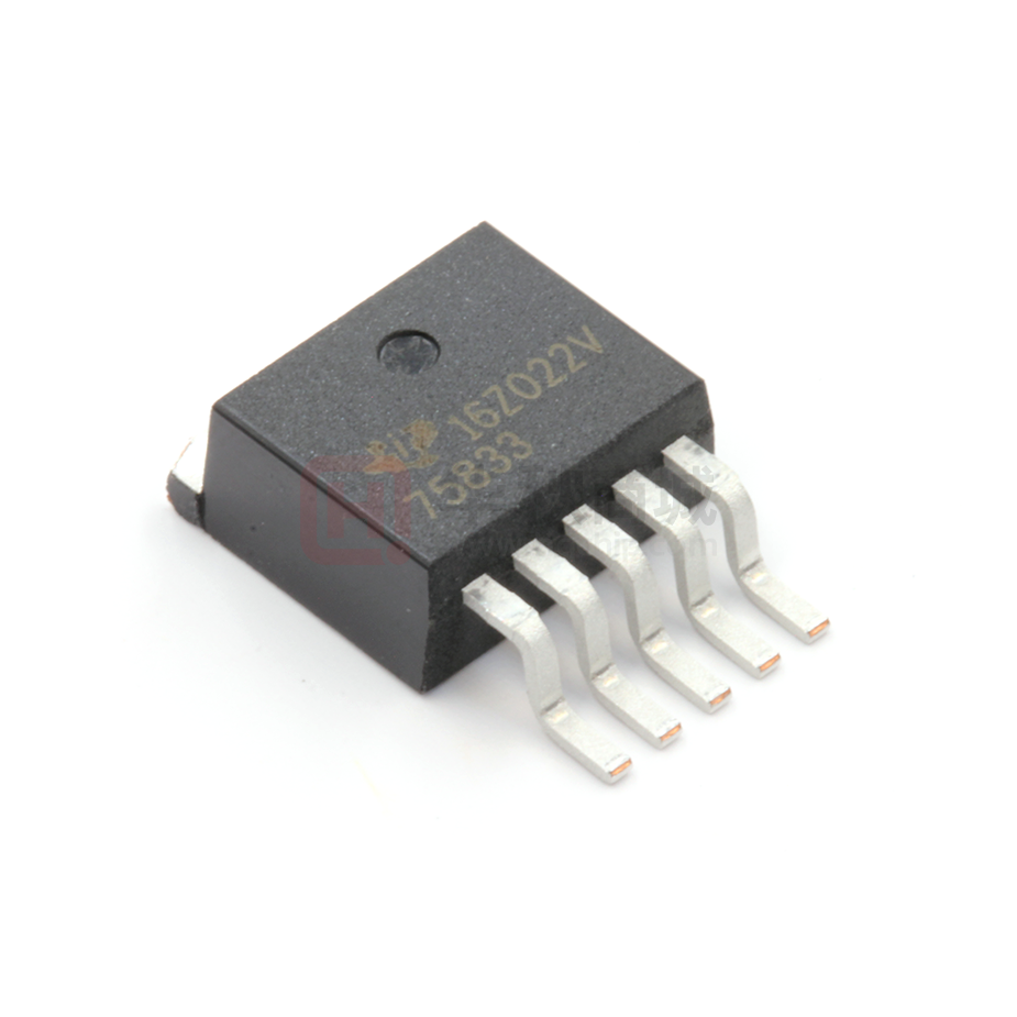
Available in 5-Pin TO-220 and TO-263
Surface-Mount Packages
Thermal Shutdown Protection
DESCRIPTION
The TPS758xx family of 3A low dropout (LDO)
regulators contains four fixed voltage option
regulators and an adjustable voltage option
regulator. These devices are capable of supplying 3A
of output current with a dropout of 150mV
(TPS75833). Therefore, the device is capable of
performing a 3.3V to 2.5V conversion.
TO−220 (KC) PACKAGE
(TOP VIEW)
1
2
3
4
5
TO−263 (KTT) PACKAGE
(TOP VIEW)
EN
IN
GND
OUTPUT
FB/NC
1
2
3
4
5
250
VDO −Dropout Voltage −mV
EN
IN
GND
OUTPUT
FB/NC
Quiescent current is 125µA at full load and drops to
less than 1µA when the device is disabled. The
TPS758xx is designed to have fast transient
response for large load current changes.
Because the PMOS device behaves as a low-value
resistor, the dropout voltage is very low (typically
150mV at an output current of 3A for the TPS75833)
and is directly proportional to the output current.
Additionally, since the PMOS pass element is a
voltage-driven device, the quiescent current is very
low and independent of output loading (typically
125µA over the full range of output current). These
two
key
specifications
yield
a
significant
improvement in operating life for battery-powered
systems.
The device is enabled when EN (enable) is
connected to a high voltage level (> 2V). Applying a
low voltage level (< 0.7V) to EN shuts down the
regulator, reducing the quiescent current to less than
1µA at TJ = +25°C.
The TPS758xx is offered in 1.5V, 1.8V, 2.5V, and
3.3V fixed-voltage versions and in an adjustable
version (programmable over the range of 1.22V to
5V). Output voltage tolerance is specified as a
maximum of 3% over line, load, and temperature
ranges. The TPS758xx family is available in a 5-pin
TO-220 (KC) and TO-263 (KTT) packages.
TPS75833
DROPOUT VOLTAGE
vs
JUNCTION TEMPERATURE
IO = 3 A
VO = 3.3 V
200
150
100
50
0
−40 −25 −10 5 20 35 50 65 80 85 110 125
TJ −Junction Temperature −_C
TPS75815
LOAD TRANSIENT RESPONSE
∆VO −Change in Output Voltage −mV
•
•
150
VO = 1.5 V
CO = 100 µF
100
50
0
−50
−100
di
0.75 A
=
s
dt
−150
3
0
0
20 40 60 80 100 120 140 160 180 200
t −Time −µs
IO −Output Current −A
FEATURES
Please be aware that an important notice concerning availability, standard warranty, and use in critical applications of Texas
Instruments semiconductor products and disclaimers thereto appears at the end of this data sheet.
PowerPAD is a trademark of Texas Instruments.
All other trademarks are the property of their respective owners.
PRODUCTION DATA information is current as of publication date.
Products conform to specifications per the terms of the Texas
Instruments standard warranty. Production processing does not
necessarily include testing of all parameters.
Copyright © 2001–2007, Texas Instruments Incorporated
�TPS75801,, TPS758A01
TPS75815, TPS75818
TPS75825, TPS75833
www.ti.com
SLVS330F – JUNE 2001 – REVISED APRIL 2007
This integrated circuit can be damaged by ESD. Texas Instruments recommends that all integrated circuits be handled with
appropriate precautions. Failure to observe proper handling and installation procedures can cause damage.
ESD damage can range from subtle performance degradation to complete device failure. Precision integrated circuits may be
more susceptible to damage because very small parametric changes could cause the device not to meet its published
specifications.
ORDERING INFORMATION (1)
PRODUCT
TPS758xxyyyz
or
TPS758A01yyyz (2)
(1)
(2)
VOUT
XX is nominal output voltage (for example, 25 = 2.5V, 01 = Adjustable).
YYY is package designator.
Z is package quantity.
For the most current specification and package information, refer to the Package Option Addendum located at the end of this datasheet
or see the TI website at www.ti.com.
TPS758A01 available in adjustable version only. See TPS758A01 Reference Voltage in Electrical Characteristics for different VREF
range.
ABSOLUTE MAXIMUM RATINGS
Over operating junction temperature range (unless otherwise noted) (1) (2)
TPS758xx
UNIT
Input voltage range, VIN
–0.3 to 6
V
Voltage range at EN
–0.3 to 6
V
Peak output current
Internally limited
Continuous total power dissipation
See Dissipation Ratings Table
Output voltage, VOUT (OUT, FB)
5.5
V
Operating junction temperature range, TJ
–40 to +150
°C
Storage temperature range, TSTG
–65 to +150
°C
ESD rating, HBM
2
kV
ESD rating, CDM
500
V
(1)
(2)
Stresses beyond those listed under Absolute Maximum Ratings may cause permanent damage to the device. These are stress ratings
only, and functional operation of the device at these or any other conditions beyond those indicated is not implied. Exposure to
absolute-maximum-rated conditions for extended periods may affect device reliability.
All voltage values are with respect to network terminal ground.
DISSIPATION RATINGS TABLE
(1)
(2)
(3)
2
PACKAGE
RΘJC(°C/W)
RΘJA(°C/W) (1)
TO-220
2
58.7 (2)
TO-263
2
38.7 (3)
For both packages, the RΘJA values were computed using a JEDEC High-K board (2S2P) with a 1-ounce internal copper plane and
ground plane. There was no air flow across the packages.
RΘJA was computed assuming a vertical, free-standing TO-220 package with pins soldered to the board. There is no heatsink attached
to the package.
RΘJA was computed assuming a horizontally-mounted TO-263 package with pins soldered to the board. There is no copper pad
underneath the package.
Submit Documentation Feedback
�TPS75801,, TPS758A01
TPS75815, TPS75818
TPS75825, TPS75833
www.ti.com
SLVS330F – JUNE 2001 – REVISED APRIL 2007
ELECTRICAL CHARACTERISTICS
Over recommended operating junction temperature range (TJ = –40°C to +125°C), VIN = VOUT(nom) + 1V, IOUT = 1mA,
VEN = VIN, COUT = 100µF (unless otherwise noted). Typical values are at TJ = +25°C.
PARAMETER
TEST CONDITIONS
Input voltage range (1)
VIN
VREF
Reference voltage
Accuracy (1)
TYP
2.8
TPS75801
TPS758A01
Output voltage range
VOUT
MIN
MAX
5.5
UNIT
V
1.225
V
1.24
V
VREF
5
V
TPS75801
VOUT + 1V ≤ VIN ≤ 5.5V, 1mA ≤ IOUT ≤ 3A
–3
+3
%
TPS758A01
VOUT + 1V ≤ VIN ≤ 5.5V, 1mA ≤ IOUT ≤ 3A
–3
+3
%
0.1
%/V
300
mV
∆VOUT%/∆VIN
Line
∆VOUT%/∆IOUT
Load regulation
VDO
Dropout voltage
ICL
Output current limit
VOUT = 0V
IGND
Ground pin current
1mA ≤ IOUT ≤ 3A
ISHDN
Shutdown current (IGND)
VEN = 0V
IFB
FB pin current
FB = 1.5V
PSRR
Power-supply rejection ratio
(ripple rejection)
f = 100Hz, VIN = 2.8V, VOUT = 1.5V, IOUT = 3A
62
dB
VN
Output noise voltage
BW = 300Hz to 50kHz, VIN = 2.8V, VOUT = 1.5V
35
µVRMS
VEN(HI)
Enable high (enabled)
VEN(LO)
Enable low (shutdown)
IEN(HI)
UVLO
regulation (1)
(2)
Enable pin current (enabled)
0.04
1mA ≤ IOUT ≤ 3A
0.15
VIN = 3.2V, IOUT = 3A
150
5.5
10
14
A
200
µA
0.1
3
µA
1
µA
–1
2
VEN = VIN
–1
V
VEN = 0V
–1
0
TJ = +25°C, VOUT = 1.5V
10
25
Undervoltage lockout
TJ = +25°C, VIN rising
2.2
Hysteresis
VIN falling
Thermal shutdown temperature
TJ
Operating junction temperature
%
125
Output discharge transistor current
TSD
(1)
(2)
VOUT + 1V ≤ VIN < 5.5V
0.7
V
1
µA
1
2.75
100
V
mV
°C
+150
–40
µA
mA
+125
°C
Minimum VIN = VOUT + VDO or 2.8V, whichever is greater.
VIN = VOUT(nom)– 0.1V. VDO is not measured for devices with VOUT(nom) < 2.9V because minimum VIN = 2.8V.
Submit Documentation Feedback
3
�TPS75801,, TPS758A01
TPS75815, TPS75818
TPS75825, TPS75833
www.ti.com
SLVS330F – JUNE 2001 – REVISED APRIL 2007
FUNCTIONAL BLOCK DIAGRAMS
ADJUSTABLE VOLTAGE VERSION
OUT
IN
UVLO
Current
Sense
SHUTDOWN
ILIM
GND
-
R1
+
FB
EN
R2
UVLO
Thermal
Shutdown
VREF = 1.22 V
Bandgap
Reference
FIXED VOLTAGE VERSIONS
OUT
IN
UVLO
Current
Sense
SHUTDOWN
ILIM
GND
-
EN
+
UVLO
R1
R2
Thermal
Shutdown
VREF = 1.22 V
Bandgap
Reference
Table 1. TERMINAL FUNCTIONS
TPS758xx
NAME
4
PIN NO.
DESCRIPTION
EN
1
Enable input
IN
2
Input supply
GND
3
Ground
OUT
4
Regulated output voltage; see Output Capacitor section for output capacitor requirements.
FB/NC
5
Feedback voltage for adjustable device. Connect to GND or leave open for fixed VOUT devices.
Submit Documentation Feedback
�TPS75801,, TPS758A01
TPS75815, TPS75818
TPS75825, TPS75833
www.ti.com
SLVS330F – JUNE 2001 – REVISED APRIL 2007
TYPICAL CHARACTERISTICS
TPS75833
OUTPUT VOLTAGE
vs
OUTPUT CURRENT
TPS75815
OUTPUT VOLTAGE
vs
OUTPUT CURRENT
3.345
1.545
VI = 2.8 V
TJ = 25°C
VI = 4.3 V
TJ = 25°C
1.530
VO − Output Voltage − V
VO − Output Voltage − V
3.330
3.315
3.3
3.285
1.515
1.5
1.485
1.470
3.270
3.255
0
1
2
1.455
3
0
1
IO − Output Current − A
Figure 1.
Figure 2.
TPS75833
OUTPUT VOLTAGE
vs
JUNCTION TEMPERATURE
TPS75815
OUTPUT VOLTAGE
vs
JUNCTION TEMPERATURE
3.345
3
1.545
VI = 4.3 V
VI = 2.8 V
3.33
1.530
VO − Output Voltage − V
VO − Output Voltage − V
2
IO − Output Current − A
3.315
3.3
3.285
1.5
1.485
1.470
3.270
3.255
−40 −25
1.515
10
5
20
35
50
65 80
95 110 125
1.455
−40 −25 −10
TJ − Junction Temperature − °C
Figure 3.
5
20
35
50 65
80
95 110 125
TJ − Junction Temperature − °C
Figure 4.
Submit Documentation Feedback
5
�TPS75801,, TPS758A01
TPS75815, TPS75818
TPS75825, TPS75833
www.ti.com
SLVS330F – JUNE 2001 – REVISED APRIL 2007
TYPICAL CHARACTERISTICS (continued)
TPS758xx
GROUND CURRENT
vs
JUNCTION TEMPERATURE
TPS75833
POWER-SUPPLY RIPPLE REJECTION
vs
FREQUENCY
150
90
PSRR − Power Supply Ripple Rejection − dB
Ground Current − µ A
VI = 5 V
IO = 3 A
125
100
75
−40 −25 −10
5
20
35 50
65
80
95 110 125
VI = 4.3 V
Co = 100 µF
TJ = 25°C
80
70
IO = 1 mA
60
50
40
30
20
IO = 3 A
10
0
10
100
1k
TJ − Junction Temperature − °C
Figure 5.
Figure 6.
TPS75833
OUTPUT SPECTRAL NOISE DENSITY
vs
FREQUENCY
TPS75833
OUTPUT IMPEDANCE
vs
FREQUENCY
1M
10M
1M
10M
100
VI = 4.3 V
VO = 3.3 V
Co = 100 µF
TJ = 25°C
2
10
z o − Output Impedance − Ω
Hz
Output Spectral Noise Density − µ V/
100k
f − Frequency − Hz
2.5
1.5
IO = 3 A
IO = 1 mA
1
VI = 4.3 V
Co = 100 µF
IO = 1 mA
TJ = 25°C
IO = 1 mA
1
0.1
0.01
IO = 3 A
0.001
0.5
0.0001
0
10
100
1k
f − Frequency − Hz
10k
100k
0.00001
10
Figure 7.
6
10k
100
1k
10k
100k
f − Frequency − Hz
Figure 8.
Submit Documentation Feedback
�TPS75801,, TPS758A01
TPS75815, TPS75818
TPS75825, TPS75833
www.ti.com
SLVS330F – JUNE 2001 – REVISED APRIL 2007
TYPICAL CHARACTERISTICS (continued)
TPS75801
DROPOUT VOLTAGE
vs
INPUT VOLTAGE
TPS75833
DROPOUT VOLTAGE
vs
JUNCTION TEMPERATURE
250
250
IO = 3 A
VO= 3.3 V
IO = 3 A
VDO − Dropout Voltage − mV
TJ = 25°C
150
TJ = −40°C
100
200
150
100
50
50
0
2.5
3
3.5
4
VI − Input Voltage − V
4.5
0
−40 −25 −10 5 20 35 50 65 80 95 110 125
TJ − Junction Temperature − °C
5
Figure 9.
Figure 10.
MINIMUM REQUIRED INPUT VOLTAGE
vs
OUTPUT VOLTAGE
TPS75815
LINE TRANSIENT RESPONSE
∆VO − Change in Output Voltage − mV
4
VI− Minimum Required Input Voltage − V
IO = 3 A
TJ = 125°C
TJ = 25°C
TJ = −40°C
3
2.8
VO = 1.5 V
IO = 3 A
Co = 100 µF
50
0
−50
−100
3.8
2.8
2
1.5
1.75
2
3
2.25 2.5 2.75
VO − Output Voltage − V
3.25
3.5
0
50
Figure 11.
VI − Input Voltage − V
VDO − Dropout Voltage − mV
TJ = 125°C
200
100 150 200 250 300 350 400 450 500
t − Time − µs
Figure 12.
Submit Documentation Feedback
7
�TPS75801,, TPS758A01
TPS75815, TPS75818
TPS75825, TPS75833
www.ti.com
SLVS330F – JUNE 2001 – REVISED APRIL 2007
TYPICAL CHARACTERISTICS (continued)
VO = 1.5 V
Co = 100 µF
50
0
di + 0.75 A
ms
dt
−100
−150
3
0
20
40
60
80 100 120 140 160 180 200
t − Time − µs
4.3
0
50
di + 0.75 A
ms
dt
4
2
0
60
80 100 120 140 160 180 200
t − Time − µs
VI = 4.3 V
IO = 10 mA
TJ = 25°C
3.3
0
4.3
0
0
Figure 15.
8
100 150 200 250 300 350 400 450 500
t − Time − µs
TPS75833
OUTPUT VOLTAGE AND ENABLE VOLTAGE
TIME (START-UP)
−100
40
5.3
TPS75833
LOAD TRANSIENT RESPONSE
0
20
−100
Figure 14.
100
0
−50
Figure 13.
VO = 3.3 V
Co = 100 µF
200
0
VO − Output Voltage − V
∆ VO − Change in Output Voltage − mV
0
I O − Output Current − A
−50
VO = 3.3 V
IO = 3 A
Co = 100 µF
50
Enable Voltage − V
100
100
0.2
0.4
0.6
t − Time (Start-Up) − ms
Figure 16.
Submit Documentation Feedback
0.8
1
VI − Input Voltage − V
150
∆VO − Change in Output Voltage − mV
TPS75833
LINE TRANSIENT RESPONSE
I O − Output Current − A
∆ VO − Change in Output Voltage − mV
TPS75815
LOAD TRANSIENT RESPONSE
�TPS75801,, TPS758A01
TPS75815, TPS75818
TPS75825, TPS75833
www.ti.com
SLVS330F – JUNE 2001 – REVISED APRIL 2007
To Load
IN
VI
OUT
+
EN
RL
Co
GND
ESR
Figure 17. Test Circuit for Typical Regions of Stability (Figure 18 and Figure 19) (Fixed Output Options)
TYPICAL REGION OF STABILITY
EQUIVALENT SERIES RESISTANCE(A)
vs
OUTPUT CURRENT
10
Co = 680 µF
TJ = 25°C
ESR − Equivalent Series Resistance − Ω
ESR − Equivalent Series Resistance − Ω
10
TYPICAL REGION OF STABILITY
EQUIVALENT SERIES RESISTANCE(A)
vs
OUTPUT CURRENT
1
Region of Stability
0.1
Co = 47 µF
TJ = 25°C
1
Region of Stability
0.2
Region of Instability
0.015
Region of Instability
0.01
0.01
0
1
2
3
0
1
2
IO − Output Current − A
IO − Output Current − A
Figure 18.
Figure 19.
3
A. Equivalent series resistance (ESR) refers to the total series resistance, including the ESR of the capacitor,
any series resistance added externally, and printed wiring board (PWB) trace resistance to COUT.
Submit Documentation Feedback
9
�TPS75801,, TPS758A01
TPS75815, TPS75818
TPS75825, TPS75833
www.ti.com
SLVS330F – JUNE 2001 – REVISED APRIL 2007
DETAILED DESCRIPTION
The TPS758xx family includes four fixed-output voltage regulators (1.5V, 1.8V, 2.5V, and 3.3V), and an
adjustable regulator, the TPS75801 (adjustable from 1.22V to 5V). The bandgap voltage is typically 1.22V.
Pin Functions
Enable (EN)
The EN terminal is an input which enables or shuts down the device. If EN is a low voltage level (< 0.7V), the
device will be in shutdown or sleep mode. When EN goes to a high voltage level (> 2V), the device will be
enabled.
Feedback (FB)
FB is an input terminal used for the adjustable-output option and must be connected to the output terminal either
directly, in order to generate the minimum output voltage of 1.22V, or through an external feedback resistor
divider for other output voltages. The FB connection should be as short as possible. It is essential to route the
terminal so that it minimizes/avoids noise pickup. Adding RC networks between the FB terminal and VOUT to
filter noise is not recommended because it may cause the regulator to oscillate.
Input Voltage (IN)
The VIN terminal is an input to the regulator.
Output Voltage (OUTPUT)
The VOUTPUT terminal is an output from the regulator.
APPLICATION INFORMATION
Programming the TPS75801 Adjustable LDO Regulator
The output voltage of the TPS75801 adjustable regulator is programmed using an external resistor divider as
shown in Figure 20. The output voltage is calculated using:
V O + VREF
ǒ1) R1
Ǔ
R2
(1)
Where:
VREF = 1.224V typ (the internal reference voltage).
Resistors R1 and R2 should be chosen for approximately 40µA divider current. Lower value resistors can be
used but offer no inherent advantage and waste more power. Higher values should be avoided as leakage
currents at FB increase the output voltage error. The recommended design procedure is to choose R2 = 30.1kΩ
to set the divider current at 40µA and then calculate R1 using:
R1 +
10
ǒVV
O
REF
Ǔ
*1
R2
(2)
Submit Documentation Feedback
�TPS75801,, TPS758A01
TPS75815, TPS75818
TPS75825, TPS75833
www.ti.com
SLVS330F – JUNE 2001 – REVISED APRIL 2007
APPLICATION INFORMATION (continued)
TPS75801
VI
IN
1 µF
OUTPUT
VOLTAGE
EN
≤ 0.7 V
OUTPUT VOLTAGE
PROGRAMMING GUIDE
OUT
≥2V
VO
R1
Co
FB
GND
R1
R2
UNIT
2.5 V
31.6
30.1
kΩ
3.3 V
51
30.1
kΩ
3.6 V
58.3
30.1
kΩ
R2
Figure 20. TPS75801 Adjustable LDO Regulator Programming
Regulator Protection
The TPS758xx PMOS-pass transistor has a built-in back diode that conducts reverse currents when the input
voltage drops below the output voltage (for example, during power down). Current is conducted from the output
to the input and is not internally limited. When extended reverse voltage is anticipated, external limiting may be
appropriate.
The TPS758xx also features internal current limiting and thermal protection. During normal operation, the
TPS758xx limits output current to approximately 10A. When current limiting engages, the output voltage scales
back linearly until the overcurrent condition ends. While current limiting is designed to prevent gross device
failure, care should be taken not to exceed the power dissipation ratings of the package. If the temperature of
the device exceeds –150°C (typ), thermal-protection circuitry shuts it down. Once the device has cooled below
+130°C (typ), regulator operation resumes.
Input Capacitor
For a typical application, a ceramic input bypass capacitor (0.22µF to 1µF) is recommended to ensure device
stability. This capacitor should be as close as possible to the input pin. Due to the impedance of the input
supply, large transient currents will cause the input voltage to droop. If this droop causes the input voltage to
drop below the UVLO threshold, the device will turn off. Therefore, it is recommended that a larger capacitor be
placed in parallel with the ceramic bypass capacitor at the regulator input. The size of this capacitor depends on
the output current, response time of the main power supply, and the distance of the main power supply to the
regulator. At a minimum, the capacitor should be sized to ensure that the input voltage does not drop below the
minimum UVLO threshold voltage during normal operating conditions.
Output Capacitor
As with most LDO regulators, the TPS758xx requires an output capacitor connected between OUT and GND to
stabilize the internal control loop. The minimum recommended capacitance value is 47µF with an ESR
(equivalent series resistance) of at least 200mΩ. As shown in Figure 21, most capacitor and ESR combinations
with a product of 47–6 x 0.2 = 9.4–6 or larger will be stable, provided the capacitor value is at least 47µF. Solid
tantalum electrolytic and aluminum electrolytic capacitors are all suitable, provided they meet the requirements
described in this section. Larger capacitors provide a wider range of stability and better load transient response.
This information and the ESR graphs shown in Figure 18, Figure 19, and Figure 21, is included to assist in
selection of suitable capacitance for the user's application. When necessary to achieve low height requirements
with high output current and/or high load capacitance, several higher ESR capacitors can be used in parallel to
meet these guidelines.
Submit Documentation Feedback
11
�TPS75801,, TPS758A01
TPS75815, TPS75818
TPS75825, TPS75833
www.ti.com
SLVS330F – JUNE 2001 – REVISED APRIL 2007
APPLICATION INFORMATION (continued)
1000
Output Capacitance − µ F
Region of Stability
ESR min x Co = Constant
100
47
Region xofCInstability
Y = ESRmin
o
10
0.01
0.1
ESR − Equivalent Series Resistance − Ω
0.2
Figure 21. Output Capacitance vs Equivalent Series Resistance
THERMAL INFORMATION
The amount of heat that an LDO linear regulator generates is directly proportional to the amount of power it
dissipates during operation. All integrated circuits have a maximum allowable junction temperature (TJmax)
above which normal operation is not assured. A system designer must design the operating environment so that
the operating junction temperature (TJ) does not exceed the maximum junction temperature (TJmax). The two
main environmental variables that a designer can use to improve thermal performance are air flow and external
heatsinks. The purpose of this information is to aid the designer in determining the proper operating environment
for a linear regulator that is operating at a specific power level.
In general, the maximum expected power (PD(max)) consumed by a linear regulator is computed as:
P D max + ǒVI(avg)*V O(avg)Ǔ
I O(avg))V I(avg)
I (Q)
(3)
Where:
•
•
•
•
VI(avg) is the average input voltage.
VO(avg) is the average output voltage.
IO(avg) is the average output current.
I(Q) is the quiescent current.
For most TI LDO regulators, the quiescent current is insignificant compared to the average output current;
therefore, the term VI(avg)× I(Q) can be neglected. The operating junction temperature is computed by adding the
ambient temperature (TA) and the increase in temperature due to the regulator power dissipation. The
temperature rise is computed by multiplying the maximum expected power dissipation by the sum of the thermal
resistances between the junction and the case (RΘJC), the case to heatsink (RΘCS), and the heatsink to ambient
(RΘSA). Thermal resistances are measures of how effectively an object dissipates heat. Typically, the larger the
device, the more surface area available for power dissipation and the lower the object's thermal resistance.
Figure 22 illustrates these thermal resistances for (a) a TO-220 package attached to a heatsink, and (b) a
TO-263 package mounted on a JEDEC High-K board.
12
Submit Documentation Feedback
�TPS75801,, TPS758A01
TPS75815, TPS75818
TPS75825, TPS75833
www.ti.com
SLVS330F – JUNE 2001 – REVISED APRIL 2007
THERMAL INFORMATION (continued)
C
A
B
TJ
RθJC
A
B
A
B
TC
RθCS
C
RθSA
C
TA
TO−263 Package
(b)
TO−220 Package
(a)
Figure 22. Thermal Resistances
Equation 4 summarizes the computation:
T J + T A)P D max @ ǒR QJC)RQCS)R QSAǓ
(4)
The RΘJC is specific to each regulator as determined by its package, lead frame, and die size provided in the
regulator's data sheet. The RΘSA is a function of the type and size of heatsink. For example, black body radiator
type heatsinks, like the one attached to the TO-220 package in Figure 22(a), can have RΘCS values ranging from
5°C/W for very large heatsinks to 50°C/W for very small heatsinks. The RΘCS is a function of how the package is
attached to the heatsink. For example, if a thermal compound is used to attach a heatsink to a TO-220 package,
RΘCSof 1°C/W is reasonable.
Even if no external black body radiator type heatsink is attached to the package, the board on which the
regulator is mounted will provide some heatsinking through the pin solder connections. Some packages, like the
TO-263 and TI's TSSOP PowerPAD™ packages, use a copper plane underneath the package or the circuit
board ground plane for additional heatsinking to improve their thermal performance. Computer-aided thermal
modeling can be used to compute very accurate approximations of integrated circuit thermal performance in
different operating environments (for example, different types of circuit boards, different types and sizes of
heatsinks, different air flows, etc.). Using these models, the three thermal resistances can be combined into one
thermal resistance between junction and ambient (RΘJA). This RΘJAis valid only for the specific operating
environment used in the computer model.
Equation 4 simplifies into Equation 5:
T J + T A)P D max @ R QJA
(5)
Rearranging Equation 5 results in Equation 6:
T *T A
R QJA + J
PD max
(6)
Using Equation 5 and the computer model generated curves shown in Figure 23 and Figure 26, a designer can
quickly compute the required heatsink thermal resistance/board area for a given ambient temperature, power
dissipation, and operating environment.
Submit Documentation Feedback
13
�TPS75801,, TPS758A01
TPS75815, TPS75818
TPS75825, TPS75833
www.ti.com
SLVS330F – JUNE 2001 – REVISED APRIL 2007
THERMAL INFORMATION (continued)
TO-220 Power Dissipation
The TO-220 package provides an effective means of managing power dissipation in through-hole applications.
The TO-220 package dimensions are provided in the mechanical drawings at the end of this data sheet. A
heatsink can be used with the TO-220 package to effectively lower the junction-to-ambient thermal resistance.
To illustrate, the TPS75825 in a TO-220 package was chosen. For this example, the average input voltage is
3.3V, the average output voltage is 2.5V, the average output current is 3A, the ambient temperature +55°C, the
air flow is 150 LFM, and the operating environment is the same as documented below. Neglecting the quiescent
current, the maximum average power is:
P D max + (3.3 * 2.5) V 3A + 2.4W
(7)
Substituting TJmax for TJ in Equation 6 results in Equation 8:
(125 * 55)°C
R QJA max +
+ 29°CńW
2.4W
(8)
From Figure 23, RΘJA vs Heatsink Thermal Resistance, a heatsink with RΘSA = 22°C/W is required to dissipate
2.4W. The model operating environment used in the computer model to construct Figure 23 consisted of a
standard JEDEC High-K board (2S2P) with a 1-ounce internal copper plane and ground plane. Since the
package pins were soldered to the board, 450mm2 of the board was modeled as a heatsink. Figure 24 shows
the side view of the operating environment used in the computer model.
65
Rθ JA − Thermal Resistance −
° C/W
Natural Convection
55
Air Flow = 150 LFM
45
Air Flow = 250 LFM
Air Flow = 500 LFM
35
25
15
No Heatsink
5
25
20
15
10
5
RθSA − Heatsink Thermal Resistance − °C/W
0
Figure 23. Thermal Resistance vs Heatsink Thermal Resistance
14
Submit Documentation Feedback
�TPS75801,, TPS758A01
TPS75815, TPS75818
TPS75825, TPS75833
www.ti.com
SLVS330F – JUNE 2001 – REVISED APRIL 2007
THERMAL INFORMATION (continued)
0.21 mm
0.21 mm
1 oz. Copper
Power Plane
1 oz. Copper
Ground Plane
Figure 24. TO-220 Thermal Resistance
From the data in Figure 23 and rearranging Equation 6, the maximum power dissipation for a different heatsink
RΘSA and a specific ambient temperature can be computed (see Figure 25).
10
PD − Power Dissipation Limit − W
TA = 55°C
Air Flow = 500 LFM
Air Flow = 250 LFM
Air Flow = 150 LFM
Natural Convection
No Heatsink
1
20
10
RθSA − Heatsink Thermal Resistance − °C/W
0
Figure 25. Power Dissipation vs Heatsink Thermal Resistance
Submit Documentation Feedback
15
�TPS75801,, TPS758A01
TPS75815, TPS75818
TPS75825, TPS75833
www.ti.com
SLVS330F – JUNE 2001 – REVISED APRIL 2007
THERMAL INFORMATION (continued)
TO-263 Power Dissipation
The TO-263 package provides an effective means of managing power dissipation in surface-mount applications.
The TO-263 package dimensions are provided in the mechanical drawings at the end of the data sheet. The
addition of a copper plane directly underneath the TO-263 package enhances the thermal performance of the
package.
To illustrate, the TPS75825 in a TO-263 package was chosen. For this example, the average input voltage is
3.3V, the average output voltage is 2.5V, the average output current is 3A, the ambient temperature +55°C, the
air flow is 150 LFM, and the operating environment is the same as documented below. Neglecting the quiescent
current, the maximum average power is:
P D max + (3.3 * 2.5) V 3A + 2.4W
(9)
Substituting TJmax for TJ in Equation 6 results in Equation 10:
(125 * 55)°C
R QJA max +
+ 29°CńW
2.4W
(10)
From Figure 26, RΘJA vs Copper Heatsink Area, the ground plane needs to be 2cm2 for the part to dissipate
2.4W. The model operating environment used in the computer model to construct Figure 26 consisted of a
standard JEDEC High-K board (2S2P) with a 1-ounce internal copper plane and ground plane. The package is
soldered to a 2-ounce copper pad. The pad is tied through thermal vias to the 1-ounce ground plane. Figure 27
shows the side view of the operating environment used in the computer model.
40
Rθ JA − Thermal Resistance −
° C/W
No Air Flow
35
150 LFM
30
250 LFM
25
20
15
0
0.01
0.1
1
10
Copper Heatsink Area − cm2
100
Figure 26. Thermal Resistance vs Copper Heatsink Area
16
Submit Documentation Feedback
�TPS75801,, TPS758A01
TPS75815, TPS75818
TPS75825, TPS75833
www.ti.com
SLVS330F – JUNE 2001 – REVISED APRIL 2007
THERMAL INFORMATION (continued)
2 oz. Copper Solder Pad
With 25 Thermal Vias
1 oz. Copper
Power Plane
1 oz. Copper
Ground Plane
Thermal Vias, 0.3 mm
Diameter, 1.5 mm Pitch
Figure 27. TO-263 Thermal Resistance
The maximum power dissipation for a different ground plane area and a specific ambient temperature can be
computed from the data in Figure 26 and from rearranging Equation 6 (see Figure 28).
5
PD − Maximum Power Dissipation − W
TA = 55°C
250 LFM
4
150 LFM
3
No Air Flow
2
1
0
0.01
0.1
1
10
Copper Heatsink Area − cm2
100
Figure 28. Maximum Power Dissipation vs Copper Heatsink Area
Submit Documentation Feedback
17
�PACKAGE OPTION ADDENDUM
www.ti.com
11-May-2022
PACKAGING INFORMATION
Orderable Device
Status
(1)
Package Type Package Pins Package
Drawing
Qty
Eco Plan
(2)
Lead finish/
Ball material
MSL Peak Temp
Op Temp (°C)
Device Marking
(3)
Samples
(4/5)
(6)
TPS75801KC
ACTIVE
TO-220
KC
5
50
RoHS & Green
Call TI | SN
N / A for Pkg Type
-40 to 85
75801
Samples
TPS75801KTTR
ACTIVE
DDPAK/
TO-263
KTT
5
500
RoHS & Green
Call TI | SN
Level-2-260C-1 YEAR
-40 to 85
75801
Samples
TPS75801KTTRG3
ACTIVE
DDPAK/
TO-263
KTT
5
500
RoHS & Green
SN
Level-2-260C-1 YEAR
-40 to 85
75801
Samples
TPS75815KC
ACTIVE
TO-220
KC
5
50
RoHS & Green
Call TI | SN
N / A for Pkg Type
-40 to 85
75815
Samples
TPS75815KTTR
ACTIVE
DDPAK/
TO-263
KTT
5
500
RoHS & Green
Call TI | SN
Level-2-260C-1 YEAR
-40 to 85
75815
Samples
TPS75818KC
ACTIVE
TO-220
KC
5
50
RoHS & Green
Call TI | SN
N / A for Pkg Type
-40 to 85
75818
Samples
TPS75818KTTR
ACTIVE
DDPAK/
TO-263
KTT
5
500
RoHS & Green
Call TI | SN
Level-2-260C-1 YEAR
-40 to 85
75818
Samples
TPS75825KC
ACTIVE
TO-220
KC
5
50
RoHS & Green
Call TI | SN
N / A for Pkg Type
-40 to 85
75825
Samples
TPS75825KTTR
ACTIVE
DDPAK/
TO-263
KTT
5
500
RoHS & Green
Call TI | SN
Level-2-260C-1 YEAR
-40 to 85
75825
Samples
TPS75825KTTRG3
ACTIVE
DDPAK/
TO-263
KTT
5
500
RoHS & Green
SN
Level-2-260C-1 YEAR
-40 to 85
75825
Samples
TPS75833KC
ACTIVE
TO-220
KC
5
50
RoHS & Green
Call TI | SN
N / A for Pkg Type
-40 to 85
75833
Samples
TPS75833KCG3
ACTIVE
TO-220
KC
5
50
RoHS & Green
SN
N / A for Pkg Type
-40 to 85
75833
Samples
TPS75833KTTR
ACTIVE
DDPAK/
TO-263
KTT
5
500
RoHS & Green
Call TI | SN
Level-2-260C-1 YEAR
-40 to 85
75833
Samples
TPS758A01KTTR
ACTIVE
DDPAK/
TO-263
KTT
5
500
RoHS & Green
SN
Level-2-260C-1 YEAR
-40 to 125
758A01
Samples
(1)
The marketing status values are defined as follows:
ACTIVE: Product device recommended for new designs.
LIFEBUY: TI has announced that the device will be discontinued, and a lifetime-buy period is in effect.
NRND: Not recommended for new designs. Device is in production to support existing customers, but TI does not recommend using this part in a new design.
PREVIEW: Device has been announced but is not in production. Samples may or may not be available.
OBSOLETE: TI has discontinued the production of the device.
Addendum-Page 1
�PACKAGE OPTION ADDENDUM
www.ti.com
11-May-2022
(2)
RoHS: TI defines "RoHS" to mean semiconductor products that are compliant with the current EU RoHS requirements for all 10 RoHS substances, including the requirement that RoHS substance
do not exceed 0.1% by weight in homogeneous materials. Where designed to be soldered at high temperatures, "RoHS" products are suitable for use in specified lead-free processes. TI may
reference these types of products as "Pb-Free".
RoHS Exempt: TI defines "RoHS Exempt" to mean products that contain lead but are compliant with EU RoHS pursuant to a specific EU RoHS exemption.
Green: TI defines "Green" to mean the content of Chlorine (Cl) and Bromine (Br) based flame retardants meet JS709B low halogen requirements of


 工商网监
湘ICP备2023018690号
工商网监
湘ICP备2023018690号
