TPS76030, TPS76032, TPS76033, TPS76038, TPS76050
LOW-POWER 50-mA LOW-DROPOUT LINEAR REGULATORS
SLVS144D – JULY 1998 – REVISED MAY 2001
D
D
D
D
D
D
D
D
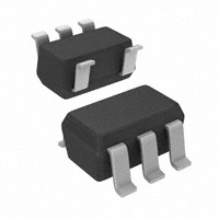
DBV PACKAGE
(TOP VIEW)
50-mA Low-Dropout Regulator
Fixed Output Voltage Options: 5 V, 3.8 V,
3.3 V, 3.2 V, and 3 V
Dropout Typically 120 mV at 50 mA
Thermal Protection
Less Than 1-µA Quiescent Current in
Shutdown
–40°C to 125°C Operating Junction
Temperature Range
5-Pin SOT-23 Package
ESD Protection Verified to 1.5 kV Human
Body Model (HBM) per MIL-STD-883C
EN
GND
IN
3
2
1
4
5
NC
OUT
NC – No internal connection
description
The TPS760xx is a 50 mA, low dropout (LDO) voltage regulator designed specifically for battery-powered
applications. A proprietary BiCMOS fabrication process allows the TPS760xx to provide outstanding
performance in all specifications critical to battery-powered operation.
The TPS760xx is available in a space-saving SOT–23 package and operates over a junction temperature range
of –40°C to 125°C.
AVAILABLE OPTIONS
TJ
VOLTAGE
– 40°C to 125°C
PART NUMBER
SYMBOL
3V
TPS76030DBVR
PAGI
3.2 V
TPS76032DBVR
PAOI
TPS76033DBVR
PAHI
3.3 V
PACKAGE
SOT-23
3.8 V
TPS76038DBVR
PAJI
5V
TPS76050DBVR
PANI
NOTE: The DBV package is available taped and reeled only.
functional block diagram
†
CS
IN
OUT
EN
Current
Limit
Vref +
Thermal
Sense
GND
† Current sense
Please be aware that an important notice concerning availability, standard warranty, and use in critical applications of
Texas Instruments semiconductor products and disclaimers thereto appears at the end of this data sheet.
Copyright 2001, Texas Instruments Incorporated
PRODUCTION DATA information is current as of publication date.
Products conform to specifications per the terms of Texas Instruments
standard warranty. Production processing does not necessarily include
testing of all parameters.
POST OFFICE BOX 655303
• DALLAS, TEXAS 75265
1
�TPS76030, TPS76032, TPS76033, TPS76038, TPS76050
LOW-POWER 50-mA LOW-DROPOUT LINEAR REGULATORS
SLVS144D – JULY 1998 – REVISED MAY 2001
Terminal Functions
TERMINAL
NAME
NO.
EN
3
GND
2
IN
1
NC
4
OUT
5
I/O
I
DESCRIPTION
Enable input
Ground
I
Input voltage
No connection
O
Regulated output voltage
absolute maximum ratings over operating free-air temperature range (unless otherwise noted)†
Input voltage range, VI‡ . . . . . . . . . . . . . . . . . . . . . . . . . . . . . . . . . . . . . . . . . . . . . . . . . . . . . . . . . . . . . . . . . . . –0.3 V to 16 V
Voltage range at EN . . . . . . . . . . . . . . . . . . . . . . . . . . . . . . . . . . . . . . . . . . . . . . . . . . . . . . . . . . . . . . . . . –0.3 V to VI + 0.3 V
Peak output current . . . . . . . . . . . . . . . . . . . . . . . . . . . . . . . . . . . . . . . . . . . . . . . . . . . . . . . . . . . . . . . internally limited
Continuous total dissipation . . . . . . . . . . . . . . . . . . . . . . . . . . . . . . . . . . . . . . . . . . . . See Dissipation Rating Table
Operating junction temperature range, TJ . . . . . . . . . . . . . . . . . . . . . . . . . . . . . . . . . . . . . . . . . . . –40°C to 150°C
Storage temperature range, Tstg . . . . . . . . . . . . . . . . . . . . . . . . . . . . . . . . . . . . . . . . . . . . . . . . . . . . . . . . . –65°C to 150°C
ESD rating, HBM . . . . . . . . . . . . . . . . . . . . . . . . . . . . . . . . . . . . . . . . . . . . . . . . . . . . . . . . . . . . . . . . . . . . . . . . . 1.5 kV
† Stresses beyond those listed under “absolute maximum ratings” may cause permanent damage to the device. These are stress ratings only, and
functional operation of the device at these or any other conditions beyond those indicated under “recommended operating conditions” is not
implied. Exposure to absolute-maximum-rated conditions for extended periods may affect device reliability.
‡ All voltages are with respect to device GND pin.
DISSIPATION RATING TABLE
BOARD
PACKAGE
RθJC
RθJA
DERATING FACTOR
ABOVE TA = 25°C
TA ≤ 25°C
POWER RATING
TA = 70°C
POWER RATING
TA = 85°C
POWER RATING
Low K§
High K¶
DBV
65.8 °C/W
259 °C/W
3.9 mW/°C
386 mW
212 mW
154 mW
DBV
65.8 °C/W
180 °C/W
5.6 mW/°C
555 mW
305 mW
222 mW
§ The JEDEC Low K (1s) board design used to derive this data was a 3 inch x 3 inch, two layer board with 2 ounce copper traces on top of the board.
¶ The JEDEC High K (2s2p) board design used to derive this data was a 3 inch x 3 inch, multilayer board with 1 ounce internal power and ground
planes and 2 ounce copper traces on top and bottom of the board.
recommended operating conditions
MIN
Input voltage, VI
MAX
3.2
16
TPS76032
3.4
16
TPS76033
3.5
16
TPS76038
4
16
TPS76050
5.2
16
Continuous output current, IO
Operating junction temperature, TJ
2
NOM
TPS76030
POST OFFICE BOX 655303
• DALLAS, TEXAS 75265
UNIT
V
0
50
mA
– 40
125
°C
�TPS76030, TPS76032, TPS76033, TPS76038, TPS76050
LOW-POWER 50-mA LOW-DROPOUT LINEAR REGULATORS
SLVS144D – JULY 1998 – REVISED MAY 2001
electrical characteristics over recommended operating free-air temperature range,
VI = VO(nom) + 1 V, IO = 1 mA, EN = VI, Co = 2.2 µF (unless otherwise noted)
PARAMETER
TEST CONDITIONS
TPS76030
TPS76032
TJ = 25°C
TJ = 25°C,
1 mA < IO < 50 mA
Output voltage
TPS76033
2.91
3.07
TJ = 25°C
TJ = 25°C,
3.16
1 mA < IO < 50 mA
TJ = 25°C
TJ = 25°C,
1 mA < IO < 50 mA
TJ = 25°C
TJ = 25°C,
Standby current
Vn
3.3
3.34
3.2
3.4
TJ = 25°C
TJ = 25°C,
3.84
3.7
3.9
5
5.05
4.89
5.1
1
IO = 0 mA,
IO = 0 mA
TJ = 25°C
IO = 1 mA,
IO = 1 mA
TJ = 25°C
100
IO = 10 mA,
IO = 10 mA
TJ = 25°C
190
215
IO = 50 mA,
IO = 50 mA
TJ = 25°C
850
1100
TPS76030
4 V < VI < 16,
10
4.2 V < VI < 16,
3
10
TPS76033
4.3 V < VI < 16,
IO = 1 mA
IO = 1 mA
IO = 1 mA
3
TPS76032
3
10
TPS76038
4.8 V < VI < 16,
10
6 V < VI < 16,
IO = 1 mA
IO = 1 mA
3
TPS76050
3
10
130
µA
1200
Ripple rejection
f = 1 kHz,
Co = 10 µF,
IO = 0 mA TJ = 25°C
IO = 0 mA
Co = 10 µF, TJ = 25°C
TJ = 25°C
63
1
mV
µVrms
190
dB
3
5
IO = 1 mA,
IO = 1 mA
TJ = 25°C
IO = 10 mA,
IO = 10 mA
TJ = 25°C
40
60
IO = 50 mA
IO = 50 mA
TJ = 25°C
120
150
7
10
15
mV
90
180
100
High level enable input
125
135
2
EN = 0 V
–1
EN = VI
• DALLAS, TEXAS 75265
mA
V
Low level enable input
POST OFFICE BOX 655303
µA
260
BW = 300 Hz to 50 kHz,
Input current (EN)
V
115
170
Peak output current/current limit
II
V
130
Output noise voltage
Dropout voltage
V
5.05
4.91
90
V
3.84
3.73
4.95
1 mA < IO < 50 mA
3.8
V
3.34
3.23
EN = 0 V
Quiescent current (GND current)
Input regulation
3.24
3.3
UNIT
3.24
3.1
3.76
1 mA < IO < 50 mA
3.2
3.13
3.26
1 mA < IO < 50 mA
II(standby)
3.04
1 mA < IO < 50 mA
1 mA < IO < 50 mA
TPS76050
MAX
3
3.04
1 mA < IO < 50 mA
TPS76038
TYP
2.92
1 mA < IO < 50 mA
VO
MIN
2.96
0.8
V
0
1
µA
2.5
5
µA
3
�TPS76030, TPS76032, TPS76033, TPS76038, TPS76050
LOW-POWER 50-mA LOW-DROPOUT LINEAR REGULATORS
SLVS144D – JULY 1998 – REVISED MAY 2001
Table of Graphs
FIGURE
VO
Zo
VDO
4
Output voltage
vs Output current
1, 2, 3
vs Free-air temperature
4, 5, 6
Ground current
vs Free-air temperature
7, 8, 9
Output noise
vs Frequency
Output impedance
vs Frequency
11
Dropout voltage
vs Free-air temperature
12
10
Line transient response
13, 15
Load transient response
14, 16
POST OFFICE BOX 655303
• DALLAS, TEXAS 75265
�TPS76030, TPS76032, TPS76033, TPS76038, TPS76050
LOW-POWER 50-mA LOW-DROPOUT LINEAR REGULATORS
SLVS144D – JULY 1998 – REVISED MAY 2001
TYPICAL CHARACTERISTICS
TPS76030
TPS76033
OUTPUT VOLTAGE
vs
OUTPUT CURRENT
OUTPUT VOLTAGE
vs
OUTPUT CURRENT
3.305
3.005
VI = 4 V
TA = 25°C
3.3
VO – Output Voltage – V
3
VO – Output Voltage – V
VI = 4.3 V
TA = 25°C
2.995
2.99
2.985
2.98
3.295
3.29
3.285
3.28
3.275
3.27
2.975
0
10
20
30
40
50
0
60
10
20
Figure 1
50
40
60
Figure 2
TPS76050
TPS76030
OUTPUT VOLTAGE
vs
OUTPUT CURRENT
OUTPUT VOLTAGE
vs
FREE-AIR TEMPERATURE
3.15
5.02
VI = 4 V
VI = 6 V
TA = 25°C
3.1
VO – Output Voltage – V
5.01
VO – Output Voltage – V
30
IO – Output Current – mA
IO – Output Current – mA
5
4.99
4.98
4.97
3.05
IO = 1 mA
3
IO = 50 mA
2.95
2.9
4.96
0
10
20
30
40
50
60
2.85
–55 –35
–15
5
25
45
65
85
105
125
TA – Free-Air Temperature – °C
IO – Output Current – mA
Figure 3
Figure 4
POST OFFICE BOX 655303
• DALLAS, TEXAS 75265
5
�TPS76030, TPS76032, TPS76033, TPS76038, TPS76050
LOW-POWER 50-mA LOW-DROPOUT LINEAR REGULATORS
SLVS144D – JULY 1998 – REVISED MAY 2001
TYPICAL CHARACTERISTICS
TPS76033
TPS76050
OUTPUT VOLTAGE
vs
FREE-AIR TEMPERATURE
OUTPUT VOLTAGE
vs
FREE-AIR TEMPERATURE
5.1
3.35
VI = 6 V
VI = 4.3 V
5.08
IO = 1 mA
5.06
VO – Output Voltage – V
VO – Output Voltage – V
3.3
IO = 50 mA
3.25
3.2
5.04
5.02
IO = 1 mA
5
4.98
IO = 50 mA
4.96
4.94
4.92
3.15
–55 –35
–15
5
25
45
65
85
105
4.9
–55 –35
125
TA – Free-Air Temperature – °C
–15
Figure 5
85
TPS76033
GROUND CURRENT
vs
FREE-AIR TEMPERATURE
105
125
105
125
10000
VI = 4.3 V
IO = 50 mA
Ground Current – µ A
Ground Current – µ A
65
TPS76030
IO = 10 mA
IO = 1 mA
10
–55 –35
–15
1000
IO = 50 mA
IO = 10 mA
100
IO = 1 mA
IO = 0 mA
IO = 0 mA
5
25
45
65
85
105
125
10
–55 –35
–15
5
25
Figure 7
Figure 8
POST OFFICE BOX 655303
45
65
85
TA – Free-Air Temperature – °C
TA – Free-Air Temperature – °C
6
45
GROUND CURRENT
vs
FREE-AIR TEMPERATURE
VI = 4 V
100
25
Figure 6
10000
1000
5
TA – Free-Air Temperature – °C
• DALLAS, TEXAS 75265
�TPS76030, TPS76032, TPS76033, TPS76038, TPS76050
LOW-POWER 50-mA LOW-DROPOUT LINEAR REGULATORS
SLVS144D – JULY 1998 – REVISED MAY 2001
TYPICAL CHARACTERISTICS
OUTPUT NOISE
vs
FREQUENCY
TPS76050
GROUND CURRENT
vs
FREE-AIR TEMPERATURE
10 µV ǸHz
10000
VI = 6 V
10 µV ǸHz
Output Noise
Ground Current – µ A
IO = 50 mA
1000
IO = 10 mA
100
IO = 1 mA
1 µV ǸHz
CL = 10 µF
IO = 50 mA
100 nV ǸHz
IO = 0 mA
10
–55 –35
–15
CL = 2.2 µF
IO = 50 mA
CL = 2.2 µF
IO = 1 mA
CL = 10 µF
IO = 1 mA
5
25
45
85
65
105
125
10 nV ǸHz
250
1k
10k
100k
f – Frequency – Hz
TA – Free-Air Temperature – °C
Figure 9
Figure 10
TPS76030
OUTPUT IMPEDANCE
vs
FREQUENCY
DROPOUT VOLTAGE
vs
FREE-AIR TEMPERATURE
150
CL = 2.2 µF:
IO = 1 mA
IO = 10 mA
IO = 50 mA
1
VI = EN = 2.9 V
50 mA
125
VDO – Dropout Voltage – mV
Zo – Output Impedance – Ω
10
CL = 10 µF:
IO = 1 mA
IO = 10 mA
CL = 10 µF
IO = 50 mA
100
75
10 mA
50
25
0.1
0.01
0.1
1
10
100
1000
0
–55 –35
0 mA
–15
5
25
1 mA
45
65
85
105
125
TA – Free-Air Temperature – °C
f – Frequency – kHz
Figure 11
Figure 12
POST OFFICE BOX 655303
• DALLAS, TEXAS 75265
7
�TPS76030, TPS76032, TPS76033, TPS76038, TPS76050
LOW-POWER 50-mA LOW-DROPOUT LINEAR REGULATORS
SLVS144D – JULY 1998 – REVISED MAY 2001
TYPICAL CHARACTERISTICS
TPS76033
LINE TRANSIENT RESPONSE
TPS76033
LOAD TRANSIENT RESPONSE
100
∆ VO – Change in
Output Voltage – mV
20
0
–20
–30
I O – Output Current – mA
VI – Input Voltage – V
∆ VO – Change in
Output Voltage – mV
40
6
5
4
CO = 2.2 µF
3
0
20
40
60
CO = 2.2 µF
50
0
–50
–100
60
40
20
0
0
80 100 120 140 160 180 200
t – Time – µs
20
40
60
Figure 14
Figure 13
TPS76050
LINE TRANSIENT RESPONSE
∆ VO – Change in
Output Voltage – mV
∆ VO – Change in
Output Voltage – mV
40
20
0
I O – Output Current – mA
–20
VI – Input Voltage – V
TPS76050
LOAD TRANSIENT RESPONSE
150
60
8
7
6
CO = 2.2 µF
5
0
50
100 150 200 250 300 350 400 450 500
t – Time – µs
100
50
0
CO = 2.2 µF
–50
60
40
20
0
0
20
40
60
80 100 120 140 160 180 200
t – Time – µs
Figure 16
Figure 15
8
80 100 120 140 160 180 200
t – Time – µs
POST OFFICE BOX 655303
• DALLAS, TEXAS 75265
�TPS76030, TPS76032, TPS76033, TPS76038, TPS76050
LOW-POWER 50-mA LOW-DROPOUT LINEAR REGULATORS
SLVS144D – JULY 1998 – REVISED MAY 2001
APPLICATION INFORMATION
1
IN
CI = 1 µF
EN
5
TPS760xx
OUT
Co = 2.2 µF
3
2
GND
Figure 17. TPS760xx Typical Application
over current protection
The over current protection circuit forces the TPS760xx into a constant current output mode when the load is
excessive or the output is shorted to ground. Normal operation resumes when the fault condition is removed.
An overload or short circuit may also activate the over temperature protection if the fault condition persists.
over temperature protection
The thermal protection system shuts the TPS760xx down when the junction temperature exceeds 160°C. The
device recovers and operates normally when the temperature drops below 155°C.
input capacitor
A 0.047 µF or larger ceramic decoupling capacitor with short leads connected between IN and GND is
recommended. The decoupling capacitor may be omitted if there is a 1 µF or larger electrolytic capacitor
connected between IN and GND and located reasonably close to the TPS760xx. However, the small ceramic
device is desirable even when the larger capacitor is present, if there is a lot of high frequency noise present
in the system.
output capacitor
Like all low dropout regulators, the TPS760xx requires an output capacitor connected between OUT and GND
to stabilize the internal control loop. The minimum recommended capacitance value is 2.2 µF and the ESR
(equivalent series resistance) must be between 0.1 Ω and 20 Ω. Capacitor values of 2.5-µF or larger are
acceptable, provided the ESR is less than 20 Ω. Solid tantalum electrolytic, aluminum electrolytic, and multilayer
ceramic capacitors are all suitable, provided they meet the requirements described above. Most of the
commercially available 2.2-µF surface-mount solid-tantalum capacitors, including devices from Sprague,
Kemet, and Nichicon, meet the ESR requirements stated above. Multilayer ceramic capacitors should have
minimum values of 2.5 µF over the full operating temperature range of the equipment.
enable (EN)
A logic zero on the enable input shuts the TPS760xx off and reduces the supply current to less than 1 µA. Pulling
the enable input high causes normal operation to resume. If the enable feature is not used, EN should be
connected to IN to keep the regulator on all of the time. The EN input must not be left floating.
reverse current path
The power transistor used in the TPS760xx has an inherent diode connected between IN and OUT as shown
in the functional block diagram. This diode conducts current from the OUT terminal to the IN terminal whenever
IN is lower than OUT by a diode drop. This condition does not damage the TPS760xx, provided the current is
limited to 100 mA.
POST OFFICE BOX 655303
• DALLAS, TEXAS 75265
9
�PACKAGE OPTION ADDENDUM
www.ti.com
13-Aug-2021
PACKAGING INFORMATION
Orderable Device
Status
(1)
Package Type Package Pins Package
Drawing
Qty
Eco Plan
(2)
Lead finish/
Ball material
MSL Peak Temp
Op Temp (°C)
Device Marking
(3)
(4/5)
(6)
TPS76030DBVR
ACTIVE
SOT-23
DBV
5
3000
RoHS & Green
NIPDAU
Level-1-260C-UNLIM
-40 to 125
PAGI
TPS76030DBVT
ACTIVE
SOT-23
DBV
5
250
RoHS & Green
NIPDAU
Level-1-260C-UNLIM
-40 to 125
PAGI
TPS76032DBVR
ACTIVE
SOT-23
DBV
5
3000
RoHS & Green
NIPDAU
Level-1-260C-UNLIM
-40 to 125
PAOI
TPS76033DBVR
ACTIVE
SOT-23
DBV
5
3000
RoHS & Green
NIPDAU
Level-1-260C-UNLIM
-40 to 125
PAHI
TPS76033DBVT
ACTIVE
SOT-23
DBV
5
250
RoHS & Green
NIPDAU
Level-1-260C-UNLIM
-40 to 125
PAHI
TPS76038DBVR
ACTIVE
SOT-23
DBV
5
3000
RoHS & Green
NIPDAU
Level-1-260C-UNLIM
-40 to 125
PAJI
TPS76038DBVT
ACTIVE
SOT-23
DBV
5
250
RoHS & Green
NIPDAU
Level-1-260C-UNLIM
-40 to 125
PAJI
TPS76050DBVR
ACTIVE
SOT-23
DBV
5
3000
RoHS & Green
NIPDAU
Level-1-260C-UNLIM
-40 to 125
PANI
TPS76050DBVRG4
ACTIVE
SOT-23
DBV
5
3000
RoHS & Green
NIPDAU
Level-1-260C-UNLIM
-40 to 125
PANI
TPS76050DBVT
ACTIVE
SOT-23
DBV
5
250
RoHS & Green
NIPDAU
Level-1-260C-UNLIM
-40 to 125
PANI
(1)
The marketing status values are defined as follows:
ACTIVE: Product device recommended for new designs.
LIFEBUY: TI has announced that the device will be discontinued, and a lifetime-buy period is in effect.
NRND: Not recommended for new designs. Device is in production to support existing customers, but TI does not recommend using this part in a new design.
PREVIEW: Device has been announced but is not in production. Samples may or may not be available.
OBSOLETE: TI has discontinued the production of the device.
(2)
RoHS: TI defines "RoHS" to mean semiconductor products that are compliant with the current EU RoHS requirements for all 10 RoHS substances, including the requirement that RoHS substance
do not exceed 0.1% by weight in homogeneous materials. Where designed to be soldered at high temperatures, "RoHS" products are suitable for use in specified lead-free processes. TI may
reference these types of products as "Pb-Free".
RoHS Exempt: TI defines "RoHS Exempt" to mean products that contain lead but are compliant with EU RoHS pursuant to a specific EU RoHS exemption.
Green: TI defines "Green" to mean the content of Chlorine (Cl) and Bromine (Br) based flame retardants meet JS709B low halogen requirements of


 工商网监
湘ICP备2023018690号
工商网监
湘ICP备2023018690号
