TPS767D3xx
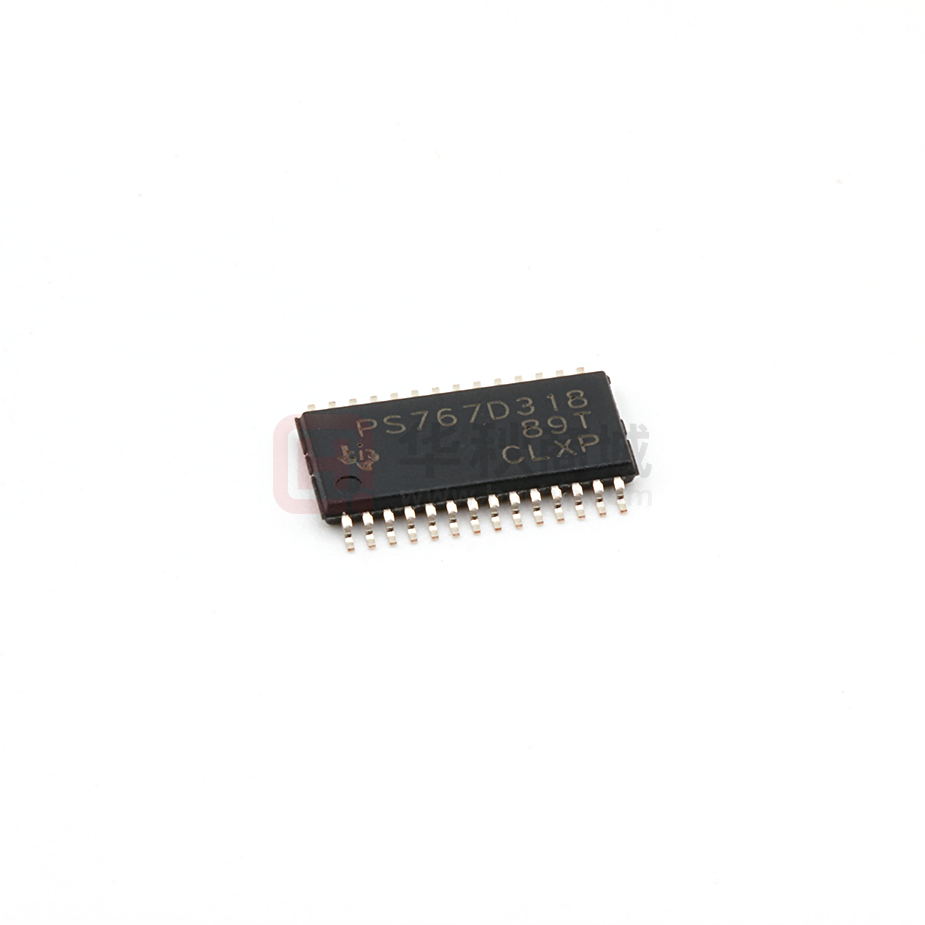
www.ti.com......................................................................................................................................................... SLVS209H – JULY 1999 – REVISED AUGUST 2008
DUAL-OUTPUT LOW-DROPOUT VOLTAGE REGULATORS
FEATURES
1
• Dual Output Voltages for Split-Supply
Applications
• Output Current Range of 0mA to 1.0A per
Regulator
• 3.3V/2.5V, 3.3V/1.8V, and 3.3V/Adjustable
Output
• Fast-Transient Response
• 2% Tolerance Over Load and Temperature
• Dropout Voltage Typically 350mV at 1A
• Ultra-low 85µA Typical Quiescent Current
• 1µA Quiescent Current During Shutdown
• Dual Open-Drain Power-On Reset with 200ms
Delay for Each Regulator
• 28-Pin PowerPAD™ TSSOP Package
• Thermal Shutdown Protection for Each
Regulator
Because the PMOS device behaves as a low-value
resistor, the dropout voltage is very low (350mV
typically at an output current of 1A for the
TPS767D325) and is directly proportional to the
output current. Additionally, since the PMOS pass
element is a voltage-driven device, the quiescent
current is very low and independent of output loading
(typically 85µA over the full range of output current,
0mA to 1A). These two key specifications yield a
significant improvement in operating life for
battery-powered systems. This LDO family also
features a sleep mode; applying a TTL high signal to
EN (enable) shuts down the regulator, reducing the
quiescent current to 1µA at TJ = +25°C.
DESCRIPTION
The TPS767D3xx is offered in 1.8V, 2.5V, and 3.3V
fixed-voltage versions and in an adjustable version
(programmable over the range of 1.5V to 5.5V).
Output voltage tolerance is specified as a maximum
of 2% over line, load, and temperature ranges. The
TPS767D3xx family is available in a 28-pin PWP
TSSOP package. They operate over a junction
temperature range of –40°C to +125°C.
23
The TPS767D3xx family of dual voltage regulators
offers fast transient response, low dropout voltages
and dual outputs in a compact package and
incorporating stability with 10µF low ESR output
capacitors.
The TPS767D3xx family of dual voltage regulators is
designed primarily for DSP applications. These
devices can be used in any mixed-output voltage
application, with each regulator supporting up to 1A.
Dual active-low reset signals allow resetting of
core-logic and I/O separately.
The RESET output of the TPS767D3xx initiates a
reset in microcomputer and microprocessor systems
in the event of an undervoltage condition. An internal
comparator in the TPS767D3xx monitors the output
voltage of the regulator to detect an undervoltage
condition on the regulated output voltage.
LINE TRANSIENT RESPONSE
VOUT = 3.3V
CL = 10mF
5.3
TA = 25°C
4.3
10
0
10
VDO - Dropout Voltage - mV
DVOUT - Change in
Output Voltage - mV
VIN - Input Voltage - V
PWP PACKAGE
(TOP VIEW)
10
3
10
1
IOUT = 10mA
10
10
10
20 40 60 80 100 120 140 160 180 200
t - Time - ms
IOUT = 1A
2
-1
-10
0
DROPOUT VOLTAGE
vs FREE-AIR TEMPERATURE
-2
VOUT = 3.3V
COUT = 10mF
IOUT = 0
-60 -40 -20 0 20 40 60 80 100 120 140
TA - Free-Air Temperature - °C
NC
1
28
1RESET
NC
2
27
NC
1GND
3
26
NC
1EN
4
25
1FB/NC
1IN
5
24
1OUT
1IN
6
23
1OUT
NC
7
22
2RESET
NC
8
21
NC
2GND
9
20
NC
2EN
10
19
NC
2IN
11
18
2OUT
2IN
12
17
2OUT
NC
13
16
NC
NC
14
15
NC
NC = No internal connection
1
2
3
Please be aware that an important notice concerning availability, standard warranty, and use in critical applications of Texas
Instruments semiconductor products and disclaimers thereto appears at the end of this data sheet.
PowerPAD is a trademark of Texas Instruments.
All other trademarks are the property of their respective owners.
PRODUCTION DATA information is current as of publication date.
Products conform to specifications per the terms of the Texas
Instruments standard warranty. Production processing does not
necessarily include testing of all parameters.
Copyright © 1999–2008, Texas Instruments Incorporated
�TPS767D3xx
SLVS209H – JULY 1999 – REVISED AUGUST 2008......................................................................................................................................................... www.ti.com
This integrated circuit can be damaged by ESD. Texas Instruments recommends that all integrated circuits be handled with
appropriate precautions. Failure to observe proper handling and installation procedures can cause damage.
ESD damage can range from subtle performance degradation to complete device failure. Precision integrated circuits may be more
susceptible to damage because very small parametric changes could cause the device not to meet its published specifications.
AVAILABLE OPTIONS (1)
(1)
DEVICE
REGULATOR 1 VOUT (V)
REGULATOR 2 VOUT (V)
TPS767D301
Adjustable (1.5V – 5.5V)
3.3V
TPS767D318
1.8V
3.3V
TPS767D325
2.5V
3.3V
For the most current specifications and package information see the Package Option Addendum at the end of this document, or see the
TI web site at www.ti.com.
ABSOLUTE MAXIMUM RATINGS (1)
Over operating temperature range (unless otherwise noted).
TPS767D3xx
UNIT
Input voltage range, V1IN, V2IN (2)
–0.3 to +13.5
V
Enable voltage range, V1EN, V2EN
–0.3 to VIN + 0.3
V
Output voltage range, V1OUT, V2OUT
–0.3 to +7.0
V
RESET voltage range, V1RESET, V2RESET
–0.3 to +16.5
V
Peak output current
Internally limited
ESD rating, HBM
2
kV
Continuous total power dissipation
See Dissipation Ratings table
Operating junction temperature range, TJ
–40 to +125
°C
Storage temperature range, Tstg
–65 to +150
°C
(1)
(2)
Stresses beyond those listed under absolute maximum ratings may cause permanent damage to the device. These are stress ratings
only, and functional operation of the device at these or any other conditions beyond those indicated under recommended operating
conditions is not implied. Exposure to absolute-maximum-rated conditions for extended periods may affect device reliability.
All voltage values are with respect to network terminal ground.
POWER DISSIPATION RATINGS
PACKAGE
PWP (1)
(1)
2
AIR FLOW
(CFM)
TA ≤ +25°C
POWER RATING
DERATING FACTOR
ABOVE ta = +25°C
TA = +70°C
POWER RATING
TA = +85°C
POWER RATING
0
3.58 W
35.8 mW/°C
1.97 W
1.43 W
250
5.07 W
50.7 mW/°C
2.79 W
2.03 W
This parameter is measured with the recommended copper heat sink pattern on a 4-layer PCB, 1oz. copper on 4-in × 4-in ground layer.
For more information, refer to TI technical brief literature number SLMA002.
Submit Documentation Feedback
Copyright © 1999–2008, Texas Instruments Incorporated
�TPS767D3xx
www.ti.com......................................................................................................................................................... SLVS209H – JULY 1999 – REVISED AUGUST 2008
ELECTRICAL CHARACTERISTICS
Over operating temperature range (TJ = –40°C to +125°C), VIN = VOUT(nom) + 1V, IOUT = 1mA, VEN = 0V, and
COUT = 10µF, unless otherwise noted. Adjustable channels are set to VOUT = 3.3V. Typical values are at TJ = 25°C.
PARAMETER
TEST CONDITIONS
MIN
TYP
MAX
UNIT
Input voltage range, V1IN, V2IN (1)
2.7
10
V
Adjustable VOUT range, V1OUT, V2OUT
1.5
5.5
V
Accuracy, adjustable VOUT channels (1)
VOUT + 1V ≤ VIN ≤ 5.5V;
10 µA ≤ IOUT ≤ 1A
–2.0
+2.0
%
Accuracy, fixed VOUT channels (1)
VOUT + 1V ≤ VIN ≤ 10V;
10 µA ≤ IOUT ≤ 1A
–2.0
+2.0
%
ΔVOUT%/ΔVIN
Line regulation (1)
VOUT + 1.0V ≤ VIN ≤ 10V
ΔVOUT%/ΔIOUT
Load regulation
10 µA ≤ IOUT ≤ 1A
VDO
Dropout voltage (2)
(VIN = VOUT (nom) – 0.1V)
VOUT = 3.3V, IOUT = 1A
350
ICL
Output current limit, per LDO
VOUT = 0V, TJ = +25°C
1.7
2
A
IGND
Ground pin current, per LDO
10µA ≤ IOUT ≤ 1A
85
125
µA
ISHDN
Standby current, per LDO
2.7V ≤ VIN ≤ 10V, VEN = VIN
1
10
µA
IFB
FB current input (Adjustable)
VFB = 1.5V
2
nA
PSRR
Power-supply ripple rejection
f = 1kHz, COUT = 10µF
60
dB
VN
Output noise voltage
BW = 200Hz to 100kHz, VOUT = 1.8V,
IC = 1A, COUT = 10µF
55
µVRMS
VEN(HI)
High-level enable input voltage
TJ = +25°C
VEN(LO)
Low-level enable input voltage
TJ = +25°C
VIN
VOUT
IEN
Input current
Reset
–1
VOUT decreasing, TJ = +25°C
Hysteresis voltage
Measured at VOUT
Output low voltage
VI = 2.7V, TJ = +25°C,
IOUT(RESET)= 1mA
Leakage current
V(RESET) = 7V, TJ = +25°C
RESET time-out delay
TJ = +25°C
TSD
Thermal shutdown temperature
TJ
Operating junction temperature
(1)
(2)
VEN = VIN, TJ = +25°C
Trip threshold voltage
mV
575
0
1
1
1.1
92
98
µA
%VOUT
%VOUT
0.15
0.4
1
µA
200
400
ms
150
–40
V
V
0.5
100
mV
V
0.8
–1
IOUT(RESET) = 300µA
%/V
3
2.0
VEN = 0V, TJ = +25°C
Minimum input voltage for valid
RESET
0.01
V
°C
+125
°C
Minimum VIN = VOUT + VDO or 2.7V, whichever is greater.
Dropout voltage (VDO) is not measured for channels with VOUT(nom) < 2.8V since minimum VIN = 2.7V.
Copyright © 1999–2008, Texas Instruments Incorporated
Submit Documentation Feedback
3
�TPS767D3xx
SLVS209H – JULY 1999 – REVISED AUGUST 2008......................................................................................................................................................... www.ti.com
FUNCTIONAL BLOCK DIAGRAM—Fixed Voltage Version (one regulator channel)
IN
EN
RESET
OUT
200ms Delay
VREF =
1.1834V
R1
R2
GND
FUNCTIONAL BLOCK DIAGRAM—Adjustable Version (one regulator channel)
IN
EN
RESET
OUT
200ms Delay
VREF =
1.1834V
R1
FB/NC
R2
GND
4
Submit Documentation Feedback
External to
the device
Copyright © 1999–2008, Texas Instruments Incorporated
�TPS767D3xx
www.ti.com......................................................................................................................................................... SLVS209H – JULY 1999 – REVISED AUGUST 2008
PWP PACKAGE
(TOP VIEW)
NC
1
28
1RESET
NC
2
27
NC
1GND
3
26
NC
1EN
4
25
1FB/NC
1IN
5
24
1OUT
1IN
6
23
1OUT
NC
7
22
2RESET
NC
8
21
NC
2GND
9
20
NC
2EN
10
19
NC
2IN
11
18
2OUT
2IN
12
17
2OUT
NC
13
16
NC
NC
14
15
NC
NC = No internal connection
TERMINAL FUNCTIONS
TERMINAL
DESCRIPTION
NAME
NO.
1GND
3
Regulator #1 ground
1EN
4
Regulator #1 enable
1IN
5, 6
Regulator #1 input supply voltage
2GND
9
Regulator #2 ground
2EN
10
Regulator #2 enable
2IN
11, 12
Regulator #2 input supply voltage
2OUT
17, 18
Regulator #2 output voltage
2RESET
22
Regulator #2 reset signal
1OUT
23, 24
Regulator #1 output voltage
1FB/NC
25
Regulator #1 output voltage feedback for adjustable output; no connection for fixed output
1RESET
28
Regulator #1 reset signal
NC
1, 2, 7, 8,
13–16, 19,
20, 21, 26,
27
No internal connection
Copyright © 1999–2008, Texas Instruments Incorporated
Submit Documentation Feedback
5
�TPS767D3xx
SLVS209H – JULY 1999 – REVISED AUGUST 2008......................................................................................................................................................... www.ti.com
TPS767D3xx
VIN
5
28
IN
6
250kW
IN
OUT
C1
0.1mF
50V
RESET
RESET
4
OUT
EN
24
VOUT
23
+ COUT
10mF
GND
3
Figure 1. Typical Application Circuit (Fixed Versions) for Single Channel
TIMING DIAGRAM
VIN
VRES
(1)
VRES
t
VOUT
(2)
VIT+
VIT+
Threshold
Voltage
VIN-
(2)
Less than 5% of
the output voltage
VIN-
t
RESET
Output
200ms
Delay
200ms
Delay
Output
Undefined
Output
Undefined
t
6
(1)
VRES is the minimum input voltage for a valid RESET.
(2)
VIT —Trip voltage is typically 5% lower than the output voltage (95% VOUT).
Submit Documentation Feedback
Copyright © 1999–2008, Texas Instruments Incorporated
�TPS767D3xx
www.ti.com......................................................................................................................................................... SLVS209H – JULY 1999 – REVISED AUGUST 2008
TYPICAL CHARACTERISTICS
OUTPUT VOLTAGE
vs
OUTPUT CURRENT
3.2835
OUTPUT VOLTAGE
vs
OUTPUT CURRENT
1.7965
VOUT = 3.3V
VIN = 4.3V
TA = +25°C
3.2830
OUTPUT VOLTAGE
vs
OUTPUT CURRENT
2.4960
VOUT = 1.8V
VIN = 2.8V
TA =+25°C
VOUT = 2.5V
VIN = 3.5V
TA = +25°C
2.4955
3.2820
3.2815
3.2810
VOUT - Output Voltage - V
VOUT - Output Voltage - V
VOUT - Output Voltage - V
1.7960
3.2825
1.7955
1.7950
2.4950
2.4945
2.4940
2.4935
2.4930
1.7945
3.2805
2.4925
3.2800
0
0.2 0.3
0.1
0.4
0.5
0.6 0.7
0.8
0.9
1.7940
1
2.4920
0
0.1
0.2 0.3
IOUT - Output Current - A
0
0.1 0.2 0.3
0.4 0.5
0.6 0.7
0.8 0.9
Figure 4.
OUTPUT VOLTAGE
vs
FREE-AIR TEMPERATURE
OUTPUT VOLTAGE
vs
FREE-AIR TEMPERATURE
OUTPUT VOLTAGE
vs
FREE-AIR TEMPERATURE
1.815
VOUT = 3.3V
VIN = 4.3V
2.515
VOUT = 1.8V
VIN = 2.8V
IOUT = 1mA
3.28
3.27
1.805
IOUT = 1A
1.800
IOUT = 1mA
1.795
VOUT - Output Voltage - V
IOUT = 1A
1.790
3.25
−60 −40 −20
0
20
40
60
80
VOUT = 2.5V
VIN = 3.5V
2.505
2.500
IOUT = 1A
2.495
IOUT = 1mA
2.490
2.485
1.785
−60 −40 −20
100 120 140
0
20
40
60
80
2.480
−60 −40
100 120 140
TA - Free-Air Temperature - °C
TA - Free-Air Temperature - °C
1
2.510
1.810
VOUT - Output Voltage - V
VOUT - Output Voltage - V
1
Figure 3.
3.26
−20 0
20 40
60
80
TA - Free-Air Temperature - °C
100 120
Figure 5.
Figure 6.
Figure 7.
GROUND CURRENT
vs
FREE-AIR TEMPERATURE
GROUND CURRENT
vs
FREE-AIR TEMPERATURE
POWER SUPPLY RIPPLE REJECTION
vs
FREQUENCY
96
VOUT = 3.3V
VIN = 4.3V
94
88
92
86
90
84
82
IOUT = 1mA
IOUT = 1A
78
Ground Current - mA
Ground Current - mA
0.9
Figure 2.
3.29
80
0.8
IOUT - Output Current - A
3.30
90
0.6 0.7
IOUT - Output Current - A
3.31
92
0.5
90
VOUT = 1.8V
VIN = 2.8V
IOUT = 1mA
88
86
IOUT = 500mA
84
82
80
IOUT = 500mA
76
78
74
76
72
−60 −40 −20
0
20
40
60
80
100 120 140
TA - Free-Air Temperature - °C
Figure 8.
Copyright © 1999–2008, Texas Instruments Incorporated
IOUT = 1A
74
−60 −40 −20
0
20
40
60
80
100 120 140
TA - Free-Air Temperature - °C
Figure 9.
PSRR - Power-Supply Ripple Rejection - dB
3.32
0.4
VOUT = 3.3V
VIN = 4.3V
COUT = 10mF
IOUT = 1A
TA = +25°C
80
70
60
50
40
30
20
10
0
−10
10
100
1k
10k
100k
1M
f - Frequency - Hz
Figure 10.
Submit Documentation Feedback
7
�TPS767D3xx
SLVS209H – JULY 1999 – REVISED AUGUST 2008......................................................................................................................................................... www.ti.com
TYPICAL CHARACTERISTICS (continued)
OUTPUT SPECTRAL NOISE DENSITY
vs
FREQUENCY
0
IOUT = 1A
10−7
10−8
102
103
104
IOUT = 1A
102
IOUT = 1mA
10−1
102
103
104
f - Frequency - Hz
Figure 11.
0
−20
20
40
60
−50
VOUT = 3.3V
COUT = 10mF
TA = +25°C
5.3
4.3
−100
1
0.5
0
20
40
60
10
0
−10
80 100 120 140 160 180 200
0
20
40
t - Time - ms
60
80 100 120 140 160 180 200
t - Time - ms
Figure 16.
LOAD TRANSIENT RESPONSE
OUTPUT VOLTAGE
vs
TIME (AT START-UP)
DROPOUT VOLTAGE
vs
INPUT VOLTAGE
0
−50
900
4
IOUT = 1A
800
3
VDO - Dropout Voltage - mV
VO - Output Voltage - V
DVO - Change in
Output Voltage - mV
2
1
0
Enable Pulse - V
IO - Output Current - A
80 100 120 140
Figure 15.
−100
1
0.5
0
20
40
60
Figure 17.
Submit Documentation Feedback
700
600
500
0
TA = +125°C
TA = +25°C
400
300
200
TA = -40°C
100
0
80 100 120 140 160 180 200
t - Time - ms
8
60
LINE TRANSIENT RESPONSE
0
0
40
Figure 14.
VOUT = 3.3V
COUT = 100mF
TA = +25°C
0
20
Figure 13.
VOUT = 1.8V
VIN = 2.8V
COUT = 100mF
TA = +25°C
50
80 100 120 140 160 180 200
t - Time - ms
100
50
0
TA - Free-Air Temperature - °C
DVO - Change in
Output Voltage - mV
DVO - Change in
Output Voltage - mV
IO - Output Current - A
VI - Input Voltage - V
DVO - Change in
Output Voltage - mV
20
0
−60 −40 −20
106
LOAD TRANSIENT RESPONSE
100
VOUT = 1.8V
IOUT = 10mA
COUT = 10mF
TA = +25°C
105
IOUT = 0
VOUT = 3.3V
COUT = 10mF
Figure 12.
LINE TRANSIENT RESPONSE
2.8
IOUT = 10mA
100
10−2
f - Frequency - Hz
3.8
101
10−1
IOUT = 1A
10−2
101
105
103
VIN = 4.3V
COUT = 10mF
TA = 25°C
VI - Input Voltage - V
IOUT = 7mA
10−6
DROPOUT VOLTAGE
vs
FREE-AIR TEMPERATURE
VDO - Dropout Voltage - mV
VIN = 4.3V
COUT = 10mF
TA = +25°C
ZOUT - Output Impedance - W
Vn - Output Spectral Noise Density - V/ÖHz
10−5
OUTPUT IMPEDANCE
vs
FREQUENCY
0
20
40
60
80 100 120 140 160 180 200
t - Time - ms
Figure 18.
2.5
3
3.5
4
4.5
5
VI - Input Voltage - V
Figure 19.
Copyright © 1999–2008, Texas Instruments Incorporated
�TPS767D3xx
www.ti.com......................................................................................................................................................... SLVS209H – JULY 1999 – REVISED AUGUST 2008
VIN
IN
To Load
OUT
+
EN
COUT
RL
GND
ESR
Figure 20. Test Circuit for Typical Regions of Stability (Figure 21 through Figure 24)
(Fixed Output Options)
Equivalent series resistance (ESR) refers to the total series resistance, including the ESR of the capacitor, any
resistance added externally, and PWB trace resistance to COUT.
TYPICAL REGION OF STABILITY
ESR vs OUTPUT CURRENT
TYPICAL REGION OF STABILITY
ESR vs OUTPUT CURRENT
10
10
ESR - Equivalent Series Resistance - W
ESR - Equivalent Series Resistance - W
Region of Instability
Region of Instability
1
VOUT = 3.3V
COUT = 4.7mF
VIN = 4.3V
TA = +25°C
Region of Stability
0.1
Region of Instability
VOUT = 3.3V
COUT = 4.7mF
VIN = 4.3V
TA = +125°C
Region of Stability
0.1
Region of Instability
0.01
0.01
0
200
400
600
800
0
1000
200
400
600
800
IOUT - Output Current - mA
IOUT - Output Current - mA
Figure 21.
Figure 22.
TYPICAL REGION OF STABILITY
ESR vs OUTPUT CURRENT
TYPICAL REGION OF STABILITY
ESR vs OUTPUT CURRENT
1000
10
ESR - Equivalent Series Resistance - W
10
ESR - Equivalent Series Resistance - W
1
Region of Instability
1
VOUT = 3.3V
COUT = 22mF
VIN = 4.3V
TA = +25°C
Region of Stability
0.1
Region of Instability
Region of Instability
1
VOUT = 3.3V
COUT = 22mF
VIN = 4.3V
TA = +125°C
Region of Stability
0.1
Region of Instability
0.01
0.01
0
200
400
600
IOUT - Output Current - mA
Figure 23.
Copyright © 1999–2008, Texas Instruments Incorporated
800
1000
0
200
400
600
800
1000
IOUT - Output Current - mA
Figure 24.
Submit Documentation Feedback
9
�TPS767D3xx
SLVS209H – JULY 1999 – REVISED AUGUST 2008......................................................................................................................................................... www.ti.com
APPLICATION INFORMATION
The features of the TPS767D3xx family (low-dropout voltage, ultra low quiescent current, power-saving shutdown
mode, and a supply-voltage supervisor) and the power-dissipation properties of the TSSOP PowerPAD package
have enabled the integration of the dual LDO regulator with high output current for use in DSP and other multiple
voltage applications. Figure 25 shows a typical dual-voltage DSP application.
U1
TPS767D325
R1
100kW
1
NC
1RESET
28
2
NC
NC
27
3
1GND
NC
26
4
1EN
1FB/NC
25
5
1IN
1OUT
24
6
1IN
1OUT
23
7
NC
2RESET
22
8
NC
NC
21
9
2GND
NC
20
10
2EN
NC
19
11
2IN
2OUT
18
12
2IN
2OUT
17
13
NC
NC
16
14
NC
NC
15
R2
100kW
PG
RESET to DSP
5V
DSP
C0
1m F
2.5V
+ C3
33mF
3.3V
C1
1mF
VCORE
VI/O
C2
33mF
GND
GND
Figure 25. Dual-Voltage DSP Application
DSP power requirements include very high transient currents that must be considered in the initial design. This
design uses higher-valued output capacitors to handle the large transient currents.
DEVICE OPERATION
The TPS767D3xx features very low quiescent current, which remain virtually constant even with varying loads.
Conventional LDO regulators use a pnp pass element, the base current of which is directly proportional to the
load current through the regulator (IB = IC/β). Close examination of the data sheets reveals that these devices are
typically specified under near no-load conditions; actual operating currents are much higher as evidenced by
typical quiescent current versus load current curves. The TPS767D3xx uses a PMOS transistor to pass current;
because the gate of the PMOS is voltage driven, operating current is low and invariable over the full load range.
The TPS767D3xx specifications reflect actual performance under load condition.
Another pitfall associated with the pnp pass element is its tendency to saturate when the device goes into
dropout. The resulting drop in β forces an increase in IB to maintain the load. During power-up, this translates to
large start-up currents. Systems with limited supply current may fail to start up. In battery-powered systems, it
means rapid battery discharge when the voltage decays below the minimum required for regulation. The
TPS767D3xx quiescent current remains low even when the regulator drops out, eliminating both problems.
10
Submit Documentation Feedback
Copyright © 1999–2008, Texas Instruments Incorporated
�TPS767D3xx
www.ti.com......................................................................................................................................................... SLVS209H – JULY 1999 – REVISED AUGUST 2008
The TPS767D3xx family also features a shutdown mode that places the output in the high-impedance state
(essentially equal to the feedback-divider resistance) and reduces quiescent current to under 2µA. If the
shutdown feature is not used, EN should be tied to ground. Response to an enable transition is quick; regulated
output voltage is typically re-established in 120µs.
MINIMUM LOAD REQUIREMENTS
The TPS767D3xx family is stable even at zero load; no minimum load is required for operation.
FB-PIN CONNECTION (ADJUSTABLE VERSION ONLY)
The FB pin is an input pin to sense the output voltage and close the loop for the adjustable option. The output
voltage is sensed through a resistor divider network as is shown in Figure 26 to close the loop. Normally, this
connection should be as short as possible; however, the connection can be made near a critical circuit to
improve performance at that point. Internally, FB connects to a high-impedance, wide-bandwidth amplifier and
noise pickup feeds through to the regulator output. Routing the FB connection to minimize/avoid noise pickup is
essential. In fixed output options, this pin is not connected.
EXTERNAL CAPACITOR REQUIREMENTS
An input capacitor is not required; however, a ceramic bypass capacitor (0.047pF to 0.1µF) improves load
transient response and noise rejection when the TPS767D3xx is located more than a few inches from the power
supply. A higher-capacitance electrolytic capacitor may be necessary if large (hundreds of milliamps) load
transients with fast rise times are anticipated.
Like all low dropout regulators, the TPS767D3xx requires an output capacitor connected between OUT and GND
to stabilize the internal control loop. The minimum recommended capacitance value is 10µF and the ESR
(equivalent series resistance) must be between 60mΩ and 1.5Ω. Capacitor values of 10µF or larger are
acceptable, provided the ESR is less than 1.5Ω. Solid tantalum electrolytic, aluminum electrolytic, and multilayer
ceramic capacitors are all suitable, provided they meet the requirements described previously.
When necessary to achieve low height requirements along with high output current and/or high ceramic load
capacitance, several higher ESR capacitors can be used in parallel to meet the previous guidelines.
PROGRAMMING THE TPS767D301 ADJUSTABLE LDO REGULATOR
The output voltage of the TPS767D301 adjustable regulator is programmed using an external resistor divider as
shown in Figure 26. The output voltage is calculated using:
V OUT + VREF
ǒ1) RR Ǔ
1
2
(1)
Resistors R1 and R2 should be chosen for approximately 40µA divider current. Lower-value resistors can be used
but offer no inherent advantage and waste more power. Higher values should be avoided as leakage currents at
FB increase the output voltage error.
Copyright © 1999–2008, Texas Instruments Incorporated
Submit Documentation Feedback
11
�TPS767D3xx
SLVS209H – JULY 1999 – REVISED AUGUST 2008......................................................................................................................................................... www.ti.com
The recommended design procedure is to choose R2 = 30.1 kΩ to set the divider current at 40µA and then
calculate R1 using:
R1 +
ǒVV
OUT
REF
Ǔ
R2
*1
(2)
TPS767D301
VIN
IN
RESET Output
RESET
250kW
0.1mF
VOUT
OUT
> 2.7V
R1
EN
< 0.5V
FB/NC
GND
R2
+ COUT
10mF
OUTPUT VOLTAGE
PROGRAMMING GUIDE
OUTPUT
VOLTAGE
R1
R2
UNIT
2.5V
33.2
30.1
kW
3.3V
53.6
30.1
kW
3.6V
61.9
30.1
kW
4.75V
90.8
30.1
kW
Figure 26. TPS767D301 Adjustable LDO Regulator Programming
RESET INDICATOR
The TPS767D3xx features a RESET output that can be used to monitor the status of the regulator. The internal
comparator monitors the output voltage: when the output drops to 95% (typical) of its regulated value, the
RESET output transistor turns on, taking the signal low. The open-drain output requires a pullup resistor. If not
used, it can be left floating. RESET can be used to drive power-on reset circuitry or as a low-battery indicator.
REGULATOR PROTECTION
The TPS767D3xx PMOS-pass transistor has a built-in back-gate diode that safely conducts reverse currents
when the input voltage drops below the output voltage (for example, during power-down). Current is conducted
from the output to the input and is not internally limited. When extended reverse voltage is anticipated, external
limiting may be appropriate.
The TPS767D3xx also features internal current limiting and thermal protection. During normal operation, the
TPS767D3xx limits output current to approximately 1.7A. When current limiting engages, the output voltage
scales back linearly until the overcurrent condition ends. While current limiting is designed to prevent gross
device failure, care should be taken not to exceed the power dissipation ratings of the package. If the
temperature of the device exceeds +150°C (typ), thermal-protection circuitry shuts it down. Once the device has
cooled below +130°C (typ), regulator operation resumes.
12
Submit Documentation Feedback
Copyright © 1999–2008, Texas Instruments Incorporated
�TPS767D3xx
www.ti.com......................................................................................................................................................... SLVS209H – JULY 1999 – REVISED AUGUST 2008
POWER DISSIPATION AND JUNCTION TEMPERATURE
Specified regulator operation is assured to a junction temperature of +125°C; the maximum junction temperature
should be restricted to +125°C under normal operating conditions. This restriction limits the power dissipation the
regulator can handle in any given application. To ensure the junction temperature is within acceptable limits,
calculate the maximum allowable dissipation, PDmax, and the actual dissipation, PD, which must be less than or
equal to PDmax.
The maximum-power-dissipation limit is determined using the following equation:
PD max +
T J max *T A
RQJA
(3)
Where:
• TJmax is the maximum allowable junction temperature.
• RθJA is the thermal resistance junction-to-ambient for the package, that is, 28°C/W for the 28-terminal PWP
with no airflow.
• TA is the ambient temperature.
The regulator dissipation is calculated using:
PD + ǒ V IN*VOUT Ǔ
I OUT
(4)
Power dissipation resulting from quiescent current is negligible. Excessive power dissipation will trigger the
thermal protection circuit.
Copyright © 1999–2008, Texas Instruments Incorporated
Submit Documentation Feedback
13
�TPS767D3xx
SLVS209H – JULY 1999 – REVISED AUGUST 2008......................................................................................................................................................... www.ti.com
Revision History
Changes from Revision F (February 2008) to Revision G ............................................................................................. Page
•
14
Changed Corrected symbol for FB current in Electrical Characteristics................................................................................ 3
Submit Documentation Feedback
Copyright © 1999–2008, Texas Instruments Incorporated
�PACKAGE OPTION ADDENDUM
www.ti.com
10-Dec-2020
PACKAGING INFORMATION
Orderable Device
Status
(1)
Package Type Package Pins Package
Drawing
Qty
Eco Plan
(2)
Lead finish/
Ball material
MSL Peak Temp
Op Temp (°C)
Device Marking
(3)
(4/5)
(6)
TPS767D301PWP
ACTIVE
HTSSOP
PWP
28
50
RoHS & Green
NIPDAU
Level-2-260C-1 YEAR
-40 to 125
PS767D301
TPS767D301PWPG4
ACTIVE
HTSSOP
PWP
28
50
RoHS & Green
NIPDAU
Level-2-260C-1 YEAR
-40 to 125
PS767D301
TPS767D301PWPR
ACTIVE
HTSSOP
PWP
28
2000
RoHS & Green
NIPDAU
Level-2-260C-1 YEAR
-40 to 125
PS767D301
TPS767D301PWPRG4
ACTIVE
HTSSOP
PWP
28
2000
RoHS & Green
NIPDAU
Level-2-260C-1 YEAR
-40 to 125
PS767D301
TPS767D318PWP
ACTIVE
HTSSOP
PWP
28
50
RoHS & Green
NIPDAU
Level-2-260C-1 YEAR
-40 to 125
PS767D318
TPS767D318PWPG4
ACTIVE
HTSSOP
PWP
28
50
RoHS & Green
NIPDAU
Level-2-260C-1 YEAR
-40 to 125
PS767D318
TPS767D318PWPR
ACTIVE
HTSSOP
PWP
28
2000
RoHS & Green
NIPDAU
Level-2-260C-1 YEAR
-40 to 125
PS767D318
TPS767D325PWP
ACTIVE
HTSSOP
PWP
28
50
RoHS & Green
NIPDAU
Level-2-260C-1 YEAR
-40 to 125
PS767D325
TPS767D325PWPG4
ACTIVE
HTSSOP
PWP
28
50
RoHS & Green
NIPDAU
Level-2-260C-1 YEAR
-40 to 125
PS767D325
TPS767D325PWPR
ACTIVE
HTSSOP
PWP
28
2000
RoHS & Green
NIPDAU
Level-2-260C-1 YEAR
-40 to 125
PS767D325
(1)
The marketing status values are defined as follows:
ACTIVE: Product device recommended for new designs.
LIFEBUY: TI has announced that the device will be discontinued, and a lifetime-buy period is in effect.
NRND: Not recommended for new designs. Device is in production to support existing customers, but TI does not recommend using this part in a new design.
PREVIEW: Device has been announced but is not in production. Samples may or may not be available.
OBSOLETE: TI has discontinued the production of the device.
(2)
RoHS: TI defines "RoHS" to mean semiconductor products that are compliant with the current EU RoHS requirements for all 10 RoHS substances, including the requirement that RoHS substance
do not exceed 0.1% by weight in homogeneous materials. Where designed to be soldered at high temperatures, "RoHS" products are suitable for use in specified lead-free processes. TI may
reference these types of products as "Pb-Free".
RoHS Exempt: TI defines "RoHS Exempt" to mean products that contain lead but are compliant with EU RoHS pursuant to a specific EU RoHS exemption.
Green: TI defines "Green" to mean the content of Chlorine (Cl) and Bromine (Br) based flame retardants meet JS709B low halogen requirements of