Sample &
Buy
Product
Folder
Support &
Community
Tools &
Software
Technical
Documents
TPS768-Q1
SGLS155B – FEBRUARY 2003 – REVISED NOVEMBER 2016
TPS768xx-Q1 Fast-Transient-Response 1-A Low-Dropout Voltage Regulators
1 Features
3 Description
•
•
This device is designed to have a fast transient
response and be stable with 10 μF capacitors. This
combination provides high performance at a
reasonable cost.
1
•
•
•
•
•
•
•
•
•
Qualified for Automotive Applications
AEC-Q100 Qualified With the Following Results:
– Device Temperature Grade 1: –40°C to 125°C
Ambient Operating Temperature Range
– Device HBM ESD Classification Level H2
– Device CDM ESD Classification Level C4B
1-A Low-Dropout (LDO) Voltage Regulator
Available in 1.8-V, 2.5-V, 3.3-V, and 5-V FixedOutput and an Adjustable Version
Dropout Voltage Down to 230 mV at 1 A
(TPS76850-Q1)
Ultralow 85-μA Typical Quiescent Current
Fast Transient Response
2% Tolerance Over Specified Conditions for
Fixed-Output Versions
Open-Drain Power Good (See TPS767xx-Q1 for
Power-On Reset With 200-ms Delay Option)
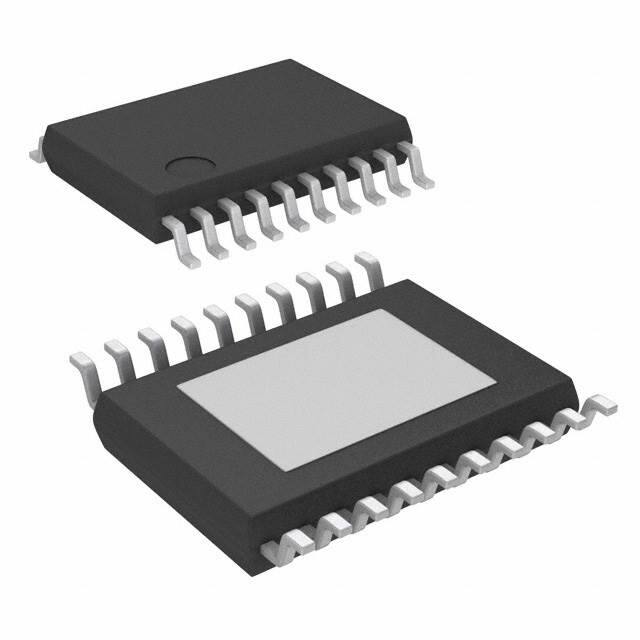
20-Pin TSSOP (PWP) Package
Thermal Shutdown Protection
2 Applications
•
•
•
•
Automotive
Power Train
Cluster
ADAS
Because the PMOS device behaves as a low-value
resistor, the dropout voltage is very low (typically
230 mV at an output current of 1 A for the TPS76850Q1) and is directly proportional to the output current.
Additionally, because the PMOS pass element is a
voltage-driven device, the quiescent current is very
low and independent of output loading (typically
85 μA over the full range of output current, 0 mA to
1 A). These two key specifications yield a significant
improvement in operating life for battery-powered
systems. This LDO family also features a shutdown
mode; applying a TTL high signal to the enable (EN)
input shuts down the regulator, reducing the
quiescent current to less than 1 μA at TJ = 25°C.
Power good (PG) is an active-high output, which can
be used to implement a power-on reset or a lowbattery indicator.
The TPS768xx-Q1 is offered in 1.8-V, 2.5-V, 3.3-V,
and 5-V fixed-voltage versions and in an adjustable
version (programmable over the range of 1.2 V to 5.5
V). Output voltage tolerance is specified as a
maximum of 2% over line, load, and temperature
ranges. The TPS768xx-Q1 family is available in a 20pin PWP package.
Device Information(1)
PART NUMBER
TPS768xx-Q1
PACKAGE
HTSSOP (20)
BODY SIZE (NOM)
6.50 mm × 4.40 mm
(1) For all available packages, see the orderable addendum at
the end of the data sheet.
Typical Application Circuit
Load Transient Response
TPS768xx-Q1
C1
0.1 mF
PG
IN
IN
250 kW
OUT
5
PG
EN
OUT
14
VO
13
Co = 10 mF
TA = 25°C
50
0
−50
−100
+
GND
D VO − Change in
Output Voltage − mV
7
16
Co
10 mF
3
Copyright © 2016, Texas Instruments Incorporated
I O − Output Current − A
VI
6
100
1
0.5
0
0
100 200 300 400 500 600 700 800 900 1000
t − Time − ms
1
An IMPORTANT NOTICE at the end of this data sheet addresses availability, warranty, changes, use in safety-critical applications,
intellectual property matters and other important disclaimers. PRODUCTION DATA.
�TPS768-Q1
SGLS155B – FEBRUARY 2003 – REVISED NOVEMBER 2016
www.ti.com
Table of Contents
1
2
3
4
5
6
7
8
Features ..................................................................
Applications ...........................................................
Description .............................................................
Revision History.....................................................
Pin Configuration and Functions .........................
Specifications.........................................................
1
1
1
2
3
4
6.1
6.2
6.3
6.4
6.5
6.6
4
4
4
4
5
6
Absolute Maximum Ratings .....................................
ESD Ratings..............................................................
Recommended Operating Conditions.......................
Thermal Information ..................................................
Electrical Characteristics...........................................
Typical Characteristics ..............................................
Parameter Measurement Information .................. 9
Detailed Description ............................................ 10
8.1 Overview ................................................................. 10
8.2 Functional Block Diagrams ..................................... 10
8.3 Feature Description................................................. 11
8.4 Device Functional Modes........................................ 11
9
Application and Implementation ........................ 13
9.1 Application Information............................................ 13
9.2 Typical Application ................................................. 13
10 Power Supply Recommendations ..................... 15
11 Layout................................................................... 15
11.1 Layout Guidelines ................................................. 15
11.2 Layout Example .................................................... 16
11.3 Power Dissipation and Junction Temperature ...... 16
12 Device and Documentation Support ................. 17
12.1
12.2
12.3
12.4
12.5
Receiving Notification of Documentation Updates
Community Resources..........................................
Trademarks ...........................................................
Electrostatic Discharge Caution ............................
Glossary ................................................................
17
17
17
17
17
13 Mechanical, Packaging, and Orderable
Information ........................................................... 17
4 Revision History
NOTE: Page numbers for previous revisions may differ from page numbers in the current version.
Changes from Revision A (September 2008) to Revision B
Page
•
Added AEC-Q100 qualifications ............................................................................................................................................ 1
•
Deleted Ordering Information table ........................................................................................................................................ 1
•
Added Applications section, ESD Ratings table, Thermal Information table, Feature Description section, Device
Functional Modes, Application and Implementation section, Power Supply Recommendations section, Layout
section, Device and Documentation Support section, and Mechanical, Packaging, and Orderable Information section. ..... 1
•
Deleted 1.5-V, 2.7-V, and 3-V versions throughout the data sheet........................................................................................ 1
•
Changed Pin Configuration and Functions section ................................................................................................................ 3
•
Deleted the "Continuous total power dissipation" row from the Absolute Maximum Ratings table........................................ 4
•
Changed TJ to TA in the Recommended Operating Conditions table..................................................................................... 4
•
Deleted Dissipation Ratings table .......................................................................................................................................... 4
2
Submit Documentation Feedback
Copyright © 2003–2016, Texas Instruments Incorporated
Product Folder Links: TPS768-Q1
�TPS768-Q1
www.ti.com
SGLS155B – FEBRUARY 2003 – REVISED NOVEMBER 2016
5 Pin Configuration and Functions
PWP PowerPAD™ Package
20-Pin HTSSOP With Exposed Thermal Pad
Top View
GND/HSINK
1
20
GND/HSINK
GND/HSINK
2
19
GND/HSINK
GND
3
18
NC
NC
4
17
NC
EN
5
16
PG
15
FB/NC
Thermal
IN
6
IN
7
14
OUT
NC
8
13
OUT
GND/HSINK
9
12
GND/HSINK
GND/HSINK
10
11
GND/HSINK
Pad
Not to scale
NC – No internal connection
Pin Functions
PIN
NAME
NO.
EN
5
FB/NC
GND
GND/HSINK
I/O
DESCRIPTION
I
Enable input
15
I
Feedback input voltage for adjustable device (no connect for fixed options)
3
—
1, 2, 9, 10, 11,
12, 19, 20
—
LDO ground
Ground and heatsink
IN
6, 7
I
NC
4, 8, 17, 18
—
No connect
13, 14
O
Regulated output voltage
OUT
Input
PG
16
O
Power-good output
NC
17
—
No connect
Thermal pad
—
—
Solder the thermal pad to the board.
Submit Documentation Feedback
Copyright © 2003–2016, Texas Instruments Incorporated
Product Folder Links: TPS768-Q1
3
�TPS768-Q1
SGLS155B – FEBRUARY 2003 – REVISED NOVEMBER 2016
www.ti.com
6 Specifications
6.1 Absolute Maximum Ratings (1)
over operating ambient temperature range (unless otherwise noted)
Input voltage, VI
(2)
Voltage at EN
MIN
MAX
UNIT
–0.3
13.5
V
–0.3
VI + 0.3
V
16.5
V
Maximum PG voltage
Peak output current
Internally limited
Output voltage, VO (OUT, FB)
7
V
Operating junction temperature, TJ
–40
150
°C
Storage temperature, Tstg
–65
150
°C
(1)
(2)
Stresses beyond those listed under Absolute Maximum Ratings may cause permanent damage to the device. These are stress ratings
only, and do not imply functional operation of the device at these or any other conditions beyond those indicated under Recommended
Operating Conditions. Exposure to absolute-maximum-rated conditions for extended periods may affect device reliability.
All voltage values are with respect to network terminal ground.
6.2 ESD Ratings
VALUE
Human-body model (HBM), per AEC Q100-002
Electrostatic
discharge
V(ESD)
(1)
(1)
Charged-device model (CDM), per AEC Q100-011
UNIT
±2000
All pins
±500
Corner pins (1, 4, 5, and 8)
±750
V
AEC Q100-002 indicates that HBM stressing shall be in accordance with the ANSI/ESDA/JEDEC JS-001 specification.
6.3 Recommended Operating Conditions
MIN
MAX
UNIT
VI
Input voltage
(1)
2.7
10
V
VO
Voltage at OUT
1.2
5.5
V
IO
Output current (2)
0
1
A
TA
Operating ambient temperature (2)
–40
125
°C
(1)
(2)
To calculate the minimum input voltage for the maximum output current, use the following equation: VI(min) = VO(max) + V(DO,max_load),
where V(DO,max_load) is the dropout voltage at maximum load.
Continuous current and operating junction temperature are limited by internal protection circuitry, but it is not recommended that the
device operate under conditions beyond those specified in this table for extended periods of time.
6.4 Thermal Information
TPS768xx-Q1
THERMAL METRIC
(1)
PWP (HTSSOP)
UNIT
20 PINS
RθJA
Junction-to-ambient thermal resistance
39.5
°C/W
RθJC(top)
Junction-to-case (top) thermal resistance
25.8
°C/W
RθJB
Junction-to-board thermal resistance
22.1
°C/W
ψJT
Junction-to-top characterization parameter
0.8
°C/W
ψJB
Junction-to-board characterization parameter
21.9
°C/W
RθJC(bot)
Junction-to-case (bottom) thermal resistance
1.7
°C/W
(1)
4
For more information about traditional and new thermal metrics, see the Semiconductor and IC Package Thermal Metrics application
report, SPRA953.
Submit Documentation Feedback
Copyright © 2003–2016, Texas Instruments Incorporated
Product Folder Links: TPS768-Q1
�TPS768-Q1
www.ti.com
SGLS155B – FEBRUARY 2003 – REVISED NOVEMBER 2016
6.5 Electrical Characteristics
over recommended operating ambient temperature range, VI = VO(typ) + 1 V, IO = 1 mA, EN = 0 V, CO = 10 μF (unless
otherwise noted)
PARAMETER
TEST CONDITIONS
MIN
TYP
TJ = 25°C
Output voltage
(10-μA to 1-A load) (1)
TPS76801-Q1
5.5 V ≥ VO ≥ 1.5 V
TPS76818-Q1
2.8 V < VIN < 10 V
TPS76825-Q1
3.5 V < VIN < 10 V
TPS76833-Q1
4.3 V < VIN < 10 V
TPS76850-Q1
6 V < VIN < 10 V
TJ = –40°C to 125°C
0.98 ×
VO
Output voltage line regulation (ΔVO / VO)
(1) (2)
TJ = 25°C
1.8
TJ = –40°C to 125°C
1.764
1.836
TJ = 25°C
2.5
TJ = –40°C to 125°C
2.45
TPS76818-Q1
Output current limit
TJ = 25°C
3.3
TJ = –40°C to 125°C
3.234
3.366
TJ = 25°C
5
TJ = –40°C to 125°C
4.9
5.1
85
TJ = –40°C to 125°C IO = 1 A, TJ = –40°C to
125°C
125
TJ = 25°C VO + 1 V < VI ≤ 10 V, TJ = 25°C
%/V
3
mV
55
μVrms
TJ = 25°C BW = 200 Hz to 100 kHz, CO = 10 μF,
IC = 1 A, TJ = 25°C
VO = 0 V
1.7
FB input current
TPS76801-Q1
TJ = 25°C
10
VFB = 1.5 V
2
V
Low-level enable input voltage
PG
0.9
TJ = 25°C f = 1 kHz, CO = 10 μF, TJ = 25°C
60
Minimum input voltage for valid PG
IO(PG) = 300 μA
1.1
Trip threshold voltage
VO decreasing
Hysteresis voltage
Measured at VO
Output low voltage
VI = 2.7 V, IO(PG) = 1 mA
Leakage current
V(PG) = 5 V
EN input current
(3)
EN = VI
–1
TJ = 25°C
IO = 1 A
TPS76850-Q1
(1)
(2)
(3)
V
0.5
0
%VO
V
1
μA
1
μA
350
575
TJ = 25°C
230
TJ = –40°C to 125°C
Minimum IN operating voltage is 2.7 V or VO(typ) + 1 V, whichever is greater. Maximum IN voltage 10 V.
ǒV Imax*2.7VǓ
Line Reg. (mV) + (% ń V)
VO
1000
100
If VO ≤ 1.8 V then VI(max) = 10 V, VI(min) = 2.7 V:
ǒV Imax*ǒVO)1VǓǓ
Line Reg. (mV) + (% ń V)
VO
100
If VO ≥ 2.5 V then VI(max) = 10 V, VI(min) = VO + 1 V:
IN voltage equals VO(typ) – 100 mV.
mV
380
1000
Submit Documentation Feedback
Product Folder Links: TPS768-Q1
%VO
0.4
1
TJ = –40°C to 125°C
Copyright © 2003–2016, Texas Instruments Incorporated
V
dB
98
0.15
–1
TPS76833-Q1
Dropout voltage
92
EN = 0 V
μA
nA
1.7
(1)
A
°C
1
TJ = –40°C to 125°C
High-level enable input voltage
Power-supply ripple rejection
2
150
EN = VI,
2.7 V < VI < 10 V
μA
0.01
Thermal shutdown junction temperature
Standby current
V
2.55
Load regulation
Output noise voltage
UNIT
1.02 ×
VO
TJ = 25°C 10 μA < IO < 1 A, TJ = 25°C
Quiescent current (GND current), EN = 0 V (1)
MAX
VO
5
�TPS768-Q1
SGLS155B – FEBRUARY 2003 – REVISED NOVEMBER 2016
www.ti.com
6.6 Typical Characteristics
3.2835
2.4960
VI = 4.3 V
TA = 25°C
VI = 3.5 V
TA = 25°C
2.4955
2.4950
3.2825
VO − Output Voltage − V
VO − Output Voltage − V
3.2830
3.2820
3.2815
3.2810
3.2805
2.4945
2.4940
2.4935
2.4930
2.4925
3.2800
0
0.1
0.2 0.3
0.4
0.5
0.8
0.6 0.7
0.9
2.4920
1
0
0.1 0.2 0.3
IO − Output Current − A
Figure 1. TPS76833-Q1 Output Voltage vs Output Current
1
VI = 3.5 V
3.31
2.510
3.30
2.505
VO − Output Voltage − V
VO − Output Voltage − V
0.8 0.9
2.515
VI = 4.3 V
3.29
IO = 1 A
IO = 1 mA
3.28
3.27
2.500
IO = 1 A
2.495
IO = 1 mA
2.490
2.485
3.26
3.25
−60 −40 −20
0
20
40
60
80
2.480
−60 −40
100 120 140
−20
0
20
40
60
80
100 120
TA − Free-Air Temperature − °C
TA − Free-Air Temperature − °C
Figure 3. TPS76833-Q1 Output Voltage vs Ambient
Temperature
Figure 4. TPS76825-Q1 Output Voltage vs Ambient
Temperature
92
PSRR − Power Supply Ripple Rejection − dB
90
90
VI = 4.3 V
88
Ground Current − m A
0.6 0.7
Figure 2. TPS76825-Q1 Output Voltage vs Output Current
3.32
86
84
82
IO = 1 mA
80
IO = 1 A
78
IO = 500 mA
76
74
72
−60 −40 −20
0
20
40
60
80
100 120 140
VI = 4.3 V
Co = 10 mF
IO = 1 A
TA = 25°C
80
70
60
50
40
30
20
10
0
−10
10
100
1k
10k
100k
1M
f − Frequency − Hz
TA − Free-Air Temperature − °C
Figure 5. TPS76833-Q1 Ground Current vs Ambient
Temperature
6
0.4 0.5
IO − Output Current − A
Figure 6. TPS76833-Q1 Power-Supply Ripple Rejection vs
Frequency
Submit Documentation Feedback
Copyright © 2003–2016, Texas Instruments Incorporated
Product Folder Links: TPS768-Q1
�TPS768-Q1
www.ti.com
SGLS155B – FEBRUARY 2003 – REVISED NOVEMBER 2016
Typical Characteristics (continued)
4
VI = 4.3 V
Co = 10 mF
TA = 25°C
IO = 1 A
TA = 25°C
VI − Input Voltage (Min) − V
Output Spectral Noise Density − m V Hz
10−5
IO = 7 mA
10−6
IO = 1 A
10−7
10−8
102
103
104
TA = 125°C
3
TA = −40°C
2.7
2
1.5
105
1.75
2
Figure 7. TPS76833-Q1 Output Spectral Noise Density vs
Frequency
2.5
3.25
3.5
IO = 1 A
VDO − Dropout Voltage − mV
102
IO = 1 mA
10−1
IO = 1 A
101
IO = 10 mA
100
10−1
IO = 0
Co = 10 mF
10−2
101
103
104
f − Frequency − kHz
102
105
10−2
−60 −40 −20
106
0
20
40
60
80 100 120 140
TA − Free-Air Temperature − °C
Figure 9. TPS76833-Q1 Output Impedance vs Frequency
Figure 10. TPS76833-Q1 Dropout Voltage vs Ambient
Temperature
100
D VO − Change in
Output Voltage − mV
VI − Input Voltage − V
3
103
VI = 4.3 V
Co = 10 mF
TA = 25°C
Co = 10 mF
TA = 25°C
5.3
I O − Output Current − A
4.3
D VO − Change in
Output Voltage − mV
2.75
Figure 8. Input Voltage (Min.) vs Output Voltage
0
Zo − Output Impedance − W
2.25
VO − Output Voltage − V
f − Frequency − Hz
10
0
−10
0
20
40
60
0
−50
−100
1
0.5
0
80 100 120 140 160 180 200
t − Time − ms
Figure 11. TPS76833-Q1 Line Transient Response
Co = 10 mF
TA = 25°C
50
0
100 200 300 400 500 600 700 800 900 1000
t − Time − ms
Figure 12. TPS76833-Q1 Load Transient Response
Submit Documentation Feedback
Copyright © 2003–2016, Texas Instruments Incorporated
Product Folder Links: TPS768-Q1
7
�TPS768-Q1
SGLS155B – FEBRUARY 2003 – REVISED NOVEMBER 2016
www.ti.com
Typical Characteristics (continued)
900
IO = 1 A
Co = 10 mF
IO = 1 A
TA = 25°C
3
800
VDO − Dropout Voltage − mV
VO− Output Voltage − V
4
2
1
Enable Pulse − V
0
700
600
500
TA = 125°C
TA = 25°C
400
300
200
TA = −40°C
100
0
0
0.1
0.2 0.3
0.4 0.5 0.6 0.7 0.8
t − Time − ms
0.9
2.5
1
Figure 13. TPS76833-Q1 Output Voltage vs Time (at StartUp)
ESR − Equivalent Series Resistance − W
ESR − Equivalent Series Resistance − W
4.5
5
10
Region of Instability
1
VO = 3.3 V
Co = 4.7 mF
VI = 4.3 V
TA = 25°C
Region of Stability
0.1
Region of Instability
Region of Instability
1
VO = 3.3 V
Co = 4.7mF
VI = 4.3 V
TJ = 125°C
Region of Stability
0.1
Region of Instability
0.01
0.01
0
200
400
600
800
1000
0
200
400
600
800
1000
IO − Output Current − mA
IO − Output Current − mA
Figure 15. Typical Region of Stability Equivalent Series
Resistance (4) vs Output Current
Figure 16. Typical Region of Stability Equivalent Series
Resistance (4) vs Output Current
10
Region of Instability
ESR − Equivalent Series Resistance − W
ESR − Equivalent Series Resistance − W
10
1
VO = 3.3 V
Co = 22 mF
VI = 4.3 V
TA = 25°C
Region of Stability
0.1
Region of Instability
0.01
Region of Instability
1
VO = 3.3 V
Co = 22 mF
VI = 4.3 V
TJ = 125°C
Region of Stability
0.1
Region of Instability
0.01
0
8
4
3.5
VI − Input Voltage − V
Figure 14. TPS76801-Q1 Dropout Voltage vs Input Voltage
10
(4)
3
200
400
600
800
1000
0
200
400
600
800
1000
IO − Output Current − mA
IO − Output Current − mA
Figure 17. Typical Region of Stability Equivalent Series
Resistance (4) vs Output Current
Figure 18. Typical Region of Stability Equivalent Series
Resistance (4) vs Output Current
Equivalent series resistance (ESR) refers to the total series resistance, including the ESR of the capacitor, any series resistance added
externally, and PWB trace resistance to CO.
Submit Documentation Feedback
Copyright © 2003–2016, Texas Instruments Incorporated
Product Folder Links: TPS768-Q1
�TPS768-Q1
www.ti.com
SGLS155B – FEBRUARY 2003 – REVISED NOVEMBER 2016
7 Parameter Measurement Information
To Load
VI
IN
OUT
+
EN
Co
RL
GND
ESR
Figure 19. Test Circuit for Typical Regions of Stability (Figure 15 to Figure 18) (Fixed-Output Options)
Submit Documentation Feedback
Copyright © 2003–2016, Texas Instruments Incorporated
Product Folder Links: TPS768-Q1
9
�TPS768-Q1
SGLS155B – FEBRUARY 2003 – REVISED NOVEMBER 2016
www.ti.com
8 Detailed Description
8.1 Overview
The TPS768xx-Q1 family includes four fixed-output voltage regulators (1.8 V, 2.5 V, 3.3 V, and 5 V), and offers
an adjustable version, the TPS76801-Q1 (adjustable from 1.2 V to 5.5 V).
8.1.1 Device Operation
The TPS768xx-Q1 device features very low quiescent current, which remains virtually constant even with varying
loads. Conventional LDO regulators use a PNP pass element, the base current of which is directly proportional to
the load current through the regulator (IB = IC / β). The TPS768xx-Q1 device uses a PMOS transistor to pass
current. Because the gate of the PMOS is voltage-driven, operating current is low and invariable over the full
load range.
Another pitfall associated with the PNP pass element is its tendency to saturate when the device goes into
dropout. The resulting drop in β forces an increase in IB to maintain the load. During power up, this translates to
large start-up currents. Systems with limited supply current may fail to start up. In battery-powered systems, it
means rapid battery discharge when the voltage decays below the minimum required for regulation. The
TPS768xx-Q1 quiescent current remains low even when the regulator drops out, eliminating both problems.
The TPS768xx-Q1 family also features a shutdown mode that places the output in the high-impedance state
(essentially equal to the feedback-divider resistance) and reduces quiescent current to 2 μA. If the shutdown
feature is not used, EN should be tied to ground.
8.2 Functional Block Diagrams
IN
EN
PG
_
+
OUT
+
_
Vref = 1.1834 V
R1
FB/NC
R2
GND
External to the device
Figure 20. Functional Block Diagram—Adjustable Version
10
Submit Documentation Feedback
Copyright © 2003–2016, Texas Instruments Incorporated
Product Folder Links: TPS768-Q1
�TPS768-Q1
www.ti.com
SGLS155B – FEBRUARY 2003 – REVISED NOVEMBER 2016
Functional Block Diagrams (continued)
IN
EN
PG
_
+
OUT
+
_
R1
Vref = 1.1834 V
R2
GND
Figure 21. Functional Block Diagram—Fixed-Voltage Versions
8.3 Feature Description
8.3.1 Power-Good Indicator
The TPS768xx-Q1 device features a power-good (PG) output that can be used to monitor the status of the
regulator. The internal comparator monitors the output voltage: when the output drops to between 92% and 98%
of its nominal regulated value, the PG output transistor turns on, taking the signal low. The open-drain output
requires a pullup resistor. If not used, the PG pin can be left floating. PG can be used to drive power-on reset
circuitry or used as a low-battery indicator. PG does not assert itself when the regulated output voltage falls out
of the specified 2% tolerance, but instead reports an output voltage low, relative to its nominal regulated value.
8.3.2 Regulator Protection
The TPS768xx-Q1 PMOS-pass transistor has a built-in back diode that conducts reverse currents when the input
voltage drops below the output voltage (for example, during power-down). Current is conducted from the output
to the input and is not internally limited. When extended reverse voltage is anticipated, external limiting may be
appropriate.
The TPS768xx-Q1 device also features internal current limiting and thermal protection. During normal operation,
the TPS768xx-Q1 device limits output current to approximately 1.7 A. When current limiting engages, the output
voltage scales back linearly until the overcurrent condition ends. While current limiting is designed to prevent
gross device failure, care should be taken not to exceed the power dissipation ratings of the package. If the
temperature of the device exceeds 150°C (typ), thermal-protection circuitry shuts it down. Once the device has
cooled below 130°C (typ), regulator operation resumes.
8.4 Device Functional Modes
8.4.1 Shutdown
The enable pin (EN) is active-low. The device is enabled when the voltage at the EN pin goes below 0.9 V. The
device is turned off when the EN pin is held above 1.7 V. When shutdown capability is not required, EN can be
connected directly to GND.
Submit Documentation Feedback
Copyright © 2003–2016, Texas Instruments Incorporated
Product Folder Links: TPS768-Q1
11
�TPS768-Q1
SGLS155B – FEBRUARY 2003 – REVISED NOVEMBER 2016
www.ti.com
Device Functional Modes (continued)
8.4.2 Operation With VIN Less Than 2.7 V
The TPS768xx-Q1 family of devices operates with input voltages above 2.7 V. When input voltage falls below
2.7 V, the device shuts down.
8.4.3 Operation With VIN Greater Than 2.7 V
When VIN is greater than 2.7 V, if the input voltage is higher than the desired output voltage plus dropout voltage,
the output voltage is equal to the desired value. Otherwise, output voltage will be VIN minus the dropout voltage.
12
Submit Documentation Feedback
Copyright © 2003–2016, Texas Instruments Incorporated
Product Folder Links: TPS768-Q1
�TPS768-Q1
www.ti.com
SGLS155B – FEBRUARY 2003 – REVISED NOVEMBER 2016
9 Application and Implementation
NOTE
Information in the following applications sections is not part of the TI component
specification, and TI does not warrant its accuracy or completeness. TI’s customers are
responsible for determining suitability of components for their purposes. Customers should
validate and test their design implementation to confirm system functionality.
9.1 Application Information
The TPS768xx-Q1 device is offered in 1.8-V, 2.5-V, 3.3-V, and 5-V fixed-voltage versions and in an adjustable
version (programmable over the range of 1.2 V to 5.5 V). Output voltage tolerance is specified as a maximum of
±2% over line, load, and temperature ranges.
9.2 Typical Application
TPS768xx-Q1
VI
6
7
PG
IN
5
PG
IN
OUT
0.1 mF
16
EN
OUT
14
VO
13
+
GND
Co
10 mF
3
Copyright © 2016, Texas Instruments Incorporated
Figure 22. Typical Application Configuration (for Fixed-Output Options)
9.2.1 Design Requirements
For this design example use, the parameters listed in the following table as the input parameters.
PARAMETER
EXAMPLE VALUE
Input voltage range
2.7 V to 10 V
Output voltage
Fixed: 1.8 V, 2.5 V, 3. 3 V, and 5 V
Adjustable: 1.2 V to 5.5 V
Output current rating
1A
Output capacitor range
>10 µF
Output capacitor ESR range
50 mΩ to 1.5 Ω
9.2.2 Detailed Design Procedure
9.2.2.1 Minimum Load Requirements
The TPS768xx-Q1 family is stable even at zero load; no minimum load is required for operation.
9.2.2.2 FB Pin Connection (Adjustable Version Only)
The FB pin is an input pin to sense the output voltage and close the loop for the adjustable version. The output
voltage is sensed through a resistor-divider network to close the loop as shown in Figure 23. Normally, this
connection should be as short as possible; however, the connection can be made near a critical circuit to
improve performance at that point. Internally, FB connects to a high-impedance wide-bandwidth amplifier, and
noise pickup feeds through to the regulator output. Routing the FB connection to minimize or avoid noise pickup
is essential.
Submit Documentation Feedback
Copyright © 2003–2016, Texas Instruments Incorporated
Product Folder Links: TPS768-Q1
13
�TPS768-Q1
SGLS155B – FEBRUARY 2003 – REVISED NOVEMBER 2016
www.ti.com
9.2.2.3 Programming the TPS76801-Q1 Adjustable LDO Regulator
The output voltage of the TPS76801-Q1 adjustable regulator is programmed using an external resistor divider as
shown in Figure 23. The output voltage is calculated using Equation 1:
R1 ö
æ
VO = Vref ´ ç 1 +
÷
R2
è
ø
(1)
where:
Vref = 1.1834 V (typ) (the internal reference voltage)
Resistors R1 and R2 should be chosen for approximately 50-μA divider current. Lower-value resistors can be
used but offer no inherent advantage and waste more power. Higher values should be avoided, as leakage
currents at FB increase the output voltage error. The recommended design procedure is to choose R2 = 30.1 kΩ
to set the divider current at 50 μA and then calculate R1 using Equation 2:
æ V
ö
R1 = ç O - 1÷ ´ R2
è Vref
ø
(2)
OUTPUT VOLTAGE
PROGRAMMING GUIDE
TPS76801-Q1
VI
PG
IN
OUTPUT
VOLTAGE
PG
0.1 mF
250 kW
≥1.7 V
OUT
EN
VO
≤0.9 V
R1
FB/NC
GND
R1
R2
UNIT
2.5 V
33.2
30.1
kW
3.3 V
53.6
30.1
kW
3.6 V
61.9
30.1
kW
4.75 V
90.8
30.1
kW
R2
Copyright © 2016, Texas Instruments Incorporated
Figure 23. TPS76801-Q1 Adjustable LDO Regulator Programming
9.2.2.4 External Capacitor Requirements
An input capacitor is not usually required; however, a ceramic bypass capacitor (0.047 μF or larger) improves
load transient response and noise rejection if the TPS768xx-Q1 is located more than a few inches from the
power supply. A higher-capacitance electrolytic capacitor may be necessary if large (hundreds of milliamps) load
transients with fast rise times are anticipated.
Like all LDO regulators, the TPS768xx-Q1 requires an output capacitor connected between OUT and GND to
stabilize the internal control loop. The minimum recommended capacitance value is 10 μF, and the equivalent
series resistance (ESR) must be between 50 mΩ and 1.5 Ω. Capacitor values 10 μF or larger are acceptable,
provided the ESR is less than 1.5 Ω . Solid tantalum electrolytic, aluminum electrolytic, and multilayer ceramic
capacitors are all suitable, provided they meet the requirements previously described. Most of the commercially
available 10-μF surface-mount ceramic capacitors meet the ESR requirements previously stated.
14
Submit Documentation Feedback
Copyright © 2003–2016, Texas Instruments Incorporated
Product Folder Links: TPS768-Q1
�TPS768-Q1
www.ti.com
SGLS155B – FEBRUARY 2003 – REVISED NOVEMBER 2016
9.2.3 Application Curve
CH1: VIN, 0 V to 5 V, 2 V/div
CH2: VOUT, 3.3 V, 1 V/div
Figure 24. Power-Up Waveform of TPS76833-Q1
10 Power Supply Recommendations
The device is designed to operate from an input-voltage supply range between 2.7 V and 10 V. This input supply
must be well regulated. If the input supply is located more than a few inches from the device, TI recommends
adding a capacitor with a value of 0.1 µF and a ceramic bypass capacitor at the input.
11 Layout
11.1 Layout Guidelines
Input and output capacitors should be placed as close to the device pins as possible. To improve ac performance
such as PSRR, output noise, and transient response, it is recommended that the board be designed with
separate ground planes for IN and OUT, with the ground planes connected only at the GND pin of the device. In
addition, the ground connection for the output capacitor should be connected directly to the GND pin of the
device. High-ESR capacitors may degrade PSRR performance.
Submit Documentation Feedback
Copyright © 2003–2016, Texas Instruments Incorporated
Product Folder Links: TPS768-Q1
15
�TPS768-Q1
SGLS155B – FEBRUARY 2003 – REVISED NOVEMBER 2016
www.ti.com
11.2 Layout Example
GND/HSINK
1
20
GND/HSINK
GND/HSINK
2
19
GND/HSINK
GND
3
18
NC
NC
4
17
NC
EN
5
16
PG
IN
6
15
FB/NC
IN
7
14
OUT
NC
8
13
OUT
GND/HSINK
9
12
GND/HSINK
GND/HSINK
10
11
GND/HSINK
Figure 25. TPS768xx-Q1 Layout Example
11.3 Power Dissipation and Junction Temperature
Specified regulator operation is assured to a junction temperature of 125°C; the maximum junction temperature
should be restricted to 125°C under normal operating conditions. This restriction limits the power dissipation the
regulator can handle in any given application. To ensure the junction temperature is within acceptable limits,
calculate the maximum allowable dissipation, PDmax, and the actual dissipation, PD, which must be less than or
equal to PDmax.
The maximum power dissipation limit is determined using Equation 3:
T max - TA
PD max = J
R qJA
(3)
where:
TJmax = maximum allowable junction temperature
RθJA = junction-to-ambient thermal resistance for the package; that is, 32.6°C/W for the 20-pin TSSOP (PWP)
with no airflow
TA = ambient temperature
The regulator dissipation is calculated using Equation 4:
16
Submit Documentation Feedback
Copyright © 2003–2016, Texas Instruments Incorporated
Product Folder Links: TPS768-Q1
�TPS768-Q1
www.ti.com
SGLS155B – FEBRUARY 2003 – REVISED NOVEMBER 2016
Power Dissipation and Junction Temperature (continued)
P
D
ǒ
+ V *V
I
O
Ǔ
I
O
(4)
Power dissipation resulting from quiescent current is negligible. Excessive power dissipation triggers the thermal
protection circuit.
12 Device and Documentation Support
12.1 Receiving Notification of Documentation Updates
To receive notification of documentation updates, navigate to the device product folder on ti.com. In the upper
right corner, click on Alert me to register and receive a weekly digest of any product information that has
changed. For change details, review the revision history included in any revised document.
12.2 Community Resources
The following links connect to TI community resources. Linked contents are provided "AS IS" by the respective
contributors. They do not constitute TI specifications and do not necessarily reflect TI's views; see TI's Terms of
Use.
TI E2E™ Online Community TI's Engineer-to-Engineer (E2E) Community. Created to foster collaboration
among engineers. At e2e.ti.com, you can ask questions, share knowledge, explore ideas and help
solve problems with fellow engineers.
Design Support TI's Design Support Quickly find helpful E2E forums along with design support tools and
contact information for technical support.
12.3 Trademarks
PowerPAD, E2E are trademarks of Texas Instruments.
All other trademarks are the property of their respective owners.
12.4 Electrostatic Discharge Caution
These devices have limited built-in ESD protection. The leads should be shorted together or the device placed in conductive foam
during storage or handling to prevent electrostatic damage to the MOS gates.
12.5 Glossary
SLYZ022 — TI Glossary.
This glossary lists and explains terms, acronyms, and definitions.
13 Mechanical, Packaging, and Orderable Information
The following pages include mechanical, packaging, and orderable information. This information is the mostcurrent data available for the designated devices. This data is subject to change without notice and without
revision of this document. For browser-based versions of this data sheet, see the left-hand navigation pane.
Submit Documentation Feedback
Copyright © 2003–2016, Texas Instruments Incorporated
Product Folder Links: TPS768-Q1
17
�PACKAGE OPTION ADDENDUM
www.ti.com
10-Dec-2020
PACKAGING INFORMATION
Orderable Device
Status
(1)
Package Type Package Pins Package
Drawing
Qty
Eco Plan
(2)
Lead finish/
Ball material
MSL Peak Temp
Op Temp (°C)
Device Marking
(3)
(4/5)
(6)
TPS76801QPWPRG4Q1
ACTIVE
HTSSOP
PWP
20
2000
RoHS & Green
NIPDAU
Level-3-260C-168 HR
-40 to 125
76801Q1
TPS76801QPWPRQ1
ACTIVE
HTSSOP
PWP
20
2000
RoHS & Green
NIPDAU
Level-3-260C-168 HR
-40 to 125
76801Q1
TPS76818QPWPRQ1
ACTIVE
HTSSOP
PWP
20
2000
RoHS & Green
NIPDAU
Level-3-260C-168 HR
-40 to 125
76818Q1
TPS76825QPWPRQ1
ACTIVE
HTSSOP
PWP
20
2000
RoHS & Green
NIPDAU
Level-3-260C-168 HR
-40 to 125
76825Q1
TPS76833QPWPRQ1
ACTIVE
HTSSOP
PWP
20
2000
RoHS & Green
NIPDAU
Level-3-260C-168 HR
-40 to 125
76833Q1
TPS76850QPWPRQ1
ACTIVE
HTSSOP
PWP
20
2000
RoHS & Green
NIPDAU
Level-3-260C-168 HR
-40 to 125
76850Q1
(1)
The marketing status values are defined as follows:
ACTIVE: Product device recommended for new designs.
LIFEBUY: TI has announced that the device will be discontinued, and a lifetime-buy period is in effect.
NRND: Not recommended for new designs. Device is in production to support existing customers, but TI does not recommend using this part in a new design.
PREVIEW: Device has been announced but is not in production. Samples may or may not be available.
OBSOLETE: TI has discontinued the production of the device.
(2)
RoHS: TI defines "RoHS" to mean semiconductor products that are compliant with the current EU RoHS requirements for all 10 RoHS substances, including the requirement that RoHS substance
do not exceed 0.1% by weight in homogeneous materials. Where designed to be soldered at high temperatures, "RoHS" products are suitable for use in specified lead-free processes. TI may
reference these types of products as "Pb-Free".
RoHS Exempt: TI defines "RoHS Exempt" to mean products that contain lead but are compliant with EU RoHS pursuant to a specific EU RoHS exemption.
Green: TI defines "Green" to mean the content of Chlorine (Cl) and Bromine (Br) based flame retardants meet JS709B low halogen requirements of


 工商网监
湘ICP备2023018690号
工商网监
湘ICP备2023018690号
