Product
Folder
Sample &
Buy
Support &
Community
Tools &
Software
Technical
Documents
TPS76901-Q1, TPS76912-Q1, TPS76915-Q1
TPS76918-Q1, TPS76925-Q1, TPS76927-Q1
TPS76928-Q1, TPS76930-Q1, TPS76933-Q1, TPS76950-Q1
SGLS118D – DECEMBER 2001 – REVISED SEPTEMBER 2016
TPS769xx-Q1 Ultralow-Power 100-mA Low-Dropout Linear Regulators
1 Features
3 Description
•
•
•
The TPS769xx-Q1 family of low-dropout (LDO)
voltage regulators offers the benefits of low-dropout
voltage, ultralow-power operation, and miniaturized
packaging. These regulators feature low-dropout
voltages and ultralow quiescent current compared to
conventional LDO regulators. Offered in a 5-pin small
outline integrated-circuit SOT-23 package, the
TPS769xx-Q1 series of devices are ideal for
micropower operations and where board space is at a
premium.
1
•
•
•
•
•
•
Qualified for Automotive Applications
100-mA Low-Dropout Regulator
Available in 1.2-V, 1.5-V, 1.8-V, 2.5-V, 2.7-V,
2.8‑V, 3-V, 3.3-V and 5-V Fixed-Output and
Adjustable Versions
Only 17-µA Quiescent Current at 100 mA
1-µA Quiescent Current in Standby Mode
Dropout Voltage Typically 71 mV at 100 mA
Overcurrent Limitation
—40°C to 125°C Operating Junction Temperature
Range
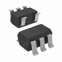
5-Pin SOT-23 (DBV) Package
2 Applications
•
•
•
•
ADAS Modules
RF Modules
Wireless Modules
General Noise-Sensitive Applications
A combination of new circuit design and process
innovation has enabled the usual PNP pass transistor
to be replaced by a PMOS pass element. Because
the PMOS pass element behaves as a low-value
resistor, the dropout voltage is very low, typically
71 mV at 100 mA of load current (TPS76950-Q1),
and is directly proportional to the load current.
Because the PMOS pass element is a voltage-driven
device, the quiescent current is ultralow (28 µA
maximum) and is stable over the entire range of
output load current (0 mA to 100 mA). The ultralowdropout voltage feature and ultralow-power operation
result in a significant increase in system battery
operating life, making this device suitable for use in
automotive applications.
Device Information(1)
PART NUMBER
TPS769xx-Q1
PACKAGE
BODY SIZE (NOM)
SOT-23 (5)
2.90 mm × 1.60 mm
(1) For all available packages, see the orderable addendum at
the end of the data sheet.
Functional Block Diagrams
TPS76933-Q1 Ground Current vs Free-Air
Temperature
TPS76901-Q1
22
OUT
IN
EN
21
Current Limit
/ Thermal
Protection
VREF
V I = 4.3 V
C O = 4.7 µF
20
FB
Ground Current − µA
GND
TPS769xx-Q1
OUT
IN
19
I O = 100 mA
18
I O = 0 mA
17
EN
VREF
Current Limit
/ Thermal
Protection
16
15
GND
−60 −40 −20
0
20
40
60
80
100
120 140
TA − Free-Air Temperature − °C
Copyright © 2016, Texas Instruments Incorporated
1
An IMPORTANT NOTICE at the end of this data sheet addresses availability, warranty, changes, use in safety-critical applications,
intellectual property matters and other important disclaimers. PRODUCTION DATA.
�TPS76901-Q1, TPS76912-Q1, TPS76915-Q1
TPS76918-Q1, TPS76925-Q1, TPS76927-Q1
TPS76928-Q1, TPS76930-Q1, TPS76933-Q1, TPS76950-Q1
SGLS118D – DECEMBER 2001 – REVISED SEPTEMBER 2016
www.ti.com
Table of Contents
1
2
3
4
5
6
7
8
Features ..................................................................
Applications ...........................................................
Description .............................................................
Revision History.....................................................
Description (continued).........................................
Pin Configuration and Functions .........................
Specifications.........................................................
1
1
1
2
3
3
3
7.1
7.2
7.3
7.4
7.5
7.6
7.7
3
3
4
4
4
6
6
Absolute Maximum Ratings ......................................
ESD Ratings..............................................................
Recommended Operating Conditions.......................
Thermal Information ..................................................
Electrical Characteristics...........................................
Dissipation Ratings ...................................................
Typical Characteristics ..............................................
Detailed Description ............................................ 10
8.1 Overview ................................................................. 10
8.2 Functional Block Diagrams ..................................... 10
8.3 Feature Description................................................. 10
8.4 Device Functional Modes........................................ 10
9
Application and Implementation ........................ 11
9.1 Application Information............................................ 11
9.2 Typical Application .................................................. 11
10 Power Supply Recommendations ..................... 13
11 Layout................................................................... 14
11.1 Layout Guidelines ................................................. 14
11.2 Layout Example .................................................... 14
11.3 Power Dissipation and Junction Temperature ...... 14
12 Device and Documentation Support ................. 15
12.1
12.2
12.3
12.4
12.5
12.6
Related Links ........................................................
Receiving Notification of Documentation Updates
Community Resources..........................................
Trademarks ...........................................................
Electrostatic Discharge Caution ............................
Glossary ................................................................
15
15
15
15
15
15
13 Mechanical, Packaging, and Orderable
Information ........................................................... 15
4 Revision History
NOTE: Page numbers for previous revisions may differ from page numbers in the current version.
Changes from Revision C (June 2012) to Revision D
Page
•
Added ESD Ratings table, Thermal Information table, Feature Description section, Device Functional Modes,
Application and Implementation section, Power Supply Recommendations section, Layout section, Device and
Documentation Support section, and Mechanical, Packaging, and Orderable Information section....................................... 1
•
Removed Ordering Information table, see POA at the end of the data sheet........................................................................ 1
Changes from Revision B (April 2008) to Revision C
Page
•
Changed TPS769xx part names to TPS769xx-Q1 in text and images. ................................................................................. 3
•
Updated Figures 17 and 19 to include region of Instability below 0.2 Ω................................................................................ 9
2
Submit Documentation Feedback
Copyright © 2001–2016, Texas Instruments Incorporated
Product Folder Links: TPS76901-Q1 TPS76912-Q1 TPS76915-Q1 TPS76918-Q1 TPS76925-Q1 TPS76927-Q1
TPS76928-Q1 TPS76930-Q1 TPS76933-Q1 TPS76950-Q1
�TPS76901-Q1, TPS76912-Q1, TPS76915-Q1
TPS76918-Q1, TPS76925-Q1, TPS76927-Q1
TPS76928-Q1, TPS76930-Q1, TPS76933-Q1, TPS76950-Q1
www.ti.com
SGLS118D – DECEMBER 2001 – REVISED SEPTEMBER 2016
5 Description (continued)
The TPS769xx-Q1 devices also feature a logic-enabled sleep mode to shut down the regulator, reducing
quiescent current to 1 µA (typical) at TJ = 25°C. The TPS769xx-Q1 devices are offered in 1.2-V, 1.5-V, 1.8-V,
2.5‑V, 2.7-V, 2.8-V, 3-V, 3.3-V, and 5-V fixed-voltage versions and in a variable version (programmable over the
range of 1.2 V to 5.5 V).
6 Pin Configuration and Functions
DBV Package
5-Pin SOT-23
Top View
IN
1
GND
2
EN
3
5
OUT
4
FB/NC
Not to scale
Pin Functions
PIN
NO.
NAME
I/O
DESCRIPTION
1
IN
I
2
GND
—
Input supply voltage
3
EN
I
Enable input
4
FB/NC
I
Feedback voltage (TPS76901-Q1 only)
No connection (Fixed options only)
5
OUT
O
Regulated output voltage
Ground
7 Specifications
7.1 Absolute Maximum Ratings
over operating free-air temperature range (unless otherwise noted) (1)
MIN
MAX
UNIT
Input voltage (2)
–0.3
13.5
V
Voltage range at EN
–0.3
VI + 0.3
V
7
V
Voltage on OUT, FB
Peak output current
Internally Limited
Continuous total power dissipation
See Dissipation Ratings
TJ
Operating virtual junction temperature
–40
150
°C
Tstg
Storage temperature
–65
150
°C
(1)
(2)
Stresses beyond those listed under Absolute Maximum Ratings may cause permanent damage to the device. These are stress ratings
only, and functional operation of the device at these or any other conditions beyond those indicated under Recommended Operating
Conditions is not implied. Exposure to absolute-maximum-rated conditions for extended periods may affect device reliability.
All voltage values are with respect to network ground terminal.
7.2 ESD Ratings
VALUE
V(ESD)
(1)
(2)
Electrostatic discharge
Human-body model (HBM), per ANSI/ESDA/JEDEC JS-001 (1)
±2000
Charged-device model (CDM), per JEDEC specification JESD22-C101 (2)
±YYY
UNIT
V
JEDEC document JEP155 states that 500-V HBM allows safe manufacturing with a standard ESD control process.
JEDEC document JEP157 states that 250-V CDM allows safe manufacturing with a standard ESD control process.
Copyright © 2001–2016, Texas Instruments Incorporated
Submit Documentation Feedback
Product Folder Links: TPS76901-Q1 TPS76912-Q1 TPS76915-Q1 TPS76918-Q1 TPS76925-Q1 TPS76927-Q1
TPS76928-Q1 TPS76930-Q1 TPS76933-Q1 TPS76950-Q1
3
�TPS76901-Q1, TPS76912-Q1, TPS76915-Q1
TPS76918-Q1, TPS76925-Q1, TPS76927-Q1
TPS76928-Q1, TPS76930-Q1, TPS76933-Q1, TPS76950-Q1
SGLS118D – DECEMBER 2001 – REVISED SEPTEMBER 2016
www.ti.com
7.3 Recommended Operating Conditions
over operating free-air temperature range (unless otherwise noted)
MIN
(1)
VI
Input voltage
VO
Output voltage
IO
Continuous output current (2)
TJ
Operating junction temperature
(1)
(2)
MAX
UNIT
2.7
10
1.2
5.5
V
V
0
100
mA
—40
125
°C
To calculate the minimum input voltage for your maximum output current, use the following formula: VI(min) = VO(max) + VDO(max load)
Continuous output current and operating junction temperature are limited by internal protection circuitry, but it is not recommended that
the device operate under conditions beyond those specified in this table for extended periods of time.
7.4 Thermal Information
TPS769xx-Q1
THERMAL METRIC (1)
DBV (SOT-23)
UNIT
5 PINS
RθJA
Junction-to-ambient thermal resistance
204.6
°C/W
RθJC(top)
Junction-to-case (top) thermal resistance
117.5
°C/W
RθJB
Junction-to-board thermal resistance
34.4
°C/W
ψJT
Junction-to-top characterization parameter
11.8
°C/W
ψJB
Junction-to-board characterization parameter
33.5
°C/W
RθJC(bot)
Junction-to-case (bottom) thermal resistance
—
°C/W
(1)
For more information about traditional and new thermal metrics, see the Semiconductor and IC Package Thermal Metrics application
report.
7.5 Electrical Characteristics
over recommended operating free-air temperature range, VI = VO (typ) + 1 V, IO = 100 mA, EN = 0 V, Co = 4.7 µF (unless
otherwise noted)
PARAMETER
TPS76901-Q1
TPS76912-Q1
TPS76915-Q1
TPS76918-Q1
Output voltage
(10 ∝A to 100 mA
load) (1)
TPS76925-Q1
TPS76927-Q1
TPS76928-Q1
TPS76930-Q1
TPS76933-Q1
TPS76950-Q1
(1)
4
TEST CONDITIONS
MIN
1.2 V ≤ VO ≤ 5.5 V, TJ = 25°C
1.2 V ≤ VO ≤ 5.5 V, TJ = –40°C to 125°C
1.455
1.746
2.425
2.619
2.781
2.716
2.884
3
2.91
3.09
3.3
3.201
TJ = 25°C, 6 V < VIN < 10 V
TJ = —40°C to 125°C, 6 V < VIN < 10 V
V
2.8
TJ = 25°C, 4.3 V < VIN < 10 V
TJ = –40°C to 125°C, 4.3 V < VIN < 10 V
2.575
2.7
TJ = 25°C, 4 V < VIN < 10 V
TJ = –40°C to 125°C, 4 V < VIN < 10 V
1.854
2.5
TJ = 25°C, 3.8 V < VIN < 10 V
TJ = –40°C to 125°C, 3.8 V < VIN < 10 V
1.545
1.8
TJ = 25°C, 3.7 V < VIN < 10 V
TJ = –40°C to 125°C, 3.7 V < VIN < 10 V
1.261
1.5
TJ = 25°C, 3.5 V < VIN < 10 V
TJ = –40°C to 125°C, 3.5 V < VIN < 10 V
1.03 VO
1.187
TJ = 25°C, 2.8 V < VIN < 10 V
TJ = –40°C to 125°C, 2.8 V < VIN < 10 V
UNIT
1.224
TJ = 25°C, 2.7 V < VIN < 10 V
TJ = –40°C to 125°C, 2.7 V < VIN < 10 V
MAX
VO
0.97 VO
TJ = 25°C, 2.7 V < VIN < 10 V
TJ = –40°C to 125°C, 2.7 V < VIN < 10 V
TYP
3.399
5
4.85
5.15
Minimum IN operating voltage is 2.7 V or VO (typ) + 1 V, whichever is greater. The maximum IN voltage is 10 V, minimum output current
is 10 µA, and maximum output current is 100 mA.
Submit Documentation Feedback
Copyright © 2001–2016, Texas Instruments Incorporated
Product Folder Links: TPS76901-Q1 TPS76912-Q1 TPS76915-Q1 TPS76918-Q1 TPS76925-Q1 TPS76927-Q1
TPS76928-Q1 TPS76930-Q1 TPS76933-Q1 TPS76950-Q1
�TPS76901-Q1, TPS76912-Q1, TPS76915-Q1
TPS76918-Q1, TPS76925-Q1, TPS76927-Q1
TPS76928-Q1, TPS76930-Q1, TPS76933-Q1, TPS76950-Q1
www.ti.com
SGLS118D – DECEMBER 2001 – REVISED SEPTEMBER 2016
Electrical Characteristics (continued)
over recommended operating free-air temperature range, VI = VO (typ) + 1 V, IO = 100 mA, EN = 0 V, Co = 4.7 µF (unless
otherwise noted)
PARAMETER
TEST CONDITIONS
MIN
TYP
Quiescent current
(GND current) (1) (2)
EN = 0 V, 0 mA < IO < 100 mA, TJ = 25°C
Load regulation
EN = 0 V, IO = 0 to 100 mA, TJ = 25°C
Output voltage line regulation
(∆VO/VO) (2)
VO + 1 V < VI ≤ 10 V, TJ = 25°C (1)
Output noise voltage
BW = 300 Hz to 50 kHz, Co = 10 ∝F, TJ = 25°C
190
Output current limit
VO = 0 V (1)
350
EN = 0 V, IO = 100 mA, TJ = –40°C to 125°C
12
VO + 1 V < VI ≤ 10 V, TJ = –40°C to 125°C (1)
–1
2.7 V < VI < 10 V
1.7
Low level enable input voltage
2.7 V < VI < 10 V
Power supply ripple rejection
f = 1 kHz, Co = 10 ∝F, TJ = 25°C
1
0.9
–1
EN = VI
–1
0
TPS76933-Q1
245
115
115
230
48
TPS76950-Q1
100
IO = 100 mA, TJ = –40°C to 125°C
(2)
200
35
IO = 50 mA, TJ = –40°C to 125°C
IO = 100 mA, TJ = 25°C
mV
98
IO = 100 mA, TJ = –40°C to 125°C
IO = 50 mA, TJ = 25°C
µA
57
IO = 50 mA, TJ = –40°C to 125°C
IO = 100 mA, TJ = 25°C
1
125
IO = 50 mA, TJ = –40°C to 125°C
IO = 50 mA, TJ = 25°C
V
122
IO = 100 mA, TJ = –40°C to 125°C
Dropout voltage (3)
µA
60
IO = 50 mA, TJ = –40°C to 125°C
IO = 100 mA, TJ = 25°C
µA
dB
1
IO = 100 mA, TJ = –40°C to 125°C
TPS76930-Q1
mA
V
60
EN = 0 V
IO = 50 mA, TJ = 25°C
µVrms
750
2
FB = 1.224 V (TPS76901-Q1)
IO = 100 mA, TJ = 25°C
%/V
1
High level enable input voltage
TPS76928-Q1
mV
0.1
FB input current
IO = 50 mA, TJ = 25°C
µA
0.04
TJ = —40°C to 125°C
Input current (EN)
UNIT
28
EN = VI, 2.7 < VI < 10 V
Standby current
MAX
17
85
71
170
If VO ≤ 1.8 V then VImin = 2.7 V, VImax = 10 V:
Line Reg. (mV) = (% / V) ´
VO (Vlmax - 2.7 V)
´ 1000
100
If VO ≥ 2.5 V then VImin = VO + 1 V, VImax = 10 V:
Line Reg. (mV) = (% / V) ´
(3)
VO (Vlmax - (VO + 1V))
´ 1000
100
The IN voltage equals VO (typ) — 100 mV; the TPS76901-Q1 output voltage is set to 3.3 V nominal with an external resistor divider.
TPS76912-Q1, TPS76915-Q1, TPS76918-Q1, TPS76925-Q1, and TPS76927-Q1 dropout voltage is limited by input voltage range
limitations.
Copyright © 2001–2016, Texas Instruments Incorporated
Submit Documentation Feedback
Product Folder Links: TPS76901-Q1 TPS76912-Q1 TPS76915-Q1 TPS76918-Q1 TPS76925-Q1 TPS76927-Q1
TPS76928-Q1 TPS76930-Q1 TPS76933-Q1 TPS76950-Q1
5
�TPS76901-Q1, TPS76912-Q1, TPS76915-Q1
TPS76918-Q1, TPS76925-Q1, TPS76927-Q1
TPS76928-Q1, TPS76930-Q1, TPS76933-Q1, TPS76950-Q1
SGLS118D – DECEMBER 2001 – REVISED SEPTEMBER 2016
www.ti.com
7.6 Dissipation Ratings
BOARD
PACKAGE
RθJC
RθJA
DERATING FACTOR
ABOVE TA = 25°C
TA ≤ 25°C
POWER
RATING
TA = 70°C
POWER
RATING
TA = 85°C
POWER
RATING
Low K (1)
DBV
65.8°C/W
259°C/W
3.9 mW/°C
386 mW
212 mW
154 mW
(2)
DBV
65.8°C/W
180°C/W
5.6 mW/°C
555 mW
305 mW
222 mW
High K
(1)
(2)
The JEDEC Low K (1s) board design used to derive this data was a 3 inch x 3 inch, two layer board with 2 ounce copper traces on top
of the board.
The JEDEC High K (2s2p) board design used to derive this data was a 3 inch x 3 inch, multilayer board with 1 ounce internal power and
ground planes and 2 ounce copper traces on top and bottom of the board.
7.7 Typical Characteristics
2.498
1.498
V I = 3.5 V
C O = 4.7 µF
TA = 25 °C
2.496
V I = 2.7 V
C O = 4.7 µF
TA = 25 °C
1.496
2.494
VO − Output Voltage − V
V O − Output Voltage − V
1.494
2.492
2.490
2.488
2.486
1.492
1.490
1.488
1.486
2.484
1.484
2.482
0
20
40
60
80
0
100
20
40
60
Figure 1. TPS76925-Q1 Output Voltage vs Output Current
1.496
V I = 4.3 V
C O = 4.7 µF
TA = 25 °C
3.282
1.494
I O = 1 mA
V I = 2.7 V
C O = 4.7 µF
1.492
VO − Output Voltage − V
3.280
V O − Output Voltage − V
100
Figure 2. TPS76915-Q1 Output Voltage vs Output Current
3.284
3.278
3.276
3.274
3.272
1.490
1.488
1.486
I O = 100 mA
1.484
1.482
3.270
0
20
40
60
80
100
I O − Output Current − mA
Figure 3. TPS76933-Q1 Output Voltage vs Output Current
6
80
I O − Output Current − mA
I O − Output Current − mA
Submit Documentation Feedback
1.480
−60
−40
−20
0
20
40
60
80
100
120
140
TA − Free-Air Temperature −°C
Figure 4. TPS76915-Q1 Output Voltage vs Free-Air
Temperature
Copyright © 2001–2016, Texas Instruments Incorporated
Product Folder Links: TPS76901-Q1 TPS76912-Q1 TPS76915-Q1 TPS76918-Q1 TPS76925-Q1 TPS76927-Q1
TPS76928-Q1 TPS76930-Q1 TPS76933-Q1 TPS76950-Q1
�TPS76901-Q1, TPS76912-Q1, TPS76915-Q1
TPS76918-Q1, TPS76925-Q1, TPS76927-Q1
TPS76928-Q1, TPS76930-Q1, TPS76933-Q1, TPS76950-Q1
www.ti.com
SGLS118D – DECEMBER 2001 – REVISED SEPTEMBER 2016
Typical Characteristics (continued)
2.496
3.285
2.494
I O = 1 mA
IO = 1 mA
3.280
2.492
VO − Output Voltage − V
VO − Output Voltage − V
2.490
2.488
2.486
2.484
IO = 100 mA
2.482
2.480
2.476
−60
3.270
IO = 100 mA
3.265
3.260
V I = 3.5 V
C O = 4.7 µF
2.478
V I = 4.3 V
C O = 4.7 µF
3.275
3.255
−40 −20
0
20
40
60
80
100
120
−60 −40 −20
140
0
20
40
60
80
100
120
140
TA − Free-Air Temperature − °C
TA − Free-Air Temperature − °C
Figure 5. TPS76925-Q1 Output Voltage vs Free-Air
Temperature
Figure 6. TPS76933-Q1 Output Voltage vs Free-Air
Temperature
22
2
V I = 4.3 V
C O = 4.7 µF
1.8
Output Spectral Noise Density − µV Hz
21
Ground Current − µA
20
I O = 100 mA
19
18
I O = 0 mA
17
16
15
−60
−40
0
−20
20
40
60
80
100
120
C O = 4.7 µF
I O = 100 mA
1.4
1.2
1
0.8
C O = 4.7 µF
I O = 1 mA
0.6
0.4
0.2
C O = 10 µF
I O = 100 mA
V I = 4.3 V
0
100
140
1k
10k
100k
f − Frequency − Hz
TA − Free-Air Temperature − °C
Figure 7. TPS76933-Q1 Ground Current vs Free-Air
Temperature
Figure 8. TPS76933-Q1 Output Spectral Noise Density vs
Frequency
2
1000
V I = 3.2 V
C O = 4.7 µF
1.6
VDO − Dropout Voltage − mV
V I = 4.3 V
C O = 4.7 µF
ESR = 0.3 Ω
TA = 25 °C
1.8
Z o − Output Impedance − Ω
C O = 10 µF
I O = 1 mA
1.6
1.4
1.2
1
0.8
I O = 1 mA
0.6
100
I O = 100 mA
10
I O = 10 mA
0.4
I O = 100 mA
0.2
0
10
100
1k
10 k
100 k
1M
1
−60 −40
−20
0
20
40
60
80
100
120
140
f − Frequency − Hz
TA − Free-Air Temperature − °C
Figure 9. Output Impedance vs Frequency
Figure 10. TPS76933-Q1 Dropout Voltage vs Free-Air
Temperature
Copyright © 2001–2016, Texas Instruments Incorporated
Submit Documentation Feedback
Product Folder Links: TPS76901-Q1 TPS76912-Q1 TPS76915-Q1 TPS76918-Q1 TPS76925-Q1 TPS76927-Q1
TPS76928-Q1 TPS76930-Q1 TPS76933-Q1 TPS76950-Q1
7
�TPS76901-Q1, TPS76912-Q1, TPS76915-Q1
TPS76918-Q1, TPS76925-Q1, TPS76927-Q1
TPS76928-Q1, TPS76930-Q1, TPS76933-Q1, TPS76950-Q1
SGLS118D – DECEMBER 2001 – REVISED SEPTEMBER 2016
www.ti.com
Typical Characteristics (continued)
100
90
80
EN
Ripple Rejection − dB
70
I O = 1 mA
60
50
40
30
I O = 100 mA
20
10
V I = 4.3 V
C O = 4.7 µF
ESR = 0.3 Ω
0
VO
−10
10
100
1k
10 k
100 k
1M
10 M
0
20
40
60
f − Frequency − Hz
10
0
−10
∆ V O − Change In
Output Voltage − mV
V I − Input Voltage − V
3.7
2.7
I L = 10 mA
C O = 4.7 µF
ESR = 0.3 Ω
20
40
60
80
100
120
140
160
180
−10
4.3
I L = 10 mA
C O = 4.7 µF
ESR = 0.3 Ω
100
120
140
160
180
t − Time − µs
Figure 15. TPS76933-Q1 Line Transient Response
8
200
−200
V I = 2.7 V
C O = 10 µF
ESR = 0.3 Ω
−400
0
20
40
60
80
100
120
140
160
180
200
Figure 14. TPS76915-Q1 Load Transient Response
∆ V O − Change In
Output Voltage − mV
V I − Input Voltage − V
5.3
80
180
0
Current Load − mA
V O − Output Voltage − mV
0
60
160
t − Time − µs
10
40
140
0
200
Figure 13. TPS76915-Q1 Line Transient Response
20
120
100
t − Time − µs
0
100
Figure 12. LDO Start-Up Time
Current Load − mA
V O − Output Voltage − mV
Figure 11. TPS76933-Q1 Ripple Rejection vs Frequency
0
80
t − Time − µs
Submit Documentation Feedback
100
0
V I = 4.3 V
C O = 4.7 µF
ESR = 0.3 Ω
100
0
−100
0
20
40
60
80
100
120
140
160
180
t − Time − µs
Figure 16. TPS76933-Q1 Load Transient Response
Copyright © 2001–2016, Texas Instruments Incorporated
Product Folder Links: TPS76901-Q1 TPS76912-Q1 TPS76915-Q1 TPS76918-Q1 TPS76925-Q1 TPS76927-Q1
TPS76928-Q1 TPS76930-Q1 TPS76933-Q1 TPS76950-Q1
�TPS76901-Q1, TPS76912-Q1, TPS76915-Q1
TPS76918-Q1, TPS76925-Q1, TPS76927-Q1
TPS76928-Q1, TPS76930-Q1, TPS76933-Q1, TPS76950-Q1
www.ti.com
SGLS118D – DECEMBER 2001 – REVISED SEPTEMBER 2016
Typical Characteristics (continued)
100
V IN = 4.3 V
C O = 4.7 µF
3.3 V LDO
ESR − Equivalent Series Resistance − Ω
ESR − Equivalent Series Resistance − Ω
100
Region of Instability
10
Region of Stability
1
V IN = 4.3 V
C O = 4.7 µF
I L = 100 mA
Region of Instability
10
Region of Stability
0.2
0.1
0
25
75
50
1
100
0
0.1
I O − Output Current − mA
Figure 17. TPS76933-Q1 Typical Regions of Stability
Equivalent Series Resistance (ESR) vs Output Current
0.3
0.4
0.5
0.6
0.7
0.8
0.9
1
Figure 18. TPS76933-Q1 Typical Regions of Stability
Equivalent Series Resistance (ESR) vs Added Ceramic
Capacitance
100
100
V IN = 4.3 V
C O = 10 µF
3.3 V LDO
ESR − Equivalent Series Resistance − Ω
ESR − Equivalent Series Resistance − Ω
0.2
Added Ceramic Capacitance − µF
Region of Instability
10
1
Region of Stability
V IN = 4.3 V
C O = 10 µF
I L = 100 mA
Region of Instability
10
Region of Stability
0.2
0.1
1
0
25
50
75
100
I O − Output Current − mA
Figure 19. TPS76933-Q1 Typical Regions of Stability
Equivalent Series Resistance (ESR) vs Output Current
Copyright © 2001–2016, Texas Instruments Incorporated
0
0.1
0.2
0.3
0.4
0.5
0.6
0.7
0.8
0.9
1
Added Ceramic Capacitance − µF
Figure 20. TPS76933-Q1 Typical Regions of Stability
Equivalent Series Resistance (ESR) vs Added Ceramic
Capacitance
Submit Documentation Feedback
Product Folder Links: TPS76901-Q1 TPS76912-Q1 TPS76915-Q1 TPS76918-Q1 TPS76925-Q1 TPS76927-Q1
TPS76928-Q1 TPS76930-Q1 TPS76933-Q1 TPS76950-Q1
9
�TPS76901-Q1, TPS76912-Q1, TPS76915-Q1
TPS76918-Q1, TPS76925-Q1, TPS76927-Q1
TPS76928-Q1, TPS76930-Q1, TPS76933-Q1, TPS76950-Q1
SGLS118D – DECEMBER 2001 – REVISED SEPTEMBER 2016
www.ti.com
8 Detailed Description
8.1 Overview
The TPS769xx-Q1 family of low-dropout (LDO) regulators are optimized for use in battery-operated equipment
and automotive applications. They feature extremely low dropout voltages, low quiescent current (17 µA
nominally), and enable inputs to reduce supply currents to 1 µA when the regulators are turned off.
8.2 Functional Block Diagrams
OUT
IN
EN
VREF
Current Limit
/ Thermal
Protection
FB
GND
Copyright © 2016, Texas Instruments Incorporated
Figure 21. TPS76901-Q1 Functional Block Diagram
OUT
IN
EN
VREF
Current Limit
/ Thermal
Protection
GND
Copyright © 2016, Texas Instruments Incorporated
Figure 22. TPS769xx-Q1 Functional Block Diagram
8.3 Feature Description
8.3.1 Regulator Protection
The TPS769xx-Q1 PMOS-pass transistor has a built-in back diode that conducts reverse current when the input
voltage drops below the output voltage (for example, during power down). Current is conducted from the output
to the input and is not internally limited. If extended reverse voltage operation is anticipated, external limiting
might be appropriate.
The TPS769xx-Q1 features internal current limiting and thermal protection. During normal operation, the
TPS769xx-Q1 limits output current to approximately 350 mA. When current limiting engages, the output voltage
scales back linearly until the overcurrent condition ends. While current limiting is designed to prevent gross
device failure, care must be taken not to exceed the power dissipation ratings of the package. If the temperature
of the device exceeds approximately 165°C, thermal-protection circuitry shuts it down. Once the device has
cooled down to below approximately 140°C, regulator operation resumes.
8.4 Device Functional Modes
At 100-mA loads the device operates in low power mode and the quiescent current consumption is reduced to
28 µA (maximum).
10
Submit Documentation Feedback
Copyright © 2001–2016, Texas Instruments Incorporated
Product Folder Links: TPS76901-Q1 TPS76912-Q1 TPS76915-Q1 TPS76918-Q1 TPS76925-Q1 TPS76927-Q1
TPS76928-Q1 TPS76930-Q1 TPS76933-Q1 TPS76950-Q1
�TPS76901-Q1, TPS76912-Q1, TPS76915-Q1
TPS76918-Q1, TPS76925-Q1, TPS76927-Q1
TPS76928-Q1, TPS76930-Q1, TPS76933-Q1, TPS76950-Q1
www.ti.com
SGLS118D – DECEMBER 2001 – REVISED SEPTEMBER 2016
9 Application and Implementation
NOTE
Information in the following applications sections is not part of the TI component
specification, and TI does not warrant its accuracy or completeness. TI’s customers are
responsible for determining suitability of components for their purposes. Customers should
validate and test their design implementation to confirm system functionality.
9.1 Application Information
The TPS769xx-Q1 uses a PMOS pass element to dramatically reduce both dropout voltage and supply current
over more conventional PNP-pass-element LDO designs. The PMOS pass element is a voltage-controlled device
and, unlike a PNP transistor, it does not require increased drive current as output current increases. Supply
current in the TPS769xx-Q1 is essentially constant from no load to maximum load.
Current limiting and thermal protection prevent damage by excessive output current and/or power dissipation.
The device switches into a constant-current mode at approximately 350 mA; further load reduces the output
voltage instead of increasing the output current. The thermal protection shuts the regulator off if the junction
temperature rises above approximately 165°C. Recovery is automatic when the junction temperature drops
approximately 25°C below the high temperature trip point. The PMOS pass element includes a back gate diode
that conducts reverse current when the input voltage level drops below the output voltage level.
A voltage of 1.7 V or greater on the EN input disables the TPS769xx-Q1 internal circuitry, reducing the supply
current to 1 µA. A voltage of less than 0.9 V on the EN input enables the TPS769xx and enables normal
operation to resume. The EN input does not include any deliberate hysteresis, and it exhibits an actual switching
threshold of approximately 1.5 V.
9.2 Typical Application
TPS769xx-Q1
1
VI
IN
NC/FB
OUT
C1
1 µF
4
5
VO
3
EN
+
4.7 µF
GND
2
ESR = 0.2 Ω
Copyright © 2016, Texas Instruments Incorporated
TPS76912-Q1, TPS76915-Q1, TPS76918-Q1, TPS76925-Q1, TPS76927-Q1, TPS76928-Q1, TPS76930-Q1,
TPS76933-Q1, TPS76950-Q1 (fixed-voltage options).
Figure 23. Typical Application Circuit
Copyright © 2001–2016, Texas Instruments Incorporated
Submit Documentation Feedback
Product Folder Links: TPS76901-Q1 TPS76912-Q1 TPS76915-Q1 TPS76918-Q1 TPS76925-Q1 TPS76927-Q1
TPS76928-Q1 TPS76930-Q1 TPS76933-Q1 TPS76950-Q1
11
�TPS76901-Q1, TPS76912-Q1, TPS76915-Q1
TPS76918-Q1, TPS76925-Q1, TPS76927-Q1
TPS76928-Q1, TPS76930-Q1, TPS76933-Q1, TPS76950-Q1
SGLS118D – DECEMBER 2001 – REVISED SEPTEMBER 2016
www.ti.com
Typical Application (continued)
9.2.1 Design Requirements
Table 1 lists the design parameters for this example.
Table 1. Design Parameters
PARAMETER
EXAMPLE VALUE
Input voltage range
4 V to 10 V
Output voltage
2.5 V to 5 V
Output current rating
100 mA
Output capacitor
4.7 µF to 10 µF
Output capacitor ESD range
200 mΩ to 10 Ω
9.2.2 Detailed Design Procedure
9.2.2.1 External Capacitor Requirements
Although not required, TI recommends a 0.047-µF or larger ceramic input bypass capacitor, connected between
IN and GND and located close to the TPS769xx-Q1, to improve transient response and noise rejection. A highervalue electrolytic input capacitor may be necessary if large, fast-rise-time load transients are anticipated and the
device is located several inches from the power source.
Like all low dropout regulators, the TPS769xx-Q1 requires an output capacitor connected between OUT and
GND to stabilize the internal control loop. The minimum recommended capacitance is 4.7 µF. The ESR
(equivalent series resistance) of the capacitor must be between 0.2 Ω and 10 Ω. to ensure stability. Capacitor
values larger than 4.7 µF are acceptable, and allow the use of smaller ESR values. Capacitances less than
4.7 µF are not recommended because they require careful selection of ESR to ensure stability. Solid tantalum
electrolytic, aluminum electrolytic, and multilayer ceramic capacitors are all suitable, provided they meet the
requirements described above. Most of the commercially available 4.7-µF surface-mount solid tantalum
capacitors, including devices from Sprague, Kemet, and Nichico, meet the ESR requirements stated above.
Multilayer ceramic capacitors may have very small equivalent series resistances and may therefore require the
addition of a low value series resistor to ensure stability.
Table 2. Capacitor Selection
MFR.
VALUE
MAX ESR
SIZE (H × L × W) (1)
T494B475K016AS
KEMET
4.7 µF
1.5 Ω
1.9 × 3.5 × 2.8
195D106x0016x2T
SPRAGUE
10 µF
1.5 Ω
1.3 × 7 × 2.7
695D106x003562T
SPRAGUE
10 µF
1.3 Ω
2.5 × 7.6 × 2.5
AVX
4.7 µF
0.6 Ω
2.6 × 6 × 3.2
PART NO.
TPSC475K035R0600
(1)
Size is in mm. ESR is maximum resistance in Ω at 100 kHz and TA = 25°C. Contact manufacturer for minimum ESR values.
9.2.2.2 Output Voltage Programming
The output voltage of the TPS76901-Q1 adjustable regulator is programmed using an external resistor divider as
shown in Figure 24. The output voltage is calculated using Equation 1.
R1
VO = Vref ´ (1 +
)
R2
where
•
The internal reference voltage (VREF) = 1.224 V (typical)
(1)
Resistors R1 and R2 must be chosen for approximately 7-µA divider current. Lower value resistors can be used
but offer no inherent advantage and waste more power. Higher values must be avoided as leakage currents at
FB increase the output voltage error. The recommended design procedure is to choose R2 = 169 kΩ to set the
divider current at 7 µA and then calculate R1 using Equation 2.
V
R1 = ( O - 1) ´ R2
Vref
(2)
12
Submit Documentation Feedback
Copyright © 2001–2016, Texas Instruments Incorporated
Product Folder Links: TPS76901-Q1 TPS76912-Q1 TPS76915-Q1 TPS76918-Q1 TPS76925-Q1 TPS76927-Q1
TPS76928-Q1 TPS76930-Q1 TPS76933-Q1 TPS76950-Q1
�TPS76901-Q1, TPS76912-Q1, TPS76915-Q1
TPS76918-Q1, TPS76925-Q1, TPS76927-Q1
TPS76928-Q1, TPS76930-Q1, TPS76933-Q1, TPS76950-Q1
www.ti.com
SGLS118D – DECEMBER 2001 – REVISED SEPTEMBER 2016
Table 3. Output Voltage Programming Guide
DIVIDER RESISTANCE (kΩ) (1)
OUTPUT VOLTAGE (V)
(1)
R1
R2
2.5
174
169
3.3
287
169
3.6
324
169
4
383
169
5
523
169
1% values shown.
TPS76901-Q1
VI
1 µF
1
IN
OUT
≥ 1.7 V
3
5
VO
R1
EN
FB
≤ 0.9 V
GND
2
4
4.7 µF
R2
ESR = 0.2 Ω
Copyright © 2016, Texas Instruments Incorporated
Figure 24. TPS76901-Q1 Adjustable LDO Regulator Programming
9.2.3 Application Curves
Figure 25. Power-Up Waveform
(CH1 VOUT, CH2 VIN, CH4 IOUT)
Figure 26. Power-Down Waveform
(CH1 VOUT, CH2 VIN, CH4 IOUT)
10 Power Supply Recommendations
Design of the device is for operation from an input voltage supply with a range between 2.7 V and 10 V. This
input supply must be well regulated. If the input supply is located more than a few inches from the device, TI
recommends adding an electrolytic capacitor with a value of 1 µF and a ceramic bypass capacitor at the input.
Copyright © 2001–2016, Texas Instruments Incorporated
Submit Documentation Feedback
Product Folder Links: TPS76901-Q1 TPS76912-Q1 TPS76915-Q1 TPS76918-Q1 TPS76925-Q1 TPS76927-Q1
TPS76928-Q1 TPS76930-Q1 TPS76933-Q1 TPS76950-Q1
13
�TPS76901-Q1, TPS76912-Q1, TPS76915-Q1
TPS76918-Q1, TPS76925-Q1, TPS76927-Q1
TPS76928-Q1, TPS76930-Q1, TPS76933-Q1, TPS76950-Q1
SGLS118D – DECEMBER 2001 – REVISED SEPTEMBER 2016
www.ti.com
11 Layout
11.1 Layout Guidelines
For the LDO power supply, especially these high voltage and large current ones, layout is an important step. If
layout is not carefully designed, the regulator could not deliver enough output current because of the thermal
limitation. To improve the thermal performance of the device, and maximize the current output at high ambient
temperature, it is recommended to spread the GND as large as possible and put enough thermal vias on the
thermal pad. Figure 27 shows an example layout.
11.2 Layout Example
IN
OUT
GND
NC/FB
EN
Figure 27. Layout Recommendation
11.3 Power Dissipation and Junction Temperature
Specified regulator operation is assured to a junction temperature of 125°C; the maximum junction temperature
must be restricted to 125°C under normal operating conditions. This restriction limits the power dissipation the
regulator can handle in any given application. To ensure the junction temperature is within acceptable limits,
calculate the maximum allowable dissipation, PD(max), and the actual dissipation, PD, which must be less than or
equal to PD(max).
The maximum-power-dissipation limit is determined using Equation 3.
T max - TA
PD(max) = J
RqJA
where
•
•
•
TJmax is the maximum allowable junction temperature
RθJA is the thermal resistance junction-to-ambient for the package, see the dissipation rating table.
TA is the ambient temperature.
The regulator dissipation is calculated using Equation 4.
PD = (VI - VO ) ´ IO
(3)
(4)
Power dissipation resulting from quiescent current is negligible. Excessive power dissipation triggers the thermal
protection circuit.
14
Submit Documentation Feedback
Copyright © 2001–2016, Texas Instruments Incorporated
Product Folder Links: TPS76901-Q1 TPS76912-Q1 TPS76915-Q1 TPS76918-Q1 TPS76925-Q1 TPS76927-Q1
TPS76928-Q1 TPS76930-Q1 TPS76933-Q1 TPS76950-Q1
�TPS76901-Q1, TPS76912-Q1, TPS76915-Q1
TPS76918-Q1, TPS76925-Q1, TPS76927-Q1
TPS76928-Q1, TPS76930-Q1, TPS76933-Q1, TPS76950-Q1
www.ti.com
SGLS118D – DECEMBER 2001 – REVISED SEPTEMBER 2016
12 Device and Documentation Support
12.1 Related Links
The table below lists quick access links. Categories include technical documents, support and community
resources, tools and software, and quick access to sample or buy.
Table 4. Related Links
PRODUCT FOLDER
SAMPLE & BUY
TECHNICAL
DOCUMENTS
TOOLS &
SOFTWARE
SUPPORT &
COMMUNITY
TPS76901-Q1
Click here
Click here
Click here
Click here
Click here
TPS76912-Q1
Click here
Click here
Click here
Click here
Click here
TPS76915-Q1
Click here
Click here
Click here
Click here
Click here
TPS76918-Q1
Click here
Click here
Click here
Click here
Click here
TPS76925-Q1
Click here
Click here
Click here
Click here
Click here
TPS76927-Q1
Click here
Click here
Click here
Click here
Click here
TPS76928-Q1
Click here
Click here
Click here
Click here
Click here
TPS76930-Q1
Click here
Click here
Click here
Click here
Click here
TPS76933-Q1
Click here
Click here
Click here
Click here
Click here
TPS76950-Q1
Click here
Click here
Click here
Click here
Click here
PARTS
12.2 Receiving Notification of Documentation Updates
To receive notification of documentation updates, navigate to the device product folder on ti.com. In the upper
right corner, click on Alert meto register and receive a weekly digest of any product information that has
changed. For change details, review the revision history included in any revised document.
12.3 Community Resources
The following links connect to TI community resources. Linked contents are provided "AS IS" by the respective
contributors. They do not constitute TI specifications and do not necessarily reflect TI's views; see TI's Terms of
Use.
TI E2E™ Online Community TI's Engineer-to-Engineer (E2E) Community. Created to foster collaboration
among engineers. At e2e.ti.com, you can ask questions, share knowledge, explore ideas and help
solve problems with fellow engineers.
Design Support TI's Design Support Quickly find helpful E2E forums along with design support tools and
contact information for technical support.
12.4 Trademarks
E2E is a trademark of Texas Instruments.
All other trademarks are the property of their respective owners.
12.5 Electrostatic Discharge Caution
These devices have limited built-in ESD protection. The leads should be shorted together or the device placed in conductive foam
during storage or handling to prevent electrostatic damage to the MOS gates.
12.6 Glossary
SLYZ022 — TI Glossary.
This glossary lists and explains terms, acronyms, and definitions.
13 Mechanical, Packaging, and Orderable Information
The following pages include mechanical, packaging, and orderable information. This information is the most
current data available for the designated devices. This data is subject to change without notice and revision of
this document. For browser-based versions of this data sheet, refer to the left-hand navigation.
Copyright © 2001–2016, Texas Instruments Incorporated
Submit Documentation Feedback
Product Folder Links: TPS76901-Q1 TPS76912-Q1 TPS76915-Q1 TPS76918-Q1 TPS76925-Q1 TPS76927-Q1
TPS76928-Q1 TPS76930-Q1 TPS76933-Q1 TPS76950-Q1
15
�PACKAGE OPTION ADDENDUM
www.ti.com
23-Apr-2022
PACKAGING INFORMATION
Orderable Device
Status
(1)
Package Type Package Pins Package
Drawing
Qty
Eco Plan
(2)
Lead finish/
Ball material
MSL Peak Temp
Op Temp (°C)
Device Marking
(3)
(4/5)
(6)
TPS76901QDBVRG4Q1
ACTIVE
SOT-23
DBV
5
3000
RoHS & Green
NIPDAU
Level-1-260C-UNLIM
-40 to 125
PCFQ
TPS76901QDBVRQ1
ACTIVE
SOT-23
DBV
5
3000
RoHS & Green
NIPDAU
Level-1-260C-UNLIM
-40 to 125
PCFQ
TPS76915QDBVRG4Q1
ACTIVE
SOT-23
DBV
5
3000
RoHS & Green
NIPDAU
Level-1-260C-UNLIM
-40 to 125
PCHQ
TPS76918QDBVRG4Q1
ACTIVE
SOT-23
DBV
5
3000
RoHS & Green
NIPDAU
Level-1-260C-UNLIM
-40 to 125
PCIQ
TPS76918QDBVRQ1
ACTIVE
SOT-23
DBV
5
3000
RoHS & Green
NIPDAU
Level-1-260C-UNLIM
-40 to 125
PCIQ
TPS76925QDBVRG4Q1
ACTIVE
SOT-23
DBV
5
3000
RoHS & Green
NIPDAU
Level-1-260C-UNLIM
-40 to 125
PCJQ
TPS76925QDBVRQ1
ACTIVE
SOT-23
DBV
5
3000
RoHS & Green
NIPDAU
Level-1-260C-UNLIM
-40 to 125
PCJQ
TPS76927QDBVRG4Q1
ACTIVE
SOT-23
DBV
5
3000
RoHS & Green
NIPDAU
Level-1-260C-UNLIM
-40 to 125
PCKQ
TPS76928QDBVRG4Q1
ACTIVE
SOT-23
DBV
5
3000
RoHS & Green
NIPDAU
Level-1-260C-UNLIM
-40 to 125
PCLQ
TPS76930QDBVRG4Q1
ACTIVE
SOT-23
DBV
5
3000
RoHS & Green
NIPDAU
Level-1-260C-UNLIM
-40 to 125
PCMQ
TPS76930QDBVRQ1
ACTIVE
SOT-23
DBV
5
3000
RoHS & Green
NIPDAU
Level-1-260C-UNLIM
-40 to 125
PCMQ
TPS76933QDBVRG4Q1
ACTIVE
SOT-23
DBV
5
3000
RoHS & Green
NIPDAU
Level-1-260C-UNLIM
-40 to 125
PCNQ
TPS76933QDBVRQ1
ACTIVE
SOT-23
DBV
5
3000
RoHS & Green
NIPDAU
Level-1-260C-UNLIM
-40 to 125
PCNQ
TPS76950QDBVRG4Q1
ACTIVE
SOT-23
DBV
5
3000
RoHS & Green
NIPDAU
Level-1-260C-UNLIM
-40 to 125
PCOQ
TPS76950QDBVRQ1
ACTIVE
SOT-23
DBV
5
3000
RoHS & Green
NIPDAU
Level-1-260C-UNLIM
-40 to 125
PCOQ
(1)
The marketing status values are defined as follows:
ACTIVE: Product device recommended for new designs.
LIFEBUY: TI has announced that the device will be discontinued, and a lifetime-buy period is in effect.
NRND: Not recommended for new designs. Device is in production to support existing customers, but TI does not recommend using this part in a new design.
PREVIEW: Device has been announced but is not in production. Samples may or may not be available.
OBSOLETE: TI has discontinued the production of the device.
Addendum-Page 1
Samples
�PACKAGE OPTION ADDENDUM
www.ti.com
23-Apr-2022
(2)
RoHS: TI defines "RoHS" to mean semiconductor products that are compliant with the current EU RoHS requirements for all 10 RoHS substances, including the requirement that RoHS substance
do not exceed 0.1% by weight in homogeneous materials. Where designed to be soldered at high temperatures, "RoHS" products are suitable for use in specified lead-free processes. TI may
reference these types of products as "Pb-Free".
RoHS Exempt: TI defines "RoHS Exempt" to mean products that contain lead but are compliant with EU RoHS pursuant to a specific EU RoHS exemption.
Green: TI defines "Green" to mean the content of Chlorine (Cl) and Bromine (Br) based flame retardants meet JS709B low halogen requirements of


 工商网监
湘ICP备2023018690号
工商网监
湘ICP备2023018690号
