TPS77501-EP, TPS77515-EP, TPS77516-EP, TPS77518-EP
TPS77525-EP, TPS77533-EP WITH RESET OUTPUT
FAST-TRANSIENT-RESPONSE 500-mA LOW-DROPOUT VOLTAGE REGULATORS
�
SGLS010B − MARCH 2003 − REVISED JUNE 2010
D Controlled Baseline
D
D
D
D
D
D
D
D
†
− One Assembly/Test Site, One Fabrication
Site
Extended Temperature Performance of
−55°C to 125°C
Enhanced Diminishing Manufacturing
Sources (DMS) Support
Enhanced Product Change Notification
Qualification Pedigree†
Open Drain Power-On Reset With 200-ms
Delay
500-mA Low-Dropout Voltage Regulator
Available in 1.5-V, 1.6-V, 1.8-V, 2.5-V, 3.3-V
Fixed Output and Adjustable Versions
Dropout Voltage to 169 mV (Typ) at 500 mA
(TPS77533)
Component qualification in accordance with JEDEC and industry
standards to ensure reliable operation over an extended
temperature range. This includes, but is not limited to, Highly
Accelerated Stress Test (HAST) or biased 85/85, temperature
cycle, autoclave or unbiased HAST, electromigration, bond
intermetallic life, and mold compound life. Such qualification
testing should not be viewed as justifying use of this component
beyond specified performance and environmental limits.
D Ultralow 85 μA Typical Quiescent Current
D Fast Transient Response
D 2% Tolerance Over Specified Conditions for
D
D
Fixed-Output Versions
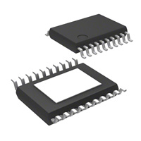
20-Pin TSSOP PowerPAD™ (PWP) Package
Thermal Shutdown Protection
PWP PACKAGE
(TOP VIEW)
GND/HSINK
GND/HSINK
GND
NC
EN
IN
IN
NC
GND/HSINK
GND/HSINK
1
20
2
19
3
18
4
17
5
16
6
15
7
14
8
13
9
12
10
11
GND/HSINK
GND/HSINK
NC
NC
RESET
FB/NC
OUT
OUT
GND/HSINK
GND/HSINK
NC − No internal connection
description
The TPS775xx devices are designed to have a fast transient response and be stable with a 10-μF low ESR
capacitors. This combination provides high performance at a reasonable cost.
Because the PMOS device behaves as a low-value resistor, the dropout voltage is very low (typically 169 mV at an
output current of 500 mA for the TPS77533) and is directly proportional to the output current. Additionally, since the
PMOS pass element is a voltage-driven device, the quiescent current is very low and independent of output loading
(typically 85 μA over the full range of output current, 0 mA to 500 mA). These two key specifications yield a significant
improvement in operating life for battery-powered systems. This LDO family also features a sleep mode; applying
a TTL high signal to EN (enable) shuts down the regulator, reducing the quiescent current to 1 μA at TJ = 25°C.
The RESET output of the TPS775xx initiates a reset in microcomputer and microprocessor systems in the event
of an undervoltage condition. An internal comparator in the TPS775xx monitors the output voltage of the regulator
to detect an undervoltage condition on the regulated output voltage.
The TPS775xx is offered in 1.5-V, 1.6-V, 1.8-V, 2.5-V, and 3.3-V fixed-voltage versions and in an adjustable version
(programmable over the range of 1.5 V to 5.5 V for TPS77501 option. Output voltage tolerance is specified as a
maximum of 2% over line, load, and temperature ranges. The TPS775xx family is available in 20 pin TSSOP
package.
Please be aware that an important notice concerning availability, standard warranty, and use in critical applications of
Texas Instruments semiconductor products and disclaimers thereto appears at the end of this data sheet.
PowerPAD is a trademark of Texas Instruments.
Copyright © 2010, Texas Instruments Incorporated
PRODUCTION DATA information is current as of publication date.
Products conform to specifications per the terms of Texas Instruments
standard warranty. Production processing does not necessarily include
testing of all parameters.
POST OFFICE BOX 655303
• DALLAS, TEXAS 75265
1
�TPS77501-EP, TPS77515-EP, TPS77516-EP, TPS77518-EP
TPS77525-EP, TPS77533-EP WITH RESET OUTPUT
FAST-TRANSIENT-RESPONSE 500-mA LOW-DROPOUT VOLTAGE REGULATORS
�
SGLS010B − MARCH 2003 − REVISED JUNE 2010
TPS77x33
DROPOUT VOLTAGE
vs
FREE-AIR TEMPERATURE
TPS77x33
LOAD TRANSIENT RESPONSE
Δ VO − Change in
Output Voltage − mV
103
102
IO = 500 mA
101
I O − Output Current − mA
VDO − Dropout Voltage − mV
Co = 10 μF
IO = 10 mA
100
10−1
IO = 0 mA
10−2
−60 −40 −20
0
20
40
60
Co = 2x47 μF
ESR = 1/2x100 mΩ
VO = 3.3 V
VI = 4.3 V
50
0
−50
500
80 100 120 140
0
0
20
TA − Free-Air Temperature − °C
40
60
80 100 120 140 160 180 200
t − Time − μs
ORDERING INFORMATION†
TA
−55°C to 125°C
OUTPUT
VOLTAGE
(V TYP)
PACKAGE
ORDERABLE
PART NUMBER
TOP-SIDE
MARKING
3.3
TSSOP − PW
Tape and reel
TPS77533MPWPREP
77533ME
2.5
TSSOP − PW
Tape and reel
TPS77525MPWPREP
77525ME
1.8
TSSOP − PW
Tape and reel
TPS77518MPWPREP
77518ME
77516ME
1.6
TSSOP − PW
Tape and reel
TPS77516MPWPREP§
1.5
TSSOP − PW
Tape and reel
TPS77515MPWPREP
77515ME
TSSOP − PW
Tape and reel
TPS77501MPWPREP
77501ME
Adjustable‡
1.5 V to 5.5 V
†
Package drawings, standard packing quantities, thermal data, symbolization, and PCB design guidelines are available at
www.ti.com/sc/package.
‡ The TPS77501 is programmable using an external resistor divider (see application information).
§ TPS77516 is Product Preview.
2
POST OFFICE BOX 655303
• DALLAS, TEXAS 75265
�TPS77501-EP, TPS77515-EP, TPS77516-EP, TPS77518-EP
TPS77525-EP, TPS77533-EP WITH RESET OUTPUT
FAST-TRANSIENT-RESPONSE 500-mA LOW-DROPOUT VOLTAGE REGULATORS
�
SGLS010B − MARCH 2003 − REVISED JUNE 2010
6
VI
RESET
IN
16
RESET
7
IN
OUT
5
0.1 μF
EN
OUT
14
VO
13
+
GND
Co†
10 μF
3
†
See application information section for capacitor selection details.
Figure 1. Typical Application Configuration for Fixed Output Options
functional block diagram—adjustable version
IN
EN
RESET
_
+
OUT
+
_
200 ms Delay
(for RESET Option)
Vref = 1.183 V
R1
FB/NC
R2
GND
External to the device
POST OFFICE BOX 655303
• DALLAS, TEXAS 75265
3
�TPS77501-EP, TPS77515-EP, TPS77516-EP, TPS77518-EP
TPS77525-EP, TPS77533-EP WITH RESET OUTPUT
FAST-TRANSIENT-RESPONSE 500-mA LOW-DROPOUT VOLTAGE REGULATORS
SGLS010B − MARCH 2003 − REVISED JUNE 2010
functional block diagram—fixed-voltage version
IN
EN
RESET
_
+
OUT
+
_
200 ms Delay
(for RESET Option)
R1
Vref = 1.183 V
R2
GND
Terminal Functions
TSSOP Package
TERMINAL
NAME
NO.
I/O
DESCRIPTION
EN
5
I
Enable input
FB/NC
15
I
Feedback input voltage for adjustable device (no connect for fixed options)
GND
3
Regulator ground
1, 2, 9, 10, 11,
12, 19, 20
Ground/heatsink
GND/HSINK
IN
6, 7
NC
4, 8, 17, 18
OUT
RESET
4
I
Input voltage
No connect
13, 14
O
Regulated output voltage
16
O
RESET output
POST OFFICE BOX 655303
• DALLAS, TEXAS 75265
�
��
TPS77501-EP, TPS77515-EP, TPS77516-EP, TPS77518-EP
TPS77525-EP, TPS77533-EP WITH RESET OUTPUT
FAST-TRANSIENT-RESPONSE 500-mA LOW-DROPOUT VOLTAGE REGULATORS
SGLS010B − MARCH 2003 − REVISED JUNE 2010
RESET timing diagram
VI
Vres†
Vres†
t
VO
VIT +‡
VIT +‡
Threshold
Voltage
VIT −‡
Less than 5% of the
output voltage
VIT −‡
t
RESET
Output
Output
Undefined
ÎÎ
ÎÎ
ÎÎ
ÎÎ
ÎÎ
200 ms Delay
200 ms Delay
ÎÎ
ÎÎ
ÎÎ
ÎÎ
ÎÎ
Output
Undefined
t
†
Vres is the minimum input voltage for a valid RESET. The symbol Vres is not currently listed within EIA or JEDEC standards for semiconductor
symbology.
‡
VIT −Trip voltage is typically 5% lower than the output voltage (95%VO) VIT− to VIT+ is the hysteresis voltage.
POST OFFICE BOX 655303
• DALLAS, TEXAS 75265
5
�TPS77501-EP, TPS77515-EP, TPS77516-EP, TPS77518-EP
TPS77525-EP, TPS77533-EP WITH RESET OUTPUT
FAST-TRANSIENT-RESPONSE 500-mA LOW-DROPOUT VOLTAGE REGULATORS
�
SGLS010B − MARCH 2003 − REVISED JUNE 2010
absolute maximum ratings over operating free-air temperature range (unless otherwise noted)†
Input voltage range‡, VI . . . . . . . . . . . . . . . . . . . . . . . . . . . . . . . . . . . . . . . . . . . . . . . . . . . . . . . . . . . −0.3 V to 13.5 V
Voltage range at EN . . . . . . . . . . . . . . . . . . . . . . . . . . . . . . . . . . . . . . . . . . . . . . . . . . . . . . . . . . . . . . −0.3 V to 16.5 V
Maximum RESET voltage . . . . . . . . . . . . . . . . . . . . . . . . . . . . . . . . . . . . . . . . . . . . . . . . . . . . . . . . . . . . . . . . . 16.5 V
Peak output current . . . . . . . . . . . . . . . . . . . . . . . . . . . . . . . . . . . . . . . . . . . . . . . . . . . . . . . . . . . . . . Internally limited
Output voltage, VO (OUT, FB) . . . . . . . . . . . . . . . . . . . . . . . . . . . . . . . . . . . . . . . . . . . . . . . . . . . . . . . . . . . . . . . . 7 V
Continuous total power dissipation . . . . . . . . . . . . . . . . . . . . . . . . . . . . . . . . . . . . . . See dissipation rating tables
Maximum junction temperature, TJ . . . . . . . . . . . . . . . . . . . . . . . . . . . . . . . . . . . . . . . . . . . . . . . . . . . . . . . . . . 125°C
Thermal impedance, junction to ambient§, θJA . . . . . . . . . . . . . . . . . . . . . . . . . . . . . . . . . . . . . . . . . . . 32.63°C/W
Thermal impedance, junction to currentt§, θJC . . . . . . . . . . . . . . . . . . . . . . . . . . . . . . . . . . . . . . . . . . . . . . . 1.4°C/W
Storage temperature range, Tstg . . . . . . . . . . . . . . . . . . . . . . . . . . . . . . . . . . . . . . . . . . . . . . . . . . . −65°C to 150°C
ESD rating, HBM . . . . . . . . . . . . . . . . . . . . . . . . . . . . . . . . . . . . . . . . . . . . . . . . . . . . . . . . . . . . . . . . . . . . . . . . . . 2 kV
†
Stresses beyond those listed under “absolute maximum ratings” may cause permanent damage to the device. These are stress ratings only, and
functional operation of the device at these or any other conditions beyond those indicated under “recommended operating conditions” is not implied.
Exposure to absolute-maximum-rated conditions for extended periods may affect device reliability.
‡ All voltage values are with respect to network terminal ground.
§ Package thermal impedance is calculated in accordance with JESD 51-5.
Estimated Lifetime in Years
TPS77501MPWP-EP Estimated Lifetime at Elevated Temperatures
Electromigration and Wirebond Voiding Fail Modes
1000
100
Wirebond Voiding Fail Mode
10
Electromigration Fail Mode
1
115
120
125
130
135
140
145
150
Continous Tj - Junction Temperature - 5C
recommended operating conditions
MIN
Input voltage,
VI#
Output voltage range, VO
Output current, IO (see Note 1)
Operating virtual junction temperature, TJ (see Note 1)
#
MAX
UNIT
2.7
10
V
1.5
5.5
V
0
500
mA
−55
125
°C
To calculate the minimum input voltage for your maximum output current, use the following equation: VI(min) = VO(max) + VDO(max load).
NOTE 1: Continuous current and operating junction temperature are limited by internal protection circuitry, but it is not recommended that the device
operate under conditions beyond those specified in this table for extended periods of time.
6
POST OFFICE BOX 655303
• DALLAS, TEXAS 75265
�TPS77501-EP, TPS77515-EP, TPS77516-EP, TPS77518-EP
TPS77525-EP, TPS77533-EP WITH RESET OUTPUT
FAST-TRANSIENT-RESPONSE 500-mA LOW-DROPOUT VOLTAGE REGULATORS
�
SGLS010B − MARCH 2003 − REVISED JUNE 2010
electrical characteristics over recommended operating free-air temperature range,
VI = VO(typ) + 1 V, IO = 1 mA, EN = 0 V, Co = 10 μF (unless otherwise noted)
PARAMETER
TEST CONDITIONS
TPS77501
TPS77515
Output voltage (10 μA to 500 mA load)
(see Note 2)
TPS77516
TPS77518
TPS77525
TPS77533
1.5 V ≤ VO ≤ 5.5 V,
MIN
TJ = 25°C
1.5 V ≤ VO ≤ 5.5 V,
TJ = −55°C to 125°C
TJ = 25°C,
2.7 V < VIN < 10 V
TJ = −55°C to 125°C,
2.7 V < VIN < 10 V
TJ = 25°C,
2.7 V < VIN < 10 V
TJ = −55°C to 125°C,
2.7 V < VIN < 10 V
TJ = 25°C,
2.8 V < VIN < 10 V
TJ = −55°C to 125°C,
2.8 V < VIN < 10 V
TJ = 25°C,
3.5 V < VIN < 10 V
TJ = −55°C to 125°C,
3.5 V < VIN < 10 V
TJ = 25°C,
4.3 V < VIN < 10 V
TJ = −55°C to 125°C,
4.3 V < VIN < 10 V
10 μA < IO < 500 mA, TJ = 25°C
IO = 500 mA,
TJ = −55°C to 125°C
Output voltage line regulation (ΔVO/VO)
(see Notes 2 and 3)
VO + 1 V < VI ≤ 10 V,
TJ = 25°C
0.98VO
1.470
BW = 200 Hz to 100 kHz, IC = 500 mA
Co = 10 μF,
TJ = 25°C
Output current limit
VO = 0 V
1.632
TJ = 25°C, 2.7 V < VI < 10 V
EN = VI,
TJ = −55°C to 125°C
2.7 V < VI < 10 V
1.764
1.836
2.5
2.450
2.550
3.366
125
%/V
3
mV
53
μVrms
2.4
°C
1
μA
10
μA
nA
V
Low level enable input voltage
0.9
TJ = 25°C
A
150
2
Co = 10 μF,
μA
A
0.01
1.7
f = 1 KHz,
V
3.3
3.234
FB = 1.5 V
High level enable input voltage
V
1.8
1.7
EN = VI,
V
1.6
1.568
Thermal shutdown junction temperature
Power supply ripple rejection (see Note 2)
UNIT
1.530
85
Output noise voltage (TPS77518)
TPS77501
1.02VO
1.5
Load regulation
FB input current
MAX
VO
Quiescent current (GND current)
EN = 0V, (see Note 2)
Standby current
TYP
60
V
dB
NOTES: 2. Minimum IN operating voltage is 2.7 V or VO(typ) + 1 V, whichever is greater. Maximum IN voltage 10V.
3. If VO ≤ 1.8 V then VImin = 2.7 V, VImax = 10 V:
Line Reg. (mV) + ǒ%ńVǓ
V
O
100
If VO ≥ 2.5 V then VImin = VO + 1 V, VImax = 10 V:
V
Line Reg. (mV) + ǒ%ńVǓ
ǒVImax * 2.7 VǓ
O
1000
ǒVImax * ǒVO ) 1 VǓǓ
POST OFFICE BOX 655303
100
• DALLAS, TEXAS 75265
1000
7
�TPS77501-EP, TPS77515-EP, TPS77516-EP, TPS77518-EP
TPS77525-EP, TPS77533-EP WITH RESET OUTPUT
FAST-TRANSIENT-RESPONSE 500-mA LOW-DROPOUT VOLTAGE REGULATORS
�
SGLS010B − MARCH 2003 − REVISED JUNE 2010
electrical characteristics over recommended operating free-air temperature range,
VI = VO(typ) + 1 V, IO = 1 mA, EN = 0 V, Co = 10 μF (unless otherwise noted) (continued)
PARAMETER
Reset
TEST CONDITIONS
Minimum input voltage for valid RESET
IO(RESET) = 300 μA
Trip threshold voltage
VO decreasing
Hysteresis voltage
Measured at VO
Output low voltage
VI = 2.7 V,
Leakage current
V(RESET) = 5 V
MIN
TYP
MAX
UNIT
1.1
92
V
98
%VO
0.5
IO(RESET) = 1mA
0.15
%VO
0.4
V
μA
1
RESET time-out delay
200
Input current (EN)
Dropout voltage (see Note 4)
TPS77533
EN = 0 V
−1
EN = VI
−1
IO = 500 mA,
TJ = 25°C
IO = 500 mA,
TJ = −55°C to 125°C
0
ms
1
μA
A
1
169
mV
287
NOTE 4: IN voltage equals VO(typ) − 100 mV; TPS77515, TPS77516, TPS77518, and TPS77525 dropout voltage limited by input voltage range
limitations (i.e., TPS77533 input voltage needs to drop to 3.2 V for purpose of this test).
TY
PICAL CHARACTERISTICS
Table of Graphs
FIGURE
vs Output current
2, 3, 4
vs Free-air temperature
5, 6, 7
Ground current
vs Free-air temperature
8
Power supply ripple rejection
vs Frequency
9
Output spectral noise density
vs Frequency
10
Zo
Output impedance
vs Frequency
11
vs Input voltage
12
VDO
Dropout voltage
vs Free-air temperature
13
VO
Output voltage
Input voltage (min)
VO
8
vs Output voltage
14
Line transient response
15, 17
Load transient response
16, 18
Output voltage
vs Time
Equivalent series resistance (ESR)
vs Output current
POST OFFICE BOX 655303
• DALLAS, TEXAS 75265
19
21 − 24
�TPS77501-EP, TPS77515-EP, TPS77516-EP, TPS77518-EP
TPS77525-EP, TPS77533-EP WITH RESET OUTPUT
FAST-TRANSIENT-RESPONSE 500-mA LOW-DROPOUT VOLTAGE REGULATORS
�
SGLS010B − MARCH 2003 − REVISED JUNE 2010
TYPICAL CHARACTERISTICS
TPS77x33
TPS77x15
OUTPUT VOLTAGE
vs
OUTPUT CURRENT
OUTPUT VOLTAGE
vs
OUTPUT CURRENT
1.4985
3.2835
VI = 4.3 V
TA = 25°C
3.2830
VI = 2.7 V
TA = 25°C
1.4980
1.4975
VO − Output Voltage − V
VO − Output Voltage − V
3.2825
1.4970
3.2820
1.4965
3.2815
1.4960
3.2810
3.2805
1.4955
1.4950
3.2800
0
0.1
0.2
0.3
0.4
0
0.5
0.1
0.2
Figure 2
0.4
0.5
Figure 3
TPS77x25
TPS77x33
OUTPUT VOLTAGE
vs
OUTPUT CURRENT
OUTPUT VOLTAGE
vs
FREE-AIR TEMPERATURE
2.4960
3.32
VI = 3.5 V
TA = 25°C
2.4955
VI = 4.3 V
3.31
VO − Output Voltage − V
2.4950
VO − Output Voltage − V
0.3
IO − Output Current − A
IO − Output Current − A
2.4945
2.4940
2.4935
2.4930
3.30
3.29
IO = 500 mA
IO = 1 mA
3.28
3.27
3.26
2.4925
2.4920
0
0.1
0.2
0.4
0.3
0.5
3.25
−60 −40 −20
0
20
40
60
80
100 120 140
TA − Free-Air Temperature − °C
IO − Output Current − A
Figure 4
Figure 5
POST OFFICE BOX 655303
• DALLAS, TEXAS 75265
9
�TPS77501-EP, TPS77515-EP, TPS77516-EP, TPS77518-EP
TPS77525-EP, TPS77533-EP WITH RESET OUTPUT
FAST-TRANSIENT-RESPONSE 500-mA LOW-DROPOUT VOLTAGE REGULATORS
�
SGLS010B − MARCH 2003 − REVISED JUNE 2010
TYPICAL CHARACTERISTICS
TPS77x15
TPS77x25
OUTPUT VOLTAGE
vs
FREE-AIR TEMPERATURE
OUTPUT VOLTAGE
vs
FREE-AIR TEMPERATURE
1.515
2.515
VI = 3.5 V
VI = 2.7 V
2.510
VO − Output Voltage − V
VO − Output Voltage − V
1.510
1.505
1.500
IO = 500 mA
IO = 1 mA
1.495
1.490
2.505
2.500
IO = 500 mA
2.495
IO = 1 mA
2.490
2.485
1.485
−60 −40 −20
0
20
40
60
80
2.480
−60 −40
100 120 140
TA − Free-Air Temperature − °C
−20
Figure 6
TPS77xxx
60
80
100 120
TPS77x33
90
95
IO = 1 mA
85
IO = 500 mA
80
75
−60 −40 −20
0
20
40
60
80
100 120 140
PSRR − Power Supply Ripple Rejection − dB
VI = 2.7 V
Ground Current − μ A
40
POWER SUPPLY RIPPLE REJECTION
vs
FREQUENCY
100
VI = 4.3 V
Co = 10 μF
TA = 25°C
80
70
60
50
40
30
20
10
0
−10
101
TA − Free-Air Temperature − °C
102
103
104
f − Frequency − Hz
Figure 9
Figure 8
10
20
Figure 7
GROUND CURRENT
vs
FREE-AIR TEMPERATURE
90
0
TA − Free-Air Temperature − °C
POST OFFICE BOX 655303
• DALLAS, TEXAS 75265
105
106
�TPS77501-EP, TPS77515-EP, TPS77516-EP, TPS77518-EP
TPS77525-EP, TPS77533-EP WITH RESET OUTPUT
FAST-TRANSIENT-RESPONSE 500-mA LOW-DROPOUT VOLTAGE REGULATORS
�
SGLS010B − MARCH 2003 − REVISED JUNE 2010
TYPICAL CHARACTERISTICS
TPS77x33
TPS77x33
OUTPUT SPECTRAL NOISE DENSITY
vs
FREQUENCY
OUTPUT IMPEDANCE
vs
FREQUENCY
100
VI = 4.3 V
Co = 10 μF
TA = 25°C
VI = 4.3 V
Co = 10 μF
TA = 25°C
Zo − Output Impedance − Ω
Output Spectral Noise Density − μV Hz
10−5
IO = 7 mA
10−6
IO = 500 mA
10−7
10−8
102
103
104
IO = 1 mA
10−1
IO = 500 mA
10−2
101
105
102
103
104
f − Frequency − kHz
f − Frequency − Hz
Figure 10
105
106
Figure 11
TPS77x33
TPS77x01
DROPOUT VOLTAGE
vs
FREE-AIR TEMPERATURE
DROPOUT VOLTAGE
vs
INPUT VOLTAGE
103
350
IO = 500 mA
Co = 10 μF
VDO − Dropout Voltage − mV
VDO − Dropout Voltage − mV
300
250
200
TA = 25°C
TA = 125°C
150
100
TA = −40°C
102
IO = 500 mA
101
IO = 10 mA
100
10−1
50
IO = 0 mA
0
2.5
3
3.5
4
VI − Input Voltage − V
4.5
5
10−2
−60 −40 −20
0
20
40
60
80 100 120 140
TA − Free-Air Temperature − °C
Figure 12
Figure 13
POST OFFICE BOX 655303
• DALLAS, TEXAS 75265
11
�TPS77501-EP, TPS77515-EP, TPS77516-EP, TPS77518-EP
TPS77525-EP, TPS77533-EP WITH RESET OUTPUT
FAST-TRANSIENT-RESPONSE 500-mA LOW-DROPOUT VOLTAGE REGULATORS
�
SGLS010B − MARCH 2003 − REVISED JUNE 2010
TYPICAL CHARACTERISTICS
INPUT VOLTAGE (MIN)
vs
OUTPUT VOLTAGE
TPS77x15
LINE TRANSIENT RESPONSE
VI − Input Voltage − V
4
TA = 25°C
TA = 125°C
3.7
2.7
3
TA = −40°C
Δ VO − Change in
Output Voltage − mV
VI − Input Voltage (Min) − V
IO = 0.5 A
2.7
2
1.5
1.75
2
2.25 2.5 2.75
3
VO − Output Voltage − V
3.25
10
0
Co = 10 μF
TA = 25°C
−10
3.5
0
20
40
60
Figure 15
TPS77x15
TPS77x33
LOAD TRANSIENT RESPONSE
LINE TRANSIENT RESPONSE
VI − Input Voltage − V
Co = 2x47 μF
ESR = 1/2x100 mΩ
VO = 1.5 V
VIN = 2.7 V
0
−50
Co = 10 μF
TA = 25°C
5.3
4.3
Δ VO − Change in
Output Voltage − mV
I O − Output Current − mA
Δ VO − Change in
Output Voltage − mV
Figure 14
50
500
0
0
20
40
60
80 100 120 140 160 180 200
t − Time − μs
10
0
−10
0
20
40
60
80 100 120 140 160 180 200
t − Time − μs
Figure 17
Figure 16
12
80 100 120 140 160 180 200
t − Time − μs
POST OFFICE BOX 655303
• DALLAS, TEXAS 75265
�TPS77501-EP, TPS77515-EP, TPS77516-EP, TPS77518-EP
TPS77525-EP, TPS77533-EP WITH RESET OUTPUT
FAST-TRANSIENT-RESPONSE 500-mA LOW-DROPOUT VOLTAGE REGULATORS
�
SGLS010B − MARCH 2003 − REVISED JUNE 2010
TYPICAL CHARACTERISTICS
TPS77x33
OUTPUT VOLTAGE
vs
TIME (AT STARTUP)
TPS77x33
4
50
VO− Output Voltage − V
Co = 2x47 μF
ESR = 1/2x100 mΩ
VO = 3.3 V
VI = 4.3 V
0
−50
Co = 10 μF
IO = 500 mA
TA = 25°C
3
2
1
0
500
Enable Pulse − V
I O − Output Current − mA
Δ VO − Change in
Output Voltage − mV
LOAD TRANSIENT RESPONSE
0
0
20
40
60
80 100 120 140 160 180 200
t − Time − μs
0
0.1
Figure 18
VI
0.2 0.3
0.4 0.5 0.6 0.7 0.8
t − Time − ms
0.9
1
Figure 19
To Load
IN
OUT
+
EN
Co
GND
R
RL
ESR
Figure 20. Test Circuit for Typical Regions of Stability (Figures 21 through 24) (Fixed Output Options)
POST OFFICE BOX 655303
• DALLAS, TEXAS 75265
13
�TPS77501-EP, TPS77515-EP, TPS77516-EP, TPS77518-EP
TPS77525-EP, TPS77533-EP WITH RESET OUTPUT
FAST-TRANSIENT-RESPONSE 500-mA LOW-DROPOUT VOLTAGE REGULATORS
�
SGLS010B − MARCH 2003 − REVISED JUNE 2010
TYPICAL CHARACTERISTICS
TYPICAL REGION OF STABILITY
TYPICAL REGION OF STABILITY
EQUIVALENT SERIES RESISTANCE†
vs
OUTPUT CURRENT
EQUIVALENT SERIES RESISTANCE†
vs
OUTPUT CURRENT
10
ESR − Equivalent Series Resistance − Ω
ESR − Equivalent Series Resistance − Ω
10
Region of Instability
1
Region of Stability
VO = 3.3 V
Co = 4.7 μF
VI = 4.3 V
TA = 25°C
0.1
0
100
200
300
400
Region of Instability
1
Region of Stability
VO = 3.3 V
Co = 4.7 μF
VI = 4.3 V
TJ = 125°C
0.1
500
0
100
IO − Output Current − mA
Figure 21
TYPICAL REGION OF STABILITY
TYPICAL REGION OF STABILITY
EQUIVALENT SERIES RESISTANCE†
vs
OUTPUT CURRENT
500
10
ESR − Equivalent Series Resistance − Ω
ESR − Equivalent Series Resistance − Ω
400
EQUIVALENT SERIES RESISTANCE†
vs
OUTPUT CURRENT
Region of Instability
1
Region of Stability
VO = 3.3 V
Co = 22 μF
VI = 4.3 V
TA = 25°C
0.1
0
100
200
300
400
500
Region of Instability
1
Region of Stability
VO = 3.3 V
Co = 22 μF
VI = 4.3 V
TJ = 125°C
0.1
0
IO − Output Current − mA
100
200
300
400
500
IO − Output Current − mA
Figure 23
14
300
Figure 22
10
†
200
IO − Output Current − mA
Figure 24
Equivalent series resistance (ESR) refers to the total series resistance, including the ESR of the capacitor, any series resistance added
externally, and PWB trace resistance to Co.
POST OFFICE BOX 655303
• DALLAS, TEXAS 75265
��
TPS77501-EP, TPS77515-EP, TPS77516-EP, TPS77518-EP
TPS77525-EP, TPS77533-EP WITH RESET OUTPUT
FAST-TRANSIENT-RESPONSE 500-mA LOW-DROPOUT VOLTAGE REGULATORS
SGLS010B − MARCH 2003 − REVISED JUNE 2010
APPLICATION INFORMATION
The TPS775xx family includes five fixed-output voltage regulators (1.5 V, 1.6 V, 1.8 V, 2.5 V, and 3.3 V), and an
adjustable regulator, the TPS77501 (adjustable from 1.5 V to 5.5 V).
device operation
The TPS775xx feature very low quiescent current, which remains virtually constant even with varying loads.
Conventional LDO regulators use a pnp pass element, the base current of which is directly proportional to the load
current through the regulator (IB = IC/β). The TPS775xx use a PMOS transistor to pass current; because the gate
of the PMOS is voltage driven, operating current is low and invariable over the full load range.
Another pitfall associated with the pnp-pass element is its tendency to saturate when the device goes into dropout.
The resulting drop in β forces an increase in IB to maintain the load. During power up, this translates to large start-up
currents. Systems with limited supply current may fail to start up. In battery-powered systems, it means rapid battery
discharge when the voltage decays below the minimum required for regulation. The TPS775xx quiescent currents
remain low even when the regulator drops out, eliminating both problems.
The TPS775xx family also features a shutdown mode that places the output in the high-impedance state (essentially
equal to the feedback-divider resistance) and reduces quiescent current to 2 μA. If the shutdown feature is not used,
EN should be tied to ground.
minimum load requirements
The TPS775xx family is stable even at zero load; no minimum load is required for operation.
FB—pin connection (adjustable version only)
The FB pin is an input pin to sense the output voltage and close the loop for the adjustable option . The output voltage
is sensed through a resistor divider network to close the loop as it is shown in Figure 26. Normally, this connection
should be as short as possible; however, the connection can be made near a critical circuit to improve performance
at that point. Internally, FB connects to a high-impedance wide-bandwidth amplifier and noise pickup feeds through
to the regulator output. Routing the FB connection to minimize/avoid noise pickup is essential.
external capacitor requirements
An input capacitor is not usually required; however, a ceramic bypass capacitor (0.047 μF or larger) improves load
transient response and noise rejection if the TPS775xx is located more than a few inches from the power supply.
A higher-capacitance electrolytic capacitor may be necessary if large (hundreds of milliamps) load transients with
fast rise times are anticipated.
Like all low dropout regulators, the TPS775xx require an output capacitor connected between OUT and GND to
stabilize the internal control loop. The minimum recommended capacitance value is 10 μF and the ESR (equivalent
series resistance) must be between 50 mΩ and 1.5 Ω. Capacitor values 10 μF or larger are acceptable, provided
the ESR is less than 1.5 Ω. Solid tantalum electrolytic, aluminum electrolytic, and multilayer ceramic capacitors are
all suitable, provided they meet the requirements described previously.
POST OFFICE BOX 655303
• DALLAS, TEXAS 75265
15
�TPS77501-EP, TPS77515-EP, TPS77516-EP, TPS77518-EP
TPS77525-EP, TPS77533-EP WITH RESET OUTPUT
FAST-TRANSIENT-RESPONSE 500-mA LOW-DROPOUT VOLTAGE REGULATORS
�
SGLS010B − MARCH 2003 − REVISED JUNE 2010
APPLICATION INFORMATION
external capacitor requirements (continued)
6
VI
7
RESET 16
IN
250 kΩ
IN
OUT
C1
0.1 μF
5
RESET
EN
OUT
14
VO
13
Co
+
10 μF
GND
3
Figure 25. Typical Application Circuit (Fixed Versions)
programming the TPS77501 adjustable LDO regulator
The output voltage of the TPS77501 adjustable regulator is programmed using an external resistor divider as shown
in Figure 26. The output voltage is calculated using:
V
O
+V
ǒ1 ) R1
Ǔ
R2
ref
(1)
Where:
Vref = 1.1834 V typ (the internal reference voltage)
Resistors R1 and R2 should be chosen for approximately 10-μA divider current. Lower value resistors can be used
but offer no inherent advantage and waste more power. Higher values should be avoided as leakage currents at
FB increase the output voltage error. The recommended design procedure is to choose
R2 = 110 kΩ to set the divider current at approximately 10 μA and then calculate R1 using:
R1 +
ǒ
V
V
Ǔ
O *1
ref
(2)
R2
OUTPUT VOLTAGE
PROGRAMMING GUIDE
TPS77501
VI
0.1 μF
IN
RESET
250 kΩ
≥ 1.7 V
≤ 0.9 V
Reset Output
EN
OUT
VO
R1
FB / NC
GND
Co
OUTPUT
VOLTAGE
R1
121
110
kΩ
3.3 V
196
110
kΩ
3.6 V
226
110
kΩ
4.75 V
332
110
kΩ
R2
POST OFFICE BOX 655303
• DALLAS, TEXAS 75265
UNIT
2.5 V
Figure 26. TPS77501 Adjustable LDO Regulator Programming
16
R2
�TPS77501-EP, TPS77515-EP, TPS77516-EP, TPS77518-EP
TPS77525-EP, TPS77533-EP WITH RESET OUTPUT
FAST-TRANSIENT-RESPONSE 500-mA LOW-DROPOUT VOLTAGE REGULATORS
�
SGLS010B − MARCH 2003 − REVISED JUNE 2010
APPLICATION INFORMATION
reset indicator
The TPS775xx features a RESET output that can be used to monitor the status of the regulator. The internal
comparator monitors the output voltage: when the output drops to between 92% and 98% of its nominal regulated
value, the RESET output transistor turns on, taking the signal low. The open-drain output requires a pullup resistor.
If not used, it can be left floating. RESET can be used to drive power-on reset circuitry or as a low-battery indicator.
RESET does not assert itself when the regulated output voltage falls outside the specified 2% tolerance, but instead
reports an output voltage low relative to its nominal regulated value (refer to timing diagram for start-up sequence).
regulator protection
The TPS775xx PMOS-pass transistors have a built-in back diode that conducts reverse currents when the input
voltage drops below the output voltage (e.g., during power down). Current is conducted from the output to the input
and is not internally limited. When extended reverse voltage is anticipated, external limiting may be appropriate.
The TPS775xx also feature internal current limiting and thermal protection. During normal operation, the TPS775xx
limit output current to approximately 1.7 A. When current limiting engages, the output voltage scales back linearly
until the overcurrent condition ends. While current limiting is designed to prevent gross device failure, care should
be taken not to exceed the power dissipation ratings of the package. If the temperature of the device exceeds
150°C(typ), thermal-protection circuitry shuts it down. Once the device has cooled below 130°C(typ), regulator
operation resumes.
power dissipation and junction temperature
Specified regulator operation is assured to a junction temperature of 125°C; the maximum junction temperature
should be restricted to 125°C under normal operating conditions. This restriction limits the power dissipation the
regulator can handle in any given application. To ensure the junction temperature is within acceptable limits,
calculate the maximum allowable dissipation, PD(max), and the actual dissipation, PD, which must be less than or
equal to PD(max).
The maximum-power-dissipation limit is determined using the following equation:
P
T max * T
A
+ J
D(max)
R
qJA
Where:
TJmax is the maximum allowable junction temperature.
RθJA is the thermal resistance junction-to-ambient for the package, i.e., 32.6°C/W for the 20-terminal
PWP with no airflow.
TA is the ambient temperature.
The regulator dissipation is calculated using:
P
D
ǒ
Ǔ
+ V *V
I
O
I
O
Power dissipation resulting from quiescent current is negligible. Excessive power dissipation will trigger the thermal
protection circuit.
POST OFFICE BOX 655303
• DALLAS, TEXAS 75265
17
�PACKAGE OPTION ADDENDUM
www.ti.com
14-Oct-2022
PACKAGING INFORMATION
Orderable Device
Status
(1)
Package Type Package Pins Package
Drawing
Qty
Eco Plan
(2)
Lead finish/
Ball material
MSL Peak Temp
Op Temp (°C)
Device Marking
(3)
Samples
(4/5)
(6)
TPS77501MPWPREP
ACTIVE
HTSSOP
PWP
20
2000
RoHS & Green
NIPDAU
Level-2-260C-1 YEAR
-55 to 125
77501ME
Samples
TPS77515MPWPREP
ACTIVE
HTSSOP
PWP
20
2000
RoHS & Green
NIPDAU
Level-2-260C-1 YEAR
-55 to 125
77515ME
Samples
TPS77518MPWPREP
ACTIVE
HTSSOP
PWP
20
2000
RoHS & Green
NIPDAU
Level-2-260C-1 YEAR
-55 to 125
77518ME
Samples
TPS77525MPWPREP
ACTIVE
HTSSOP
PWP
20
2000
RoHS & Green
NIPDAU
Level-2-260C-1 YEAR
-55 to 125
77525ME
Samples
TPS77533MPWPREP
ACTIVE
HTSSOP
PWP
20
2000
RoHS & Green
NIPDAU
Level-2-260C-1 YEAR
-55 to 125
77533ME
Samples
V62/03631-01XE
ACTIVE
HTSSOP
PWP
20
2000
RoHS & Green
NIPDAU
Level-2-260C-1 YEAR
-55 to 125
77501ME
Samples
V62/03631-02XE
ACTIVE
HTSSOP
PWP
20
2000
RoHS & Green
NIPDAU
Level-2-260C-1 YEAR
-55 to 125
77515ME
Samples
V62/03631-04XE
ACTIVE
HTSSOP
PWP
20
2000
RoHS & Green
NIPDAU
Level-2-260C-1 YEAR
-55 to 125
77518ME
Samples
V62/03631-05XE
ACTIVE
HTSSOP
PWP
20
2000
RoHS & Green
NIPDAU
Level-2-260C-1 YEAR
-55 to 125
77525ME
Samples
V62/03631-06XE
ACTIVE
HTSSOP
PWP
20
2000
RoHS & Green
NIPDAU
Level-2-260C-1 YEAR
-55 to 125
77533ME
Samples
(1)
The marketing status values are defined as follows:
ACTIVE: Product device recommended for new designs.
LIFEBUY: TI has announced that the device will be discontinued, and a lifetime-buy period is in effect.
NRND: Not recommended for new designs. Device is in production to support existing customers, but TI does not recommend using this part in a new design.
PREVIEW: Device has been announced but is not in production. Samples may or may not be available.
OBSOLETE: TI has discontinued the production of the device.
(2)
RoHS: TI defines "RoHS" to mean semiconductor products that are compliant with the current EU RoHS requirements for all 10 RoHS substances, including the requirement that RoHS substance
do not exceed 0.1% by weight in homogeneous materials. Where designed to be soldered at high temperatures, "RoHS" products are suitable for use in specified lead-free processes. TI may
reference these types of products as "Pb-Free".
RoHS Exempt: TI defines "RoHS Exempt" to mean products that contain lead but are compliant with EU RoHS pursuant to a specific EU RoHS exemption.
Green: TI defines "Green" to mean the content of Chlorine (Cl) and Bromine (Br) based flame retardants meet JS709B low halogen requirements of


 工商网监
湘ICP备2023018690号
工商网监
湘ICP备2023018690号
