TPS781 Series
www.ti.com ........................................................................................................................................................... SBVS102B – MARCH 2008 – REVISED MAY 2008
150mA, Low-Dropout Regulator, Ultralow-Power, IQ 1µA
with Pin-Selectable, Dual-Level Output Voltage
FEATURES
1
• Low IQ: 1µA
• 150mA, Low-Dropout Regulator with
Pin-Selectable Dual Voltage Level Output
• Low Dropout: 200mV at 150mA
• 3% Accuracy Over Load/Line/Temperature
• Available in Dual-Level, Fixed Output Voltages
from 1.5V to 4.2V Using Innovative Factory
EPROM Programming
• Available in an Adjustable Version from 1.22V
to 5.25V or a Dual-Level Output Version
• VSET Pin Toggles Output Voltage Between Two
Factory-Programmed Voltage Levels
• Stable with a 1.0µF Ceramic Capacitor
• Thermal Shutdown and Overcurrent Protection
• CMOS Logic Level-Compatible Enable Pin
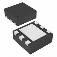
• Available in DDC (TSOT23-5) or DRV (2mm ×
2mm SON-6) Package Options
2
APPLICATIONS
•
•
•
•
TI MSP430 Attach Applications
Power Rails with Programming Mode
Dual Voltage Levels for Power-Saving Mode
Wireless Handsets, Smartphones, PDAs, MP3
Players, and Other Battery-Operated Handheld
Products
DESCRIPTION
The TPS781 family of low-dropout (LDO) regulators
offer the benefits of ultralow power (IQ = 1µA),
miniaturized packaging (2×2 SON-6), and selectable
dual-level output voltage levels. An adjustable version
is also available, but does not have the capability to
shift voltage levels.
TPS781DDC
TSOT23-5
(TOP VIEW)
IN
GND
EN
1
5
The VSET pin allows the end user to switch between
two
voltage
levels
on-the-fly
through
a
microprocessor-compatible input. This LDO is
designed specifically for battery-powered applications
where dual-level voltages are needed. With ultralow
IQ (1µA), microprocessors, memory cards, and smoke
detectors are ideal applications for this device.
The ultralow-power and selectable dual-level output
voltages allow designers to customize power
consumption for specific applications. Designers can
now shift to a lower voltage level in a battery-powered
design when the microprocessor is in sleep mode,
further reducing overall system power consumption.
The two voltage levels are preset at the factory
through a unique architecture using an EPROM. The
EPROM technique allows for numerous output
voltage options between VSET low (1.5V to 4.2V) and
VSET high (2.0V to 3.0V) in the fixed output version
only. Consult with your local factory representative for
exact voltage options and ordering information;
minimum order quantities may apply.
The TPS781 series are designed to be compatible
with the TI MSP430 and other similar products. The
enable pin is compatible with standard CMOS logic.
This LDO is stable with any output capacitor greater
than 1.0µF. Therefore, implementations of this device
require minimal board space because of miniaturized
packaging and a potentially small output capacitor.
The TPS781 series IQ (1µA) also come with thermal
shutdown and current limit to protect the device
during fault conditions. All packages have an
operating temperature range of TJ = –40°C to
+125°C. For high-performance applications requiring
a dual-level voltage option, consider the TPS780
series, with an IQ of 500nA and dynamic voltage
scaling.
TPS781DRV
2mm x 2mm SON-6
(TOP VIEW)
OUT
OUT
1
2
N/C
2
3
VSET/FB
3
4
VSET/FB
Thermal
Pad
6
IN
5
GND
4
EN
1
2
Please be aware that an important notice concerning availability, standard warranty, and use in critical applications of
Texas Instruments semiconductor products and disclaimers thereto appears at the end of this data sheet.
All trademarks are the property of their respective owners.
PRODUCTION DATA information is current as of publication date.
Products conform to specifications per the terms of the Texas
Instruments standard warranty. Production processing does not
necessarily include testing of all parameters.
Copyright © 2008, Texas Instruments Incorporated
�TPS781 Series
SBVS102B – MARCH 2008 – REVISED MAY 2008 ........................................................................................................................................................... www.ti.com
This integrated circuit can be damaged by ESD. Texas Instruments recommends that all integrated circuits be handled with
appropriate precautions. Failure to observe proper handling and installation procedures can cause damage.
ESD damage can range from subtle performance degradation to complete device failure. Precision integrated circuits may be more
susceptible to damage because very small parametric changes could cause the device not to meet its published specifications.
ORDERING INFORMATION (1) (2)
PRODUCT
VOUT
TPS781vvvxxxyyyz
(1)
(2)
(3)
(4)
VVV is the nominal output voltage for VOUT(HIGH) and corresponds to VSET pin low.
XXX is the nominal output voltage for VOUT(LOW) and corresponds to VSET pin high.
YYY is the package designator.
Z is the tape and reel quantity (R = 3000, T = 250).
Adjustable version (3) (4)
For the most current package and ordering information see the Package Option Addendum at the end of this document, or see the TI
web site at www.ti.com.
Additional output voltage combinations are available on a quick-turn basis using innovative, factory EPROM programming.
Minimum-order quantities apply; contact your sales representative for details and availability.
To order the adjustable version, use TPS78101YYYZ.
The device is either fixed voltage, dual-level VOUT, or adjustable voltage only. Device design does not permit a fixed and adjustable
output simultaneously.
ABSOLUTE MAXIMUM RATINGS (1)
At TJ = –40°C to +125°C, unless otherwise noted. All voltages are with respect to GND.
PARAMETER
TPS781 Series
UNIT
–0.3 to +6.0
V
Enable and VSET voltage range, VEN and VVSET
–0.3 to VIN + 0.3 (2)
V
Output voltage range, VOUT
–0.3 to VIN + 0.3V
V
Input voltage range, VIN
Maximum output current, IOUT
Internally limited
Output short-circuit duration
Indefinite
Total continuous power dissipation, PDISS
ESD rating
See the Dissipation Ratings table
Human body model (HBM)
2
kV
500
V
Operating junction temperature range, TJ
–40 to +125
°C
Storage temperature range, TSTG
–55 to +150
°C
(1)
(2)
Charged device model (CDM)
Stresses above these ratings may cause permanent damage. Exposure to absolute maximum conditions for extended periods may
degrade device reliability. These are stress ratings only, and functional operation of the device at these or any other conditions beyond
those specified is not implied.
VEN and VVSET absolute maximum rating are VIN + 0.3V or +6.0V, whichever is less.
DISSIPATION RATINGS
BOARD
DERATING FACTOR
ABOVE TA = +25°C
TA < +25°C
TA = +70°C
TA = +85°C
20°C/W
65°C/W
15.4mW/°C
1540mW
845mW
615mW
90°C/W
200°C/W
5.0mW/°C
500mW
275mW
200mW
RθJC
(1)
DRV
High-K (1)
DDC
High-K
(1)
2
RθJA
PACKAGE
The JEDEC high-K (2s2p) board used to derive this data was a 3-inch × 3-inch, multilayer board with 1-ounce internal power and ground
planes and 2-ounce copper traces on top and bottom of the board.
Submit Documentation Feedback
Copyright © 2008, Texas Instruments Incorporated
�TPS781 Series
www.ti.com ........................................................................................................................................................... SBVS102B – MARCH 2008 – REVISED MAY 2008
ELECTRICAL CHARACTERISTICS
Over operating temperature range (TJ = –40°C to +125°C), VIN = VOUT(NOM) + 0.5V or 2.2V, whichever is greater; IOUT =
100µA, VVSET = VEN = VIN, COUT = 1.0µF, fixed or adjustable, unless otherwise noted. Typical values at TJ = +25°C.
TPS781 Series
PARAMETER
VIN
TEST CONDITIONS
Input voltage range
DC output accuracy
TJ = +25°C, VSET = high/low
Over VIN, IOUT, VOUT + 0.5V ≤ VIN ≤ 5.5V,
temperature
0mA ≤ IOUT ≤ 150mA, VSET = high/low
MAX
UNIT
5.5
V
–2
±1
+2
%
–3.0
±2.0
+3.0
%
VFB
Internal reference (2)
(adjustable version only)
TJ = +25°C, VIN = 4.0V, IOUT = 75mA
VOUT_RANGE
Output voltage range (3) (4)
(adjustable version only)
VIN = 5.5V, IOUT = 100µA (2)
ΔVOUT/ΔVIN
Line regulation
VOUT(NOM) + 0.5V ≤ VIN ≤ 5.5V, IOUT = 5mA
–1
ΔVOUT/ΔIOUT
–2
VFB
1.216
V
5.25
V
+1
%
Load regulation
0mA ≤ IOUT ≤ 150mA
VDO
Dropout voltage (5)
VIN = 95% VOUT(NOM), IOUT = 150mA
VN
Output noise voltage
BW = 100Hz to 100kHz, VIN = 2.2V,
VOUT = 1.2V, IOUT = 1mA
VHI
VSET high (output VOUT(LOW)
selected), or EN high (enabled)
1.2
VIN
V
VLO
VSET low (output VOUT(HIGH)
selected), or EN low (disabled)
0
0.4
V
ICL
Output current limit
230
400
mA
1.0
1.3
µA
IGND
Ground pin current
+2
%
250
mV
µVRMS
86
VOUT = 0.90 × VOUT(NOM)
150
IOUT = 0mA
IOUT = 150mA
µA
8
ISHDN
Shutdown current (IGND)
VEN ≤ 0.4V, 2.2V ≤ VIN < 5.5V,
TJ = –40°C to +100°C
IVSET
VSET pin current
IEN
IFB
PSRR
18
130
nA
VEN = VVSET = 5.5V
70
nA
EN pin current
VEN = VVSET = 5.5V
40
nA
FB pin current (6)
(adjustable version only)
VIN = 5.5V, VOUT = 1.2V, IOUT = 100µA
10
nA
Power-supply rejection ratio
VIN = 4.3V,
VOUT = 3.3V,
IOUT = 150mA
f = 10Hz
40
dB
f = 100Hz
20
dB
f = 1kHz
15
dB
tTR(H→L)
VOUT transition time (high-to-low)
VOUT = 97% × VOUT(HIGH)
VOUT_LOW = 2.2V, VOUT(HIGH) = 3.3V,
IOUT = 10mA
800
µs
tTR(L→H)
VOUT transition time (low-to-high)
VOUT = 97% × VOUT(LOW)
VOUT_HIGH = 3.3V, VOUT(LOW) = 2.2V,
IOUT = 10mA
800
µs
Startup time (7)
COUT = 1.0µF, VOUT = 10% VOUT(NOM) to
VOUT = 90% VOUT(NOM)
500
µs
Shutdown time (8)
IOUT = 150mA, COUT = 1.0µF, VOUT = 2.8V,
VOUT = 90% VOUT(NOM) to VOUT = 10%
VOUT(NOM)
500 (9)
µs
Shutdown, temperature increasing
+160
°C
Reset, temperature decreasing
+140
°C
tSTR
tSHDN
(1)
(2)
(3)
(4)
(5)
(6)
(7)
(8)
(9)
TYP
2.2
Nominal
VOUT (1)
MIN
TSD
Thermal shutdown temperature
TJ
Operating junction temperature
–40
+125
°C
The output voltage for VSET = low/high is programmed at the factory.
Adjustable version only.
No VSET pin on the adjustable version.
No dynamic voltage scaling on the adjustable version.
VDO is not measured for devices with VOUT(NOM) < 2.3V because minimum VIN = 2.2V.
The TPS78101 FB pin is tied to VOUT. Adjustable version only.
Time from VEN = 1.2V to VOUT = 90% (VOUT(NOM)).
Time from VEN = 0.4V to VOUT = 10% (VOUT(NOM)).
See Shutdown in the Application Information section for more details.
Copyright © 2008, Texas Instruments Incorporated
Submit Documentation Feedback
3
�TPS781 Series
SBVS102B – MARCH 2008 – REVISED MAY 2008 ........................................................................................................................................................... www.ti.com
FUNCTIONAL BLOCK DIAGRAM
IN
OUT
Current
Limit
EPROM
EN
Bandgap
MUX
Thermal
Shutdown
Active
PullDown
(1)
VSET/FB
10kW
LOGIC
GND
(1)
Feedback pin (FB) for adjustable versions; VSET for fixed voltage versions.
PIN CONFIGURATIONS
TPS781DDC
TSOT23-5
(TOP VIEW)
TPS781DRV
2mm x 2mm SON-6
(TOP VIEW)
OUT
1
N/C
2
VSET/FB
3
6
IN
5
GND
4
EN
IN
1
GND
2
EN
3
5
OUT
4
VSET/FB
Thermal
Pad
(1)
(1) It is recommended that the SON package thermal pad be connected to ground.
Table 1. TERMINAL FUNCTIONS
TERMINAL
4
NAME
DRV
DDC
OUT
1
5
Regulated output voltage pin. A small (1µF) ceramic capacitor is needed from this pin to
ground to assure stability. See the Input and Output Capacitor Requirements in the
Application Information section for more details.
N/C
2
—
Not connected.
VSET/FB
3
4
Feedback pin (FB) for adjustable versions; VSET for fixed voltage versions. Driving the select
pin (VSET) below 0.4V selects preset output voltage high. Driving the VSET pin over 1.2V
selects preset output voltage low.
EN
4
3
Driving the enable pin (EN) over 1.2V turns on the regulator. Driving this pin below 0.4V puts
the regulator into shutdown mode, reducing operating current to 18nA typical.
GND
5
2
Ground pin.
IN
6
1
Input pin. A small capacitor is needed from this pin to ground to assure stability. Typical input
capacitor = 1.0µF. Both input and output capacitor grounds should be tied back to the IC
ground with no significant impedance between them.
Thermal pad
Thermal pad
—
It is recommended that the SON package thermal pad be connected to ground.
Submit Documentation Feedback
DESCRIPTION
Copyright © 2008, Texas Instruments Incorporated
�TPS781 Series
www.ti.com ........................................................................................................................................................... SBVS102B – MARCH 2008 – REVISED MAY 2008
TYPICAL CHARACTERISTICS
Over the operating temperature range of TJ = –40°C to +125°C, VIN = VOUT(TYP) + 0.5V or 2.2V, whichever is greater;
IOUT = 100µA, VEN = VVSET = VIN, COUT = 1µF, and CIN = 1µF, unless otherwise noted.
LINE REGULATION
IOUT = 5mA, VOUT = 1.22V (typ)
TPS78101
LINE REGULATION
IOUT = 5mA, VVSET = 1.2V, VOUT = 2.2V (typ)
TPS781330220
0.3
1.0
0.8
0.2
0.6
VOUT (%)
VOUT (%)
TJ = +25°C
TJ = +125°C
0
-0.1
TJ = +25°C
TJ = +85°C
0.4
0.1
TJ = -40°C
0.2
0
-0.2
TJ = +125°C
-0.4
-0.6
-0.2
TJ = +85°C
TJ = -40°C
-0.8
-0.3
-1.0
2.2
2.7
3.2
3.7
4.2
VIN (V)
4.7
5.2
5.7
2.7
3.2
3.7
4.2
VIN (V)
4.7
5.2
5.7
Figure 1.
Figure 2.
LINE REGULATION
IOUT = 150mA, VVSET = 1.2V, VOUT = 2.2V (typ)
TPS781330220
LINE REGULATION
IOUT = 5mA, VVSET = 0.4V, VOUT = 3.3V (typ)
TPS781330220
3
1.0
0.8
2
TJ = +25°C
0.4
TJ = +25°C
VOUT (%)
1
VOUT (%)
TJ = -40°C
0.6
TJ = -40°C
0
-1
0.2
0
-0.2
TJ = +85°C
-0.4
TJ = +85°C
-2
-0.6
-0.8
-3
-1.0
2.7
3.2
3.7
4.2
VIN (V)
4.7
5.2
5.7
3.8
4.0
4.2
4.4
4.6
4.8
VIN (V)
5.0
Figure 3.
Figure 4.
LINE REGULATION
IOUT = 150mA, VVSET = 0.4V, VOUT = 3.3V (typ)
TPS781330220
LOAD REGULATION
VOUT = 3.3V
TPS78101
5.2
5.6
1.5
3
2
1.0
TJ = +125°C
1
TJ = -40°C
VOUT (%)
VOUT (%)
5.4
0
0.5
TJ = +25°C
0
-1
-0.5
-2
TJ = +85°C
TJ = +25°C
TJ = +85°C
TJ = -40°C
-1.0
-3
3.8
4.0
4.2
4.4
4.6
4.8
VIN (V)
Figure 5.
Copyright © 2008, Texas Instruments Incorporated
5.0
5.2
5.4
5.6
0
25
50
75
IOUT (mA)
100
125
150
Figure 6.
Submit Documentation Feedback
5
�TPS781 Series
SBVS102B – MARCH 2008 – REVISED MAY 2008 ........................................................................................................................................................... www.ti.com
TYPICAL CHARACTERISTICS (continued)
Over the operating temperature range of TJ = –40°C to +125°C, VIN = VOUT(TYP) + 0.5V or 2.2V, whichever is greater;
IOUT = 100µA, VEN = VVSET = VIN, COUT = 1µF, and CIN = 1µF, unless otherwise noted.
LOAD REGULATION
VVSET = 1.2V, VIN = 2.7V, VOUT = 2.2V
TPS781330220
LOAD REGULATION
VVSET = 0.4V, VIN = 3.8V, VOUT = 3.3V
TPS781330220
3.0
3
2.5
2
2.0
TJ = -40°C
1
1.0
0.5
VOUT (%)
VOUT (%)
1.5
TJ = -40°C
0
-1
-0.5
TJ = +25°C
-1.0
TJ = +85°C
-2.0
0
25
50
-3
75
IOUT (mA)
100
125
150
0
25
50
75
IOUT (mA)
100
125
Figure 8.
DROPOUT VOLTAGE vs OUTPUT CURRENT
VOUT = 3.3V (typ), VIN = 0.95 × VOUT (typ)
TPS78101
DROPOUT VOLTAGE vs OUTPUT CURRENT
VVSET = 0.4V, VOUT = 3.3V (typ), VIN = 0.95 × VOUT (typ)
TPS781330220
250
180
TJ = +125°C
TJ = +85°C
140
200
VDO (VIN - VOUT) (mV)
160
TJ = +125°C
120
100
80
60
40
TJ = +85°C
150
100
50
TJ = -40°C
TJ = +25°C
20
TJ = -40°C
TJ = +25°C
0
0
0
25
50
75
IOUT (mA)
100
125
150
0
25
50
75
IOUT (mA)
100
125
150
Figure 9.
Figure 10.
DROPOUT VOLTAGE vs TEMPERATURE
VOUT = 3.3V (typ), VIN = 0.95 × VOUT (typ)
TPS78101
DROPOUT VOLTAGE vs TEMPERATURE
VVSET = 0.4V, VOUT = 3.3V (typ), VIN = 0.95 × VOUT (typ)
TPS781330220
250
250
200
150mA
150
100mA
100
50mA
50
VDO (VIN - VOUT) (mV)
200
150mA
150
100mA
100
50mA
50
10mA
10mA
0
0
-40 -25 -10
5
20 35 50 65
Temperature (°C)
Figure 11.
6
150
Figure 7.
200
VDO (VIN - VOUT) (mV)
TJ = +85°C
-2
TJ = +25°C
-1.5
VDO (VIN - VOUT) (mV)
0
Submit Documentation Feedback
80
95
110 125
-40 -25 -10
5
20 35 50 65
Temperature (°C)
80
95
110 125
Figure 12.
Copyright © 2008, Texas Instruments Incorporated
�TPS781 Series
www.ti.com ........................................................................................................................................................... SBVS102B – MARCH 2008 – REVISED MAY 2008
TYPICAL CHARACTERISTICS (continued)
Over the operating temperature range of TJ = –40°C to +125°C, VIN = VOUT(TYP) + 0.5V or 2.2V, whichever is greater;
IOUT = 100µA, VEN = VVSET = VIN, COUT = 1µF, and CIN = 1µF, unless otherwise noted.
GROUND PIN CURRENT vs INPUT VOLTAGE
IOUT = 50mA, VOUT = 1.22V
TPS78101
GROUND PIN CURRENT vs INPUT VOLTAGE
IOUT = 150mA, VOUT = 1.22V
TPS78101
6
8
5
TJ = +85°C
TJ = +125°C
TJ = +125°C
6
IGND (mA)
4
IGND (mA)
TJ = +85°C
7
3
2
5
4
3
TJ = +25°C
TJ = +25°C
TJ = -40°C
2
1
1
TJ = -40°C
0
0
2.2
2.7
3.2
3.7
4.2
VIN (V)
4.7
5.2
5.7
2.2
2.7
3.2
3.7
4.2
VIN (V)
4.7
5.2
Figure 13.
Figure 14.
GROUND PIN CURRENT vs INPUT VOLTAGE
IOUT = 50mA, VVSET = 1.2V, VOUT = 2.2V
TPS781330220
GROUND PIN CURRENT vs INPUT VOLTAGE
IOUT = 150mA, VVSET = 1.2V, VOUT = 2.2V
TPS781330220
6
5.7
12
11
5
10
TJ = +125°C
TJ = +85°C
9
TJ = +125°C
8
IGND (mA)
IGND (mA)
4
3
2
TJ = +85°C
7
6
5
4
TJ = +25°C
3
TJ = -40°C
1
TJ = +25°C
2
TJ = -40°C
1
0
0
2.7
3.2
3.7
4.2
VIN (V)
4.7
5.2
5.7
2.7
3.2
3.7
4.2
VIN (V)
4.7
Figure 15.
Figure 16.
GROUND PIN CURRENT vs INPUT VOLTAGE
IOUT = 50mA, VVSET = 0.4V, VOUT = 3.3V
TPS781330220
GROUND PIN CURRENT vs INPUT VOLTAGE
IOUT = 150mA, VVSET = 0.4V, VOUT = 3.3V
TPS781330220
6
5.7
9
8
TJ = +85°C
TJ = +125°C
TJ = +85°C
5
TJ = +125°C
7
4
6
IGND (mA)
IGND (mA)
5.2
3
2
5
4
3
TJ = +25°C
TJ = +25°C
TJ = -40°C
2
TJ = -40°C
1
1
0
0
3.8
4.0
4.2
4.4
4.6
4.8
VIN (V)
Figure 17.
Copyright © 2008, Texas Instruments Incorporated
5.0
5.2
5.4
5.6
3.8
4.0
4.2
4.4
4.6
4.8
VIN (V)
5.0
5.2
5.4
5.6
Figure 18.
Submit Documentation Feedback
7
�TPS781 Series
SBVS102B – MARCH 2008 – REVISED MAY 2008 ........................................................................................................................................................... www.ti.com
TYPICAL CHARACTERISTICS (continued)
Over the operating temperature range of TJ = –40°C to +125°C, VIN = VOUT(TYP) + 0.5V or 2.2V, whichever is greater;
IOUT = 100µA, VEN = VVSET = VIN, COUT = 1µF, and CIN = 1µF, unless otherwise noted.
SHUTDOWN CURRENT vs INPUT VOLTAGE
IOUT = 0mA, VVSET = 0.4V
TPS78101
CURRENT LIMIT vs INPUT VOLTAGE
VOUT = 90% VOUT (typ), VOUT = 1.22V (typ)
TPS78101
60
280
270
50
TJ = -40°C
Current Limit (mA)
TJ = +85°C
IGND (nA)
40
30
TJ = +25°C
20
260
250
TJ = +25°C
240
230
220
10
0
200
2.2
2.7
3.2
3.7
4.2
VIN (V)
4.7
5.2
5.7
2.2
3.2
3.7
4.2
VIN (V)
4.7
5.2
5.7
Figure 20.
CURRENT LIMIT vs INPUT VOLTAGE
VVSET = 1.2V, VOUT = 95% VOUT (typ), VOUT = 2.2V (typ)
TPS781330220
CURRENT LIMIT vs INPUT VOLTAGE
VVSET = 0.4V, VOUT = 95% VOUT (typ), VOUT = 3.3V (typ)
TPS781330220
300
300
290
290
280
Current Limit (mA)
Current Limit (mA)
2.7
Figure 19.
280
TJ = -40°C
270
260
250
TJ = +25°C
240
TJ = +85°C
230
220
270
TJ = -40°C
260
250
TJ = +25°C
240
TJ = +85°C
230
220
TJ = +125°C
210
TJ = +125°C
210
200
200
2.7
3.2
3.7
4.2
VIN (V)
4.7
5.2
5.7
3.8
4.0
4.2
4.4
4.6
4.8
VIN (V)
5.0
5.2
5.4
Figure 21.
Figure 22.
FEEDBACK PIN CURRENT vs TEMPERATURE
IOUT = 0mA, VOUT = 1.22V
TPS78101
VSET PIN CURRENT vs INPUT VOLTAGE
IOUT = 100µA, VVSET = 1.2V, VOUT = 2.2V
TPS781330220
5
1.0
4
0.8
3
0.6
IVSET (nA)
IFB (nA)
TJ = +85°C
210
TJ = -40°C
2
TJ = +25°C
TJ = -40°C
TJ = +85°C
5.6
0.4
VIN max
0.2
1
VIN min
0
0
-40 -25 -10
5
20 35 50 65
Temperature (°C)
Figure 23.
8
Submit Documentation Feedback
80
95
110 125
2.7
3.2
3.7
4.2
VIN (V)
4.7
5.2
5.7
Figure 24.
Copyright © 2008, Texas Instruments Incorporated
�TPS781 Series
www.ti.com ........................................................................................................................................................... SBVS102B – MARCH 2008 – REVISED MAY 2008
TYPICAL CHARACTERISTICS (continued)
Over the operating temperature range of TJ = –40°C to +125°C, VIN = VOUT(TYP) + 0.5V or 2.2V, whichever is greater;
IOUT = 100µA, VEN = VVSET = VIN, COUT = 1µF, and CIN = 1µF, unless otherwise noted.
VSET PIN CURRENT vs INPUT VOLTAGE
IOUT = 100µA, VVSET = 0.4V, VOUT = 3.3V
TPS781330220
ENABLE PIN CURRENT vs INPUT VOLTAGE
IOUT = 1mA, VOUT = 1.22V
TPS78101
2.5
2.0
TJ = +125°C
1.8
2.0
1.6
1.4
IEN (nA)
IVSET (nA)
1.5
1.0
TJ = -40°C
TJ = +85°C
0.5
0.8
0.2
0
-0.5
3.8
4.0
4.2
4.4
4.6
4.8
VIN (V)
5.0
5.2
5.4
5.6
2.2
3.7
4.2
VIN (V)
4.7
5.2
ENABLE PIN CURRENT vs INPUT VOLTAGE
IOUT = 100µA, VSET = 1.2V, VOUT = 2.2V
TPS781330220
ENABLE PIN CURRENT vs INPUT VOLTAGE
IOUT = 100µA, VVSET = 0.4V, VOUT = 3.3V
TPS781330220
2.0
1.8
1.8
1.6
1.6
1.4
1.4
1.2
1.2
TJ = +85°C
0.8
3.2
Figure 26.
2.0
1.0
2.7
Figure 25.
TJ = +25°C
IEN (nA)
IEN (nA)
TJ = -40°C
TJ = +25°C
0.4
TJ = +25°C
TJ = -40°C
1.0
0.6
0.4
0.4
0.2
0.2
0
TJ = +85°C
0.8
0.6
5.7
TJ = -40°C
TJ = +25°C
0
2.7
3.2
3.7
4.2
VIN (V)
4.7
5.2
5.7
3.8
4.0
4.2
4.4
4.6
4.8
VIN (V)
5.0
5.2
5.4
Figure 27.
Figure 28.
ENABLE PIN HYSTERESIS vs TEMPERATURE
IOUT = 1mA, TPS78101
ENABLE PIN HYSTERESIS vs TEMPERATURE
IOUT = 1mA, TPS781330220
1.2
1.2
1.1
1.1
1.0
5.6
1.0
VEN On
0.9
VEN (V)
0.9
TJ = +85°C
1.0
0.6
0
VEN (V)
1.2
0.8
0.7
VEN On
0.8
0.7
VEN Off
VEN Off
0.6
0.6
0.5
0.5
0.4
0.4
-40 -25 -10
5
20 35 50 65
Temperature (°C)
Figure 29.
Copyright © 2008, Texas Instruments Incorporated
80
95
110 125
-40 -25 -10
5
20 35 50 65
Temperature (°C)
80
95
110 125
Figure 30.
Submit Documentation Feedback
9
�TPS781 Series
SBVS102B – MARCH 2008 – REVISED MAY 2008 ........................................................................................................................................................... www.ti.com
TYPICAL CHARACTERISTICS (continued)
Over the operating temperature range of TJ = –40°C to +125°C, VIN = VOUT(TYP) + 0.5V or 2.2V, whichever is greater;
IOUT = 100µA, VEN = VVSET = VIN, COUT = 1µF, and CIN = 1µF, unless otherwise noted.
%ΔVOUT vs TEMPERATURE
IOUT = 1mA, VIN = 3.8V, VOUT = 3.3V
TPS78101
%ΔVOUT vs TEMPERATURE
VVSET = 1.2V, VIN = 2.7V, VOUT = 2.2V (typ)
TPS781330220
0.4
1
0.3
0.1mA
0
%DVOUT (V)
%VOUT (V)
0.2
0.1
0
-0.1
5mA
-1
150mA
-0.2
-0.3
-0.4
-2
-40 -25 -10
5
20 35 50 65
Temperature (°C)
80
95
110 125
5
20 35 50 65
Temperature (°C)
95
110 125
Figure 32.
%ΔVOUT vs TEMPERATURE
VVSET = 0.4V, VIN = 3.8V, VOUT = 3.3V (typ)
TPS781330220
OUTPUT SPECTRAL NOISE DENSITY vs FREQUENCY
CIN = 1µF, COUT = 2.2µF, VVSET = 1.2V, VIN = 2.7V
TPS781330220
Output Spectral Noise Density (mV/ÖHz)
2
1
0.1mA
0
5mA
-1
150mA
-2
-3
-40 -25 -10
5
20 35 50 65
Temperature (°C)
80
95
100
10
150mA
109mVRMS
1
0.1
50mA
109mVRMS
0.01
1mA
108mVRMS
0.001
10
110 125
100
1k
Frequency (Hz)
10k
100k
Figure 33.
Figure 34.
RIPPLE REJECTION vs FREQUENCY
VIN = 2.7V, VOUT = 1.2V, COUT = 2.2µF
TPS78101
INPUT VOLTAGE RAMP vs OUTPUT VOLTAGE
TPS781330220
80
VIN
1mA
60
50
40
50mA
Enable
VOUT
Load Current
30
0V
20
VIN = 0.0V to 5.0V
VOUT = 3.3V
IOUT = 150mA
COUT = 10mF
Current (50mA/div)
Voltage (1V/div)
70
PSRR (dB)
80
Figure 31.
3
%DVOUT (V)
-40 -25 -10
150mA
10
0
10
100
1k
10k
100k
Frequency (Hz)
Figure 35.
10
Submit Documentation Feedback
1M
10M
Time (20ms/div)
Figure 36.
Copyright © 2008, Texas Instruments Incorporated
�TPS781 Series
www.ti.com ........................................................................................................................................................... SBVS102B – MARCH 2008 – REVISED MAY 2008
TYPICAL CHARACTERISTICS (continued)
Over the operating temperature range of TJ = –40°C to +125°C, VIN = VOUT(TYP) + 0.5V or 2.2V, whichever is greater;
IOUT = 100µA, VEN = VVSET = VIN, COUT = 1µF, and CIN = 1µF, unless otherwise noted.
OUTPUT VOLTAGE vs ENABLE (SLOW RAMP)
TPS781330220
VSET
Load Current
VIN = 5.5V
VOUT = 3.3V
IOUT = 150mA
COUT = 10mF
0A
0V
0V
VIN
Load Current
VIN = 0.0V to 5.5V
VOUT = 2.2V
IOUT = 100mA
COUT = 10mF
VOUT
Time (20ms/div)
Time (1ms/div)
Figure 37.
Figure 38.
LINE TRANSIENT RESPONSE
TPS781330220
LINE TRANSIENT RESPONSE
TPS781330220
VIN
VIN
1V/div
1V/div
VOUT
VIN = 4.0V to 4.5V
VOUT = 2.2V
IOUT = 150mA
Slew Rate = 1V/ms
Time (200ms/div)
Figure 39.
Figure 40.
LOAD TRANSIENT RESPONSE
TPS781330220
LOAD TRANSIENT RESPONSE
TPS781330220
Enable
Enable
Voltage
(100mV/div)
VIN
VOUT
VIN = 4.0V to 4.5V
VOUT = 3.3V
IOUT = 150mA
Slew Rate = 1V/ms
Time (200ms/div)
Voltage
(100mV/div)
Current (50mA/div)
VOUT
Voltage (1V/div)
Enable
Current (50mA/div)
Voltage (1V/div)
VIN
INPUT VOLTAGE vs DELAY TO OUTPUT
TPS781330220
VOUT
0A
Time (5ms/div)
Figure 41.
Copyright © 2008, Texas Instruments Incorporated
VIN = 5.5V
VOUT = 3.3V
IOUT = 0mA to 60mA
COUT = 10mF
Load
Current
Current
(20mA/div)
Load
Current
Current
(10mA/div)
VIN = 5.5V
VOUT = 3.3V
IOUT = 0mA to 10mA
COUT = 10mF
VOUT
VIN
0A
Time (2ms/div)
Figure 42.
Submit Documentation Feedback
11
�TPS781 Series
SBVS102B – MARCH 2008 – REVISED MAY 2008 ........................................................................................................................................................... www.ti.com
TYPICAL CHARACTERISTICS (continued)
Over the operating temperature range of TJ = –40°C to +125°C, VIN = VOUT(TYP) + 0.5V or 2.2V, whichever is greater;
IOUT = 100µA, VEN = VVSET = VIN, COUT = 1µF, and CIN = 1µF, unless otherwise noted.
ENABLE PIN vs OUTPUT VOLTAGE RESPONSE
AND OUTPUT CURRENT
TPS781330220
ENABLE PIN vs OUTPUT VOLTAGE DELAY
TPS781330220
VIN = 5.50V
VOUT = 3.3V
IOUT = 150mA
COUT = 10mF
0V
Voltage (1V/div)
Load Current
VIN
Enable
VOUT
Load
Current
0V
Time (1ms/div)
VIN = 5.5V
VOUT = 3.3V
IOUT = 150mA
COUT = 10mF
Current (50mA/div)
VOUT
VIN
Current (50mA/div)
Voltage (1V/div)
Enable
Time (1ms/div)
Figure 43.
Figure 44.
VSET PIN TOGGLE
TPS781330220
VSET PIN TOGGLE
TPS781330220
VOUT
VOUT
1V/div
VSET
VSET
1V/div
VIN = 5.0V
Enable = VIN
IOUT = 150mA
VOUT Transitioning from 2.2V to 3.3V
VIN = 5.0V
IOUT = 150mA
VOUT Transitioning from 3.3V to 2.2V
Time (500ms/div)
Time (500ms/div)
Figure 45.
Figure 46.
VSET PIN TOGGLE (SLOW RAMP)
TPS781330220
Current (50mA/div)
Voltage (1V/div)
VIN
VOUT
VSET
100mA
VIN = 5.5V
VOUT = 3.3V
50mA
IOUT = 150mA
to 100mA 0A
COUT = 10mF
Load Current
Time (50ms/div)
Figure 47.
12
Submit Documentation Feedback
Copyright © 2008, Texas Instruments Incorporated
�TPS781 Series
www.ti.com ........................................................................................................................................................... SBVS102B – MARCH 2008 – REVISED MAY 2008
APPLICATION INFORMATION
Programming the TPS78101 Adjustable LDO
Regulator
APPLICATION EXAMPLES
The TPS781 series of LDOs typically take less than
800µs to transition from a lower voltage of 2.2V to a
higher voltage of 3.3V under an output load of
150mA; see Figure 45. Additionally, the TPS781
series contain active pull-down circuitry that
automatically pulls charge out of the voltage capacitor
to transition the output voltage from the higher
voltage to the lower voltage, even with no load
connected.
Output
voltage
overshoots
and
undershoots are minimal under this load condition.
The TPS781 series typically take less than 800µs to
transition from VSET low (3.3V to 2.2V), or VSET high
(2.2V to 3.3V); see Figure 45 and Figure 46. Both
output states of the TPS781 series are
factory-programmable between 1.5V to 4.2V. Note
that during startup or steady-state conditions, it is
important that the EN pin and VSET pin voltages never
exceed VIN + 0.3V.
4.2V to 5.5V
VIN
2.2V to 3.3V
IN
VOUT
OUT
1mF
1m F
TPS781
On
Off
EN
(
)
Where:
VFB = 1.216V typ (the internal reference voltage)
Resistors R1 and R2 should be chosen for
approximately 1.2µA divider current. Lower value
resistors can be used for improved noise
performance, but the solution consumes more power.
Higher resistor values should be avoided as leakage
current into/out of FB across R1/R2 creates an offset
voltage that artificially increases/decreases the
feedback
voltage
and
thus
erroneously
decreases/increases VOUT. Table 2 lists several
common output voltages and resistor values. The
recommended design procedure is to choose R2 =
1MΩ to set the divider current at 1.2µA, and then
calculate R1 using Equation 2:
V
R1 = OUT - 1 ´ R2
VFB
(2)
(
VSET High = VOUT(LOW)
VSET Low = VOUT(HIGH)
The output voltage of the TPS78101 adjustable
regulator is programmed using an external resistor
divider as shown in Figure 49. The output voltage
operating range is 1.2V to 5.1V, and is calculated
using Equation 1:
R
VOUT = VFB ´ 1 + 1
R2
(1)
)
VSET
GND
VIN
IN
VOUT
OUT
1mF
1m F
Figure 48. Typical Application Circuit
The TPS781 series is also used effectively in
dynamic voltage scaling (DVS) applications. DVS
applications are required to dynamically switch
between a high operational voltage to a low standby
voltage in order to reduce power consumption.
Modern multimillion gate microprocessors fabricated
with the latest sub-micron processes save power by
transitioning to a lower voltage to reduce leakage
currents while maintaining content. This architecture
enables the microprocessor to transition quickly into
an operational state (wake up) without requiring a
reload of the states from external memory, or a
reboot.
Copyright © 2008, Texas Instruments Incorporated
R1
TPS78101
FB
EN
R2
GND
VOUT = VFB ´ (1 +
R1
)
R2
Figure 49. TPS78101 Adjustable LDO Regulator
Programming
Table 2. Output Voltage Programming Guide
OUTPUT VOLTAGE
R1
R2
1.8V
0.499MΩ
1MΩ
2.8V
1.33MΩ
1MΩ
5.0V
3.16MΩ
1MΩ
Submit Documentation Feedback
13
�TPS781 Series
SBVS102B – MARCH 2008 – REVISED MAY 2008 ........................................................................................................................................................... www.ti.com
Powering the MSP430 Microcontroller
Several versions of the TPS781 are ideal for
powering the MSP430 microcontroller. Table 3 shows
potential applications of some voltage versions.
3.0V
VIN
TPS781360200
VOUT(HIGH)
(TYP)
3.6V
VOUT(LOW)
(TYP)
2.0V
1m F
LDO
I/O
2.2V
VOUT, MIN > 2.200V
required by some
MSP430s FLASH
operation.
TPS781360300
3.6V
3.0V
VOUT, MIN > 2.700V
required by some
MSP430s FLASH
operation.
2.2V
VOUT, MIN < 3.600V
required by some
MSP430s. Allows
highest speed
operation.
The TPS781 family offers many output voltage
versions to allow designers to optimize the supply
voltage for the processing speed required of the
MSP430. This flexible architecture minimizes the
supply current consumed by the particular MSP430
application. The MSP430 total system power can be
reduced by substituting the 1µA IQ TPS781 series
LDO in place of an existing, older-technology LDO.
Additionally, DVS allows for increasing the clock
speed in active mode (MSP430 VCC = 3.6V). The
3.6V VCC reduces the MSP430 time in active mode.
In low-power mode, MSP430 system power can be
further reduced by lowering the MSP430 VCC to 2.2V
in sleep mode.
Key features of the TPS781 series are an ultralow
quiescent current (1µA), DVS, and miniaturized
packaging. The TPS781 family are available in
SON-6 and TSOT-23 packages. Figure 50 shows a
typical MSP430 circuit powered by an LDO without
DVS. Figure 51 is an MSP430 circuit using a TPS781
LDO that incorporates an integrated DVS, thus
simplifying the circuit design. In a circuit without DVS,
as Figure 50 illustrates, VCC is always at 3.0V. When
the MSP430 goes into sleep mode, VCC remains at
3.0V; if DVS is applied, VCC could be reduced in
sleep mode. In Figure 51, the TPS781 LDO with
integrated DVS maintains 3.6V VCC until a logic high
signal from the MSP430 forces VOUT to level shift
VOUT from 3.6V down to 2.2V; thus reducing power in
sleep mode.
14
Submit Documentation Feedback
VSS
APPLICATION
3.6V
3.6V
MSP430
GND
VOUT, MIN > 1.800V
required by many
MSP430s. Allows
lowest power
consumption
operation.
TPS781360220
TPS781360220
VCC
1m F
Table 3. Typical MSP430 Applications
DEVICE
VOUT
VCC = 3.0V
5mA
Active
Mode
1.6mA IQ
LPM3/Sleep Mode
Figure 50. Typical LDO without DVS
2.2V to 3.6V
VIN
VOUT
1m F
VCC
1m F
TPS781
VSET
MSP430
I/O
GND
VSS
VCC = 3.6V
VCC = 2.2V
5mA
Active
Mode
Current
700nA IQ
LPM3/Sleep Mode
Figure 51. TPS781 with Integrated DVS
The other benefit of DVS is that it allows a higher VCC
voltage on the MSP430, increasing the clock speed
and reducing the active mode dwell time.
Copyright © 2008, Texas Instruments Incorporated
�TPS781 Series
www.ti.com ........................................................................................................................................................... SBVS102B – MARCH 2008 – REVISED MAY 2008
INPUT AND OUTPUT CAPACITOR
REQUIREMENTS
Although an input capacitor is not required for
stability, it is good analog design practice to connect
a 0.1µF to 1.0µF low equivalent series resistance
(ESR) capacitor across the input supply near the
regulator. This capacitor counteracts reactive input
sources and improves transient response, noise
rejection, and ripple rejection. A higher-value
capacitor may be necessary if large, fast rise-time
load transients are anticipated, or if the device is not
located near the power source. If source impedance
is not sufficiently low, a 0.1µF input capacitor may be
necessary to ensure stability.
The TPS781 series are designed to be stable with
standard ceramic capacitors with values of 1.0µF or
larger at the output. X5R- and X7R-type capacitors
are best because they have minimal variation in value
and ESR over temperature. Maximum ESR should be
less than 1.0Ω. With tolerance and dc bias effects,
the minimum capacitance to ensure stability is 1µF.
SHUTDOWN
The enable pin (EN) is active high and is compatible
with standard and low-voltage CMOS levels. When
shutdown capability is not required, EN should be
connected to the IN pin, as shown in Figure 52.
Figure 53 shows both EN and VSET connected to IN.
The TPS781 series, with internal active output
pull-down circuitry, discharges the output to within 5%
VOUT with a time (t) shown in Equation 3:
t=3
10kW ´ RL
´ COUT
10kW + RL
Where:
RL= output load resistance
COUT = output capacitance
4.2V to 5.5V
VIN
2.2V to 3.3V
IN
1mF
TPS781
EN
VSET High = VOUT(LOW)
VSET
VSET Low = VOUT(HIGH)
GND
Figure 52. Circuit Showing EN Tied High when
Shutdown Capability is Not Required
4.2V to 5.5V
INTERNAL CURRENT LIMIT
The TPS781 is internally current-limited to protect the
regulator during fault conditions. During current limit,
the output sources a fixed amount of current that is
largely independent of output voltage. For reliable
operation, the device should not be operated in a
current limit state for extended periods of time.
The PMOS pass element in the TPS781 series has a
built-in body diode that conducts current when the
voltage at OUT exceeds the voltage at IN. This
current is not limited, so if extended reverse voltage
operation is anticipated, external limiting to 5% of
rated output current may be appropriate.
Copyright © 2008, Texas Instruments Incorporated
VOUT
OUT
1m F
BOARD LAYOUT RECOMMENDATIONS TO
IMPROVE PSRR AND NOISE PERFORMANCE
To improve ac performance (such as PSRR, output
noise, and transient response), it is recommended
that the printed circuit board (PCB) be designed with
separate ground planes for VIN and VOUT, with each
ground plane connected only at the GND pin of the
device. In addition, the ground connection for the
output capacitor should connect directly to the GND
pin of the device. High ESR capacitors may degrade
PSRR.
(3)
VIN
2.2V
IN
VOUT
OUT
1mF
1m F
TPS781
EN
VSET
GND
Figure 53. Circuit to Tie Both EN and VSET High
Submit Documentation Feedback
15
�TPS781 Series
SBVS102B – MARCH 2008 – REVISED MAY 2008 ........................................................................................................................................................... www.ti.com
DROPOUT VOLTAGE
ACTIVE VOUT PULL-DOWN
The TPS781 series use a PMOS pass transistor to
achieve low dropout. When (VIN – VOUT) is less than
the dropout voltage (VDO), the PMOS pass device is
the linear region of operation and the input-to-output
resistance is the RDS(ON) of the PMOS pass element.
VDO approximately scales with output current
because the PMOS device behaves like a resistor in
dropout. As with any linear regulator, PSRR and
transient response are degraded as (VIN – VOUT)
approaches dropout. This effect is shown in the
Typical Characteristics section. Refer to application
report SLVA207, Understanding LDO Dropout,
available for download from www.ti.com.
In the TPS781 series, the active pull-down discharges
VOUT when the device is off. However, the input
voltage must be greater than 2.2V for the active
pull-down to work.
TRANSIENT RESPONSE
MINIMUM LOAD
The TPS781 series are stable with no output load.
Traditional PMOS LDO regulators suffer from lower
loop gain at very light output loads. The TPS781
employs an innovative, low-current circuit under very
light or no-load conditions, resulting in improved
output voltage regulation performance down to zero
output current. See Figure 41 for the load transient
response.
As with any regulator, increasing the size of the
output capacitor reduces over/undershoot magnitude
but increases duration of the transient response. For
more information, see Figure 42.
16
Submit Documentation Feedback
Copyright © 2008, Texas Instruments Incorporated
�TPS781 Series
www.ti.com ........................................................................................................................................................... SBVS102B – MARCH 2008 – REVISED MAY 2008
THERMAL INFORMATION
THERMAL PROTECTION
POWER DISSIPATION
Thermal protection disables the output when the
junction temperature rises to approximately +160°C,
allowing the device to cool. Once the junction
temperature cools to approximately +140°C, the
output circuitry is enabled. Depending on power
dissipation, thermal resistance, and ambient
temperature, the thermal protection circuit may cycle
on and off again. This cycling limits the dissipation of
the regulator, protecting it from damage as a result of
overheating.
The ability to remove heat from the die is different for
each
package
type,
presenting
different
considerations in the PCB layout. The PCB area
around the device that is free of other components
moves the heat from the device to the ambient air.
Performance data for JEDEC low- and high-K boards
are given in the Dissipation Ratings table. Using
heavier copper increases the effectiveness in
removing heat from the device. The addition of plated
through-holes to heat-dissipating layers also
improves the heatsink effectiveness. Power
dissipation depends on input voltage and load
conditions. Power dissipation (PD) is equal to the
product of the output current times the voltage drop
across the output pass element (VIN to VOUT), as
shown in Equation 4:
PD = (VIN - VOUT) ´ IOUT
(4)
Any tendency to activate the thermal protection circuit
indicates excessive power dissipation or an
inadequate heatsink. For reliable operation, junction
temperature should be limited to +125°C maximum.
To estimate the margin of safety in a complete design
(including
heatsink),
increase
the
ambient
temperature until the thermal protection is triggered;
use worst-case loads and signal conditions. For good
reliability, thermal protection should trigger at least
+35°C above the maximum expected ambient
condition of your particular application. This
configuration produces a worst-case junction
temperature of +125°C at the highest expected
ambient temperature and worst-case load.
PACKAGE MOUNTING
Solder pad footprint recommendations for the
TPS781 series are available from the Texas
Instruments web site at www.ti.com through the
TPS781 series product folders.
The internal protection circuitry of the TPS781 series
has been designed to protect against overload
conditions. However, it is not intended to replace
proper heatsinking. Continuously running the TPS781
series into thermal shutdown degrades device
reliability.
Copyright © 2008, Texas Instruments Incorporated
Submit Documentation Feedback
17
�PACKAGE OPTION ADDENDUM
www.ti.com
14-Oct-2022
PACKAGING INFORMATION
Orderable Device
Status
(1)
Package Type Package Pins Package
Drawing
Qty
Eco Plan
(2)
Lead finish/
Ball material
MSL Peak Temp
Op Temp (°C)
Device Marking
(3)
Samples
(4/5)
(6)
TPS78101DDCR
ACTIVE
SOT-23-THIN
DDC
5
3000
RoHS & Green
NIPDAU
Level-2-260C-1 YEAR
-40 to 125
CEB
Samples
TPS78101DDCT
ACTIVE
SOT-23-THIN
DDC
5
250
RoHS & Green
NIPDAU
Level-2-260C-1 YEAR
-40 to 125
CEB
Samples
TPS78101DRVR
ACTIVE
WSON
DRV
6
3000
RoHS & Green
NIPDAU
Level-1-260C-UNLIM
-40 to 125
CEB
Samples
TPS78101DRVT
ACTIVE
WSON
DRV
6
250
RoHS & Green NIPDAU | NIPDAUAG
Level-1-260C-UNLIM
-40 to 125
CEB
Samples
TPS781250200DDCR
ACTIVE
SOT-23-THIN
DDC
5
3000
RoHS & Green
NIPDAU
Level-2-260C-1 YEAR
-40 to 125
SAN
Samples
TPS781250200DDCT
ACTIVE
SOT-23-THIN
DDC
5
250
RoHS & Green
NIPDAU
Level-2-260C-1 YEAR
-40 to 125
SAN
Samples
TPS781330220DDCR
ACTIVE
SOT-23-THIN
DDC
5
3000
RoHS & Green
NIPDAU
Level-2-260C-1 YEAR
-40 to 125
CED
Samples
TPS781330220DDCT
ACTIVE
SOT-23-THIN
DDC
5
250
RoHS & Green
NIPDAU
Level-2-260C-1 YEAR
-40 to 125
CED
Samples
TPS781330220DRVR
ACTIVE
WSON
DRV
6
3000
RoHS & Green NIPDAU | NIPDAUAG
Level-1-260C-UNLIM
-40 to 125
CED
Samples
TPS781330220DRVT
ACTIVE
WSON
DRV
6
250
RoHS & Green NIPDAU | NIPDAUAG
Level-1-260C-UNLIM
-40 to 125
CED
Samples
(1)
The marketing status values are defined as follows:
ACTIVE: Product device recommended for new designs.
LIFEBUY: TI has announced that the device will be discontinued, and a lifetime-buy period is in effect.
NRND: Not recommended for new designs. Device is in production to support existing customers, but TI does not recommend using this part in a new design.
PREVIEW: Device has been announced but is not in production. Samples may or may not be available.
OBSOLETE: TI has discontinued the production of the device.
(2)
RoHS: TI defines "RoHS" to mean semiconductor products that are compliant with the current EU RoHS requirements for all 10 RoHS substances, including the requirement that RoHS substance
do not exceed 0.1% by weight in homogeneous materials. Where designed to be soldered at high temperatures, "RoHS" products are suitable for use in specified lead-free processes. TI may
reference these types of products as "Pb-Free".
RoHS Exempt: TI defines "RoHS Exempt" to mean products that contain lead but are compliant with EU RoHS pursuant to a specific EU RoHS exemption.
Green: TI defines "Green" to mean the content of Chlorine (Cl) and Bromine (Br) based flame retardants meet JS709B low halogen requirements of