TPS796xx-Q1
www.ti.com
SBVS154 – MARCH 2012
Ultralow-Noise, High-PSRR, Fast, RF, 1-A
LOW-DROPOUT LINEAR REGULATORS
Check for Samples: TPS796xx-Q1
FEATURES
APPLICATIONS
•
•
•
•
•
1
23
•
•
•
•
•
•
•
•
•
Qualified for Automotive Applications
AEC-Q100 Test Guidance With the Following
Results:
– Device Temperature Grade 1: –40°C to
125°C Ambient Operating Temperature
Range
– Device HBM ESD Classification Level H2
– Device CDM ESD Classification Level C3A
1-A Low-Dropout Regulator With Enable
Available in Fixed and Adjustable (1.2 V to
5.5 V) Versions
High PSRR (53 dB at 10 kHz)
Ultralow-Noise (40 μVRMS, TPS79630-Q1)
Fast Start-Up Time (50 μs)
Stable With a 1-μF Ceramic Capacitor
Excellent Load/Line Transient Response
Very Low Dropout Voltage (250 mV at Full
Load, TPS79630-Q1)
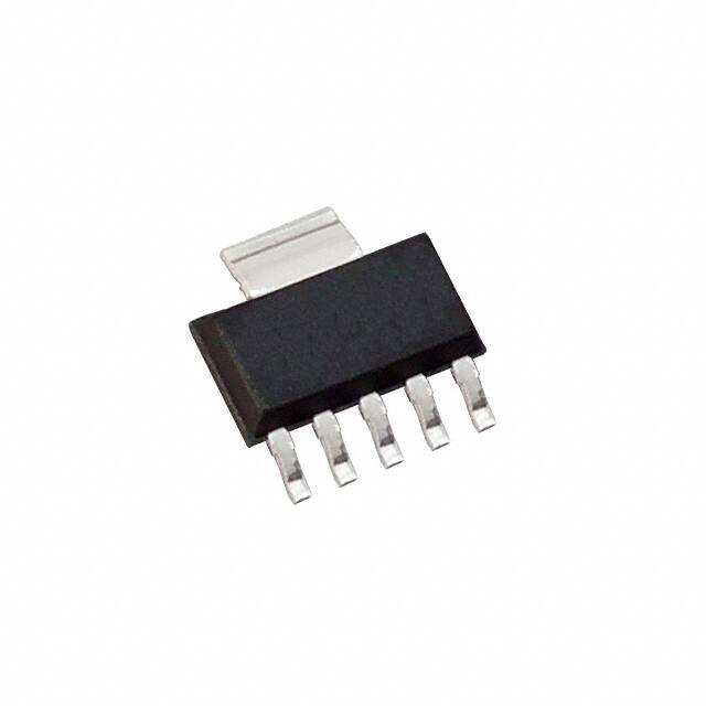
SOT223-6 Package
RF: VCOs, Receivers, ADCs
Audio
Bluetooth™, Wireless LAN
DESCRIPTION
The TPS796xx-Q1 family of low-dropout (LDO), lowpower, linear voltage regulators features high powersupply rejection ratio (PSRR), ultralow-noise, fast
start-up, and excellent line and load transient
responses in a small-outline SOT223-6 package.
Each device in the family is stable with a small 1-μF
ceramic capacitor on the output. The family uses an
advanced, proprietary BiCMOS fabrication process to
yield extremely low dropout voltages (for example,
250 mV at 1 A). Each device achieves fast start-up
times (approximately 50 μs with a 0.001-μF bypass
capacitor) while consuming very low quiescent
current (265 μA typical). Moreover, when the device
is placed in standby mode, the supply current is
reduced to less than 1 μA. The TPS79630-Q1
exhibits approximately 40 μVRMS of output voltage
noise at 3-V output, with a 0.1-μF bypass capacitor.
Applications with analog components that are noisesensitive, such as portable RF electronics, benefit
from the high-PSRR, low-noise features and the fast
response time.
TPS79630-Q1
TPS79630-Q1
RIPPLE REJECTION
vs
FREQUENCY
OUTPUT SPECTRAL NOISE DENSITY
vs
FREQUENCY
0.7
1
2
3
4
5
IOUT = 1 mA
60
6
GND
Ripple Rejection − dB
EN
IN
GND
OUT
NR/FB
70
50
VIN = 4 V
COUT = 10 mF
CNR = 0.01 mF
IOUT = 1 A
40
30
20
10
0
1
10
100
1k
10 k 100 k 1 M 10 M
Frequency (Hz)
Output Spectral Noise Density - mV/ÖHz
80
DQC PACKAGE
SOT223-6
(TOP VIEW)
VIN = 5.5 V
COUT = 2.2 mF
CNR = 0.1 mF
0.6
0.5
0.4
0.3
IOUT = 1 mA
0.2
0.1
IOUT = 1.5 A
0.0
100
1k
10 k
100 k
Frequency (Hz)
1
2
3
Please be aware that an important notice concerning availability, standard warranty, and use in critical applications of
Texas Instruments semiconductor products and disclaimers thereto appears at the end of this data sheet.
Bluetooth is a trademark of Bluetooth SIG, Inc.
All other trademarks are the property of their respective owners.
UNLESS OTHERWISE NOTED this document contains
PRODUCTION DATA information current as of publication date.
Products conform to specifications per the terms of Texas
Instruments standard warranty. Production processing does not
necessarily include testing of all parameters.
Copyright © 2012, Texas Instruments Incorporated
�TPS796xx-Q1
SBVS154 – MARCH 2012
www.ti.com
This integrated circuit can be damaged by ESD. Texas Instruments recommends that all integrated circuits be handled with
appropriate precautions. Failure to observe proper handling and installation procedures can cause damage.
ESD damage can range from subtle performance degradation to complete device failure. Precision integrated circuits may be more
susceptible to damage because very small parametric changes could cause the device not to meet its published specifications.
ORDERING INFORMATION (1)
(1)
(2)
PRODUCT
SPECIFIED
TEMPERATURE
RANGE, TA
PACKAGE TYPE,
PACKAGE
DESIGNATOR (2)
PACKAGE
MARKING
ORDERING NUMBER
TRANSPORT
MEDIA,
QUANTITY
TPS79633-Q1
–40°C to +125°C
TPS79630-Q1
–40°C to 125°C
SOT223-6, DCQ
79633Q
TPS79633QDCQRQ1
Reel, 2500
SOT223-6, DCQ
PREVIEW
TPS79630QDCQRQ1
TPS79625-Q1
Reel, 2500
–40°C to 125°C
SOT223-6, DCQ
PREVIEW
TPS79625QDCQRQ1
Reel, 2500
TPS79628-Q1
–40°C to 125°C
SOT223-6, DCQ
PREVIEW
TPS79628QDCQRQ1
Reel, 2500
For the most current package and ordering information, see the Package Option Addendum at the end of this document, or see the TI
web site at www.ti.com.
Package drawings, thermal data, and symbolization are available at www.ti.com/packaging.
ABSOLUTE MAXIMUM RATINGS (1)
Over operating temperature range (unless otherwise noted).
UNIT
VIN range
–0.3 V to 6 V
VEN range
–0.3 V to VIN + 0.3 V
VOUT range
6V
Peak output current
Internally limited
Continuous total power dissipation
See Thermal Information
table
ESD ratings
(1)
2
Human Body Model (HBM) AEC-Q100 Classification Level H2
2 kV
Charged Device Model (CDM) AEC-Q100 Classification Level C3A
500 V
Stresses beyond those listed under absolute maximum ratings may cause permanent damage to the device. These are stress ratings
only, and functional operation of the device at these or any other conditions beyond those indicated under recommended operating
conditions is not implied. Exposure to absolute-maximum-rated conditions for extended periods may affect device reliability.
Submit Documentation Feedback
Copyright © 2012, Texas Instruments Incorporated
�TPS796xx-Q1
www.ti.com
SBVS154 – MARCH 2012
RECOMMENDED OPERATING CONDITIONS
Over operating free-air temperature range (unless otherwise noted).
MIN
Ambient temperature, TA
NOM
–40°
MAX
UNIT
125
°C
THERMAL INFORMATION
TPS796xx-Q1
THERMAL METRIC
(1) (2)
DCQ
UNIT
6 PINS
θJA
Junction-to-ambient thermal resistance
θJCtop
θJB
70.4
°C/W
Junction-to-case (top) thermal resistance
70
°C/W
Junction-to-board thermal resistance
N/A
°C/W
ψJT
Junction-to-top characterization parameter
6.8
°C/W°
ψJB
Junction-to-board characterization parameter
30.1
°C/W
θJCbot
Junction-to-case (bottom) thermal resistance
6.3
°C/W
(1)
(2)
For more information about traditional and new thermal metrics, see the IC Package Thermal Metrics application report, SPRA953A.
For thermal estimates of this device based on PCB copper area, see the TI PCB Thermal Calculator.
Copyright © 2012, Texas Instruments Incorporated
Submit Documentation Feedback
3
�TPS796xx-Q1
SBVS154 – MARCH 2012
www.ti.com
ELECTRICAL CHARACTERISTICS
Over recommended operating temperature range (TA = –40°C to 125°C), VEN = VIN,, VIN = VOUT(nom) + 1 V (1), IOUT = 1 mA,
COUT = 10 μF, and CNR = 0.01 μF, unless otherwise noted. Typical values are at +25°C.
PARAMETER
TEST CONDITIONS
MIN
VIN Input voltage (1)
IOUT Continuous output current
Output
voltage
Accuracy
Fixed
VOUT < 5 V
0 μA ≤ IOUT ≤ 1 A, VOUT + 1 V ≤ VIN ≤ 5.5 V
Output voltage line regulation
(ΔVOUT%/VIN) (1)
VOUT + 1 V ≤ VIN ≤ 5.5 V
Load regulation (ΔVOUT%/ΔIOUT)
0 μA ≤ IOUT ≤ 1 A
Dropout voltage (2)
(VIN = VOUT (nom) – 0.1
V)
MAX
UNIT
5.5
V
0
1
A
–2.0
+2.0
%
0.12
%/V
0.05
5
mV
TPS79628-Q1
IOUT = 1 A
270
365
mV
TPS79630-Q1
IOUT = 1 A
250
345
mV
TPS79633-Q1
IOUT = 1 A
220
325
mV
Output current limit
VOUT = 0 V
Ground pin current
0 μA ≤ IOUT ≤ 1 A
Shutdown current (3)
VEN = 0 V, 2.7 V ≤ VIN ≤ 5.5 V
FB pin current
VFB = 1.225 V
Power-supply ripple
rejection
(1)
TYP
2.7
TPS79630-Q1
Output noise voltage (TPS79630-Q1)
Time, start-up (TPS79630-Q1)
2.4
4.2
A
265
385
μA
0.07
1
μA
1
μA
f = 100 Hz, IOUT = 10 mA
59
dB
f = 100 Hz, IOUT = 1 A
54
dB
f = 10 Hz, IOUT = 1 A
53
dB
f = 100 Hz, IOUT = 1 A
42
dB
CNR = 0.001 μF
54
μVRMS
CNR = 0.0047 μF
46
μVRMS
CNR = 0.01 μF
41
μVRMS
CNR = 0.1 μF
40
μVRMS
CNR = 0.001 μF
50
μs
CNR = 0.0047 μF
75
μs
110
μs
BW = 100 Hz to 100 kHz,
IOUT = 1 A
RL = 3 Ω, COUT = 1 μF
CNR = 0.01 μF
EN pin current
VEN = 0 V
–1
1
UVLO threshold
VCC rising
2.25
2.65
UVLO hysteresis
100
μA
V
mV
High-level enable input voltage
2.7 V ≤ VIN ≤ 5.5 V
1.7
VIN
V
Low-level enable input voltage
2.7 V ≤ VIN ≤ 5.5 V
0
0.7
V
(1)
(2)
(3)
4
Minimum VIN = VOUT + VDO or 2.7 V, whichever is greater. TPS79650-Q1 is tested at VIN = 5.5 V.
VDO is not measured for TPS79625-Q1 because minimum VIN = 2.7 V.
For adjustable version, this applies only after VIN is applied; then VEN transitions high to low.
Submit Documentation Feedback
Copyright © 2012, Texas Instruments Incorporated
�TPS796xx-Q1
www.ti.com
SBVS154 – MARCH 2012
FUNCTIONAL BLOCK DIAGRAM
IN
OUT
UVLO
Current
Sense
GND
SHUTDOWN
ILIM
_
EN
R1
+
UVLO
Thermal
Shutdown
R2
Quickstart
VIN
Bandgap
Reference
1.225 V
R2 = 40k
250 kΩ
VREF
NR
Table 1. Terminal Functions
TERMINAL
NAME
SOT223
(DCQ)
NR
5
Connecting an external capacitor to this pin bypasses noise generated by the internal bandgap. This
improves power-supply rejection and reduces output noise.
DESCRIPTION
FB
5
This terminal is the feedback input voltage for the adjustable device.
EN
1
Driving the enable pin (EN) high turns on the regulator. Driving this pin low puts the regulator into
shutdown mode. EN can be connected to IN if not used.
GND
3, Tab
IN
2
Unregulated input to the device.
OUT
4
Output of the regulator.
Regulator ground
Copyright © 2012, Texas Instruments Incorporated
Submit Documentation Feedback
5
�TPS796xx-Q1
SBVS154 – MARCH 2012
www.ti.com
TYPICAL CHARACTERISTICS
TPS79630-Q1
OUTPUT VOLTAGE
vs
OUTPUT CURRENT
TPS79628-Q1
OUTPUT VOLTAGE
vs
JUNCTION TEMPERATURE
TPS79628-Q1
GROUND CURRENT
vs
JUNCTION TEMPERATURE
2.795
4
3.05
VIN = 4 V
COUT = 10 µF
TJ = 25°C
3.04
3.03
350
VIN = 3.8 V
COUT = 10 µF
340
IOUT = 1 mA
3
2.790
3.02
330
VOUT (V)
3.00
2.99
2.98
IGND (µA)
3.01
VOUT (V)
VIN = 3.8 V
COUT = 10 µF
2
2.785
IOUT = 1 A
320
IOUT = 1 A
310
2.780
1
IOUT = 1 mA
2.97
300
2.96
2.775
0
−40 −25 −10 5
2.95
0.2
0.4
0.6
0.8
1.0
IOUT (A)
Figure 2.
Figure 3.
TPS79630-Q1
OUTPUT SPECTRAL NOISE
DENSITY
vs
FREQUENCY
TPS79630-Q1
OUTPUT SPECTRAL NOISE
DENSITY
vs
FREQUENCY
TPS79630-Q1
OUTPUT SPECTRAL NOISE
DENSITY
vs
FREQUENCY
0.6
Output Spectral Noise Density − µV//Hz
Output Spectral Noise Density − µV//Hz
6
TJ (°C)
Figure 1.
VIN = 5.5 V
COUT = 2.2 µF
CNR = 0.1 µF
0.5
0.4
0.3
IOUT = 1 mA
0.2
0.1
IOUT = 1.5 A
0.0
100
20 35 50 65 80 95 110 125
TJ (°C)
0.7
0.6
290
−40 −25 −10 5
20 35 50 65 80 95 110 125
1k
10k
100k
2.5
Output Spectral Noise Density − µV//Hz
0.0
VIN = 5.5 V
COUT = 10 µF
CNR = 0.1 µF
0.5
0.4
0.3
IOUT = 1 mA
0.2
0.1
0.0
100
IOUT = 1 A
1k
10k
100k
2.0
VIN = 5.5 V
COUT = 10 µF
IOUT = 1 A
CNR = 0.01 µF
CNR = 0.1 µF
1.5
CNR = 0.0047 µF
1.0
CNR = 0.001 µF
0.5
0.0
100
1k
10k
Frequency (Hz)
Frequency (Hz)
Frequency (Hz)
Figure 4.
Figure 5.
Figure 6.
Submit Documentation Feedback
100k
Copyright © 2012, Texas Instruments Incorporated
�TPS796xx-Q1
www.ti.com
SBVS154 – MARCH 2012
TYPICAL CHARACTERISTICS (continued)
TPS79628-Q1
DROPOUT VOLTAGE
vs
JUNCTION TEMPERATURE
80
VIN = 2.7 V
COUT = 10 µF
300
50
IOUT = 1 A
Ripple Rejection − dB
20
200
150
100
IOUT = 250 mA
COUT = 10 µF
BW = 100 Hz to 100 kHz
10
0
0.001 µF
0.0047 µF
50
30
20
10
IOUT = 250 mA
0
−40−25 −10 5 20 35 50 65 80 95 110 125
0.1 µF
0
100
1k
10k 100k
TJ (_C)
Frequency (Hz)
Figure 7.
Figure 8.
Figure 9.
TPS79630-Q1
RIPPLE REJECTION
vs
FREQUENCY
TPS79630-Q1
RIPPLE REJECTION
vs
FREQUENCY
VIN = 4 V
COUT = 10 µF
CNR = 0.1 µF
IOUT = 1 A
40
30
20
10M
START-UP TIME
VIN = 4 V
COUT = 2.2 µF
CNR = 0.01 µF
70
Ripple Rejection − dB
IOUT = 1 mA
1M
3
IOUT = 1 mA
60
VIN = 4 V,
COUT = 10 µF,
IOUT = 1.0 A
2.75
2.50
CNR =
0.0047 µF
2.25
IOUT = 1 A
40
30
Enable
CNR =
0.001 µF
2
50
VOUT (V)
70
50
10
1
CNR (µF)
80
60
IOUT = 1 A
40
50
0.01 µF
IOUT = 1 mA
60
40
30
VIN = 4 V
COUT = 10 µF
CNR = 0.01 µF
70
250
80
Ripple Rejection − dB
TPS79630-Q1
RIPPLE REJECTION
vs
FREQUENCY
350
60
VDO (mV)
RMS − Root Mean Squared Output Noise − µVRMS
TPS79630-Q1
ROOT MEAN SQUARED OUTPUT
NOISE
vs
BYPASS CAPACITANCE
1.75
1.50
CNR =
0.01 µF
1.25
1
20
10
10
0
0
0.75
0.50
0.25
100
1k
10k 100k
1M
10M
0
1
10
100
1k
10k 100k
1M
10M
200
300
400
500
600
t (ms)
Figure 10.
Figure 11.
Figure 12.
TPS79618-Q1
LINE TRANSIENT RESPONSE
TPS79630-Q1
LINE TRANSIENT RESPONSE
TPS79628-Q1
LOAD TRANSIENT RESPONSE
4
5
1
3
dv
1V
+
ms
dt
IOUT = 1 A
COUT = 10 µF
CNR = 0.01 µF
IOUT (A)
2
4
IOUT = 1 A
COUT = 10 µF
CNR = 0.01 µF
3
∆VOUT (mV)
0
−20
−40
dv
1V
+
ms
dt
150
20
0
−20
−40
20 40 60 80 100 120 140 160 180 200
t (µs)
Figure 13.
Copyright © 2012, Texas Instruments Incorporated
0
0
−1
∆VOUT (mV)
40
20
0
100
Frequency (Hz)
6
40
0
Frequency (Hz)
5
2
∆VOUT (mV)
10
VIN (V)
VIN (V)
1
20 40 60 80 100 120 140 160 180 200
t (µs)
Figure 14.
VIN = 3.8 V
COUT = 10 µF
CNR = 0.01 µF
di
1A
+
ms
dt
75
0
−75
−150
0
100 200 300 400 500 600 700 800 900 1000
t (µs)
Figure 15.
Submit Documentation Feedback
7
�TPS796xx-Q1
SBVS154 – MARCH 2012
www.ti.com
TYPICAL CHARACTERISTICS (continued)
TPS79630-Q1
DROPOUT VOLTAGE
vs
OUTPUT CURRENT
TPS79625-Q1
POWER UP/POWER DOWN
3.0
ESR − Equivalent Series Resistance − Ω
VOUT = 2.5 V
RL = 10 Ω
CNR = 0.01 µF
3.5
300
TJ = 125°C
250
2.5
VDO (mV)
2.0
200
TJ = 25°C
150
1.5
VIN
100
1.0
VOUT
0.5
TJ = −40°C
50
0
1
2
3
4
5
6
7
8
9
10
Region of
Instability
10
1
Region of Stability
0.1
1
0 100 200 300 400 500 600 700 800 9001000
10
30
60
125 250 500 750 1000
200 µs/Div
IOUT (mA)
IOUT (mA)
Figure 16.
Figure 17.
Figure 18.
TPS79630-Q1
TYPICAL REGIONS OF STABILITY EQUIVALENT SERIES
RESISTANCE (ESR)
vs
OUTPUT CURRENT
100
ESR − Equivalent Series Resistance − Ω
COUT = 1 µF
0.01
0
0
COUT = 2.2 µF
Region of
Instability
10
1
Region of Stability
0.1
0.01
TPS79630-Q1
TYPICAL REGIONS OF STABILITY EQUIVALENT SERIES
RESISTANCE (ESR)
vs
OUTPUT CURRENT
ESR − Equivalent Series Resistance − Ω
500 mV/Div
100
350
4.0
100
COUT = 10.0 µF
Region of
Instability
10
1
Region of Stability
0.1
0.01
1
8
TPS79630-Q1
TYPICAL REGIONS OF STABILITY
EQUIVALENT SERIES RESISTANCE
(ESR)
vs
OUTPUT CURRENT
10
30
60
125 250 500 750 1000
1
10
30
60
125 250 500 750 1000
IOUT (mA)
IOUT (mA)
Figure 19.
Figure 20.
Submit Documentation Feedback
Copyright © 2012, Texas Instruments Incorporated
�TPS796xx-Q1
www.ti.com
SBVS154 – MARCH 2012
APPLICATION INFORMATION
The TPS796xx-Q1 family of low-dropout (LDO) regulators has been optimized for use in noise-sensitive
equipment. The device features extremely low dropout voltages, high PSRR, ultralow output noise, low quiescent
current (265 μA typically), and enable input to reduce supply currents to less than 1 μA when the regulator is
turned off.
A typical application circuit is shown in Figure 21.
VIN
IN
VOUT
OUT
TPS796xx-Q1
2.2 mF
EN
GND
1 mF
NR
0.01 mF
Figure 21. Typical Application Circuit
External Capacitor Requirements
Although not required, it is good analog design practice to place a 0.1-μF to 2.2-μF capacitor near the input of
the regulator to counteract reactive input sources. A 2.2-μF or larger ceramic input bypass capacitor, connected
between IN and GND and located close to the TPS796xx-Q1, is required for stability and improves transient
response, noise rejection, and ripple rejection. A higher-value input capacitor may be necessary if large, fast-risetime load transients are anticipated and the device is located several inches from the power source.
As with most LDO regulators, the TPS796xx-Q1 requires an output capacitor connected between OUT and GND
to stabilize the internal control loop. The minimum recommended capacitor is 1 μF. Any 1-μF or larger ceramic
capacitor is suitable.
The internal voltage reference is a key source of noise in an LDO regulator. The TPS796xx-Q1 has an NR pin
that is connected to the voltage reference through a 250-kΩ internal resistor. The 250-kΩ internal resistor, in
conjunction with an external bypass capacitor connected to the NR pin, creates a low-pass filter to reduce the
voltage reference noise and, therefore, the noise at the regulator output. In order for the regulator to operate
properly, the current flow out of the NR pin must be at a minimum, because any leakage current creates an IR
drop across the internal resistor, thus creating an output error. Therefore, the bypass capacitor must have
minimal leakage current. The bypass capacitor should be no more than 0.1 μF in order to ensure that it is fully
charged during the quickstart time provided by the internal switch shown in the Functional Block Diagram.
For example, the TPS79630-Q1 exhibits 40 μVRMS of output voltage noise using a 0.1-μF ceramic bypass
capacitor and a 10-μF ceramic output capacitor. Note that the output starts up slower as the bypass capacitance
increases because of the RC time constant at the bypass pin that is created by the internal 250-kΩ resistor and
external capacitor.
Board Layout Recommendation to Improve PSRR and Noise Performance
To improve ac measurements such as PSRR, output noise, and transient response, it is recommended that the
board be designed with separate ground planes for VIN and VOUT, with each ground plane connected only at the
ground pin of the device. In addition, the ground connection for the bypass capacitor should connect directly to
the ground pin of the device.
Regulator Mounting
The tab of the SOT223-6 package is electrically connected to ground. For best thermal performance, the tab of
the surface-mount version should be soldered directly to the printed circuit board (PCB) copper area. Increasing
the copper area improves heat dissipation.
Solder pad footprint recommendations for the devices are presented in an application bulletin Solder Pad
Recommendations for Surface-Mount Devices, literature number AB-132, available for download from the TI web
site (www.ti.com).
Copyright © 2012, Texas Instruments Incorporated
Submit Documentation Feedback
9
�TPS796xx-Q1
SBVS154 – MARCH 2012
www.ti.com
Regulator Protection
The TPS796xx-Q1 PMOS-pass transistor has a built-in back diode that conducts reverse current when the input
voltage drops below the output voltage (for example, during power-down). Current is conducted from the output
to the input and is not internally limited. If extended reverse voltage operation is anticipated, external limiting
might be appropriate.
The TPS796xx-Q1 features internal current limiting and thermal protection. During normal operation, the
TPS796xx-Q1 limits output current to approximately 2.8 A. When current limiting engages, the output voltage
scales back linearly until the overcurrent condition ends. While current limiting is designed to prevent gross
device failure, care should be taken not to exceed the power dissipation ratings of the package. If the
temperature of the device exceeds approximately +165°C, thermal-protection circuitry shuts it down. Once the
device has cooled down to below approximately +140°C, regulator operation resumes.
10
Submit Documentation Feedback
Copyright © 2012, Texas Instruments Incorporated
�TPS796xx-Q1
www.ti.com
SBVS154 – MARCH 2012
THERMAL INFORMATION
POWER DISSIPATION
Knowing the device power dissipation and proper sizing of the thermal plane that is connected to the tab or pad
is critical to avoiding thermal shutdown and ensuring reliable operation.
Power dissipation of the device depends on input voltage and load conditions and can be calculated using
Equation 1:
P D + ǒVIN * VOUTǓ
I OUT
(1)
Power dissipation can be minimized and greater efficiency can be achieved by using the lowest possible input
voltage necessary to achieve the required output voltage regulation.
On the SON (DRB) package, the primary conduction path for heat is through the exposed pad to the PCB. The
pad can be connected to ground or be left floating; however, it should be attached to an appropriate amount of
copper PCB area to ensure the device does not overheat. On the SOT-223 (DCQ) package, the primary
conduction path for heat is through the tab to the PCB. That tab should be connected to ground. The maximum
junction-to-ambient thermal resistance depends on the maximum ambient temperature, maximum device junction
temperature, and power dissipation of the device and can be calculated using Equation 2:
()125OC * T A)
R qJA +
PD
(2)
Knowing the maximum RθJA, the minimum amount of PCB copper area needed for appropriate heatsinking can
be estimated using Figure 22.
160
DCQ
DRB
140
qJA (°C/W)
120
100
80
60
40
20
0
0
Note:
1
2
4
5
7
3
6
Board Copper Area (in2)
8
9
10
θJA value at board size of 9 in2 (that is, 3 in × 3 in) is a JEDEC standard.
Figure 22. θJA vs Board Size
Figure 22 shows the variation of θJA as a function of ground plane copper area in the board. It is intended only as
a guideline to demonstrate the effects of heat spreading in the ground plane and should not be used to estimate
actual thermal performance in real application environments.
NOTE: When the device is mounted on an application PCB, it is strongly recommended to use ΨJT and ΨJB, as
explained in the Estimating Junction Temperature section.
Copyright © 2012, Texas Instruments Incorporated
Submit Documentation Feedback
11
�TPS796xx-Q1
SBVS154 – MARCH 2012
www.ti.com
ESTIMATING JUNCTION TEMPERATURE
Using the thermal metrics ΨJT and ΨJB, as shown in the Thermal Information table, the junction temperature can
be estimated with corresponding formulas (given in Equation 3). For backwards compatibility, an older θJC,Top
parameter is listed as well.
YJT: TJ = TT + YJT · PD
YJB: TJ = TB + YJB · PD
(3)
Where PD is the power dissipation shown by Equation 2, TT is the temperature at the center-top of the IC
package, and TB is the PCB temperature measured 1 mm away from the IC package on the PCB surface (as
Figure 24 shows).
NOTE: Both TT and TB can be measured on actual application boards using a thermo-gun (an infrared
thermometer).
For more information about measuring TT and TB, see the application note SBVA025, Using New Thermal
Metrics, available for download at www.ti.com.
By looking at Figure 23, the new thermal metrics (ΨJT and ΨJB) have very little dependency on board size. That
is, using ΨJT or ΨJB with Equation 3 is a good way to estimate TJ by simply measuring TT or TB, regardless of the
application board size.
35
DCQ YJB
YJT and YJB (°C/W)
30
25
DRB YJB
20
15
10
DCQ YJT
5
DRB YJT
0
0
1
2
3
4
5
6
7
8
9
10
Board Copper Area (in2)
Figure 23. ΨJT and ΨJB vs Board Size
For a more detailed discussion of why TI does not recommend using θJC(top) to determine thermal characteristics,
refer to application report SBVA025, Using New Thermal Metrics, available for download at www.ti.com. For
further information, refer to application report SPRA953, IC Package Thermal Metrics, also available on the TI
website.
12
Submit Documentation Feedback
Copyright © 2012, Texas Instruments Incorporated
�TPS796xx-Q1
www.ti.com
SBVS154 – MARCH 2012
TB
1 mm
X
TT on top
(1)
of IC
TB on PCB
surface
(2)
TT
X
1 mm
(a) Example DRB (SON) Package Measurement
(b) Example DCQ (SOT-223) Package Measurement
(1)
TT is measured at the center of both the X- and Y-dimensional axes.
(2)
TB is measured below the package lead on the PCB surface.
Figure 24. Measuring Points for TT and TB
Copyright © 2012, Texas Instruments Incorporated
Submit Documentation Feedback
13
�PACKAGE OPTION ADDENDUM
www.ti.com
10-Dec-2020
PACKAGING INFORMATION
Orderable Device
Status
(1)
Package Type Package Pins Package
Drawing
Qty
Eco Plan
(2)
Lead finish/
Ball material
MSL Peak Temp
Op Temp (°C)
Device Marking
(3)
(4/5)
(6)
TPS79633QDCQRQ1
ACTIVE
SOT-223
DCQ
6
2500
RoHS & Green
NIPDAU
Level-3-260C-168 HR
-40 to 125
79633Q
(1)
The marketing status values are defined as follows:
ACTIVE: Product device recommended for new designs.
LIFEBUY: TI has announced that the device will be discontinued, and a lifetime-buy period is in effect.
NRND: Not recommended for new designs. Device is in production to support existing customers, but TI does not recommend using this part in a new design.
PREVIEW: Device has been announced but is not in production. Samples may or may not be available.
OBSOLETE: TI has discontinued the production of the device.
(2)
RoHS: TI defines "RoHS" to mean semiconductor products that are compliant with the current EU RoHS requirements for all 10 RoHS substances, including the requirement that RoHS substance
do not exceed 0.1% by weight in homogeneous materials. Where designed to be soldered at high temperatures, "RoHS" products are suitable for use in specified lead-free processes. TI may
reference these types of products as "Pb-Free".
RoHS Exempt: TI defines "RoHS Exempt" to mean products that contain lead but are compliant with EU RoHS pursuant to a specific EU RoHS exemption.
Green: TI defines "Green" to mean the content of Chlorine (Cl) and Bromine (Br) based flame retardants meet JS709B low halogen requirements of


 工商网监
湘ICP备2023018690号
工商网监
湘ICP备2023018690号
