��������� �
������
�� �
������
� �
��
�� ����
����� �� � ��� ��
SGLS264A − SEPTEMBER 2004 − REVISED JUNE 2008
�
���
�������� ���������
�
�������� �� ��
��
����� ����
����� ���� ����� ���� ������
The device is enabled when the applied voltage
exceeds the minimum input voltage. The usual PNP
pass transistor has been replaced by a PMOS pass
element. Because the PMOS pass element behaves as
a low-value resistor, the dropout voltage is low, typically
105 mV at 10 mA of load current and is directly
proportional to the load current. The quiescent current
is ultralow (1.2 µA typically) and is stable over the entire
range of output load current (0 mA to 10 mA). When
properly configured with a pullup resistor, the PG output
can be used to implement a power-on reset or low
battery indicator. The TPS797xx is offered in 1.8-V, 3-V,
and 3.3-V fixed options.
FEATURES
D Qualified for Automotive Applications
D 10-mA Low-Dropout Regulator
D Ultralow 1.2-µA Quiescent Current at 10 mA
D 5-Pin SC70/SOT-323 (DCK) Package
D Integrated Power Good Output
D Stable With Any Capacitor (>0.47 µF)
D Dropout Voltage Typically 105 mV at 10 mA
D
D
(TPS79733)
Over Current Limitation
−40°C to 125°C Operating Junction
Temperature Range
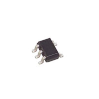
DCK PACKAGE
(TOP VIEW)
APPLICATIONS
D Battery Powered Microcontrollers and
PG
1
GND
2
NC
3
5
OUT
4
IN
Microprocessors
DESCRIPTION
TPS79733
GROUND CURRENT
vs
FREE-AIR TEMPERATURE
2
1.75
Ground Current − µ A
The TPS797xx family of low-dropout (LDO) voltage
regulators offers the benefits of low-dropout voltage and
ultralow-power operation. The device is stable with any
capacitor (>0.47 µF). Therefore, implementations of
this device require little board space due to the
miniaturized packaging and potentially small output
capacitor. In addition, the family includes an integrated
open drain active-high power good (PG) output.
Intended for use in microcontroller based,
battery-powered applications, the TPS797xx family’s
low dropout and ultralow-powered operation results in
a significant increase in system battery operating life.
The small packaging minimizes consumption of board
space.
1.50
VI = 4.3 V
VO = 3.3 V
Co = 1 µF
IO = 10 mA
1.25
1
0.75
0.50
−40
−15
10
35
60
TA − Free-Air Temperature − °C
85
Please be aware that an important notice concerning availability, standard warranty, and use in critical applications of
Texas Instruments semiconductor products and disclaimers thereto appears at the end of this data sheet.
���������� ���� ���!"�#$�!� �% &'""(�$ #% !� )'*+�&#$�!� ,#$(�"!,'&$% &!��!"� $! %)(&���&#$�!�% )(" $.( $("�% !� �(/#% ��%$"'�(�$%
%$#�,#", 0#""#�$1- �"!,'&$�!� )"!&(%%��2 ,!(% �!$ �(&(%%#"�+1 ��&+',(
$(%$��2 !� #++ )#"#�($("%-
Copyright 2008, Texas Instruments Incorporated
www.ti.com
1
���������� �
������
�� �
������
� �
SGLS264A − SEPTEMBER 2004 − REVISED JUNE 2008
TJ
AVAILABLE OPTIONS†§
VOLTAGE
PACKAGE}
PART NUMBER
1.8 V
−40°C
−40
C to 125
125°C
C
3V
SC70/SOT-323
(DCK)
3.3 V
SYMBOL
TPS79718QDCKRQ1¶
TPS79730QDCKRQ1¶
QTD
QTE
TPS79733QDCKRQ1¶
QTF
† For the most current package and ordering information, see the Package Option Addendum at the
end of this document, or see the TI web site at http://www.ti.com.
‡ Package drawings, thermal data, and symbolization are available at http://www.ti.com/packaging.
§ Contact Texas Instruments for the availability of other voltage options between 1.25 V and 4.9 V.
¶ The DCKR indicates tape and reel of 3000 parts.
absolute maximum ratings over operating free-air temperature range (unless otherwise noted)¶
Input voltage range ���� ���� �� . . . . . . . . . . . . . . . . . . . . . . . . . . . . . . . . . . . . . . . . . . . . . . . . . . . . . . . . . . −0.3 V to 6 V
Maximum dc output voltage . . . . . . . . . . . . . . . . . . . . . . . . . . . . . . . . . . . . . . . . . . . . . . . . . . . . . . . . . . . . . . . . . . . . . . 4.9 V
Peak output current . . . . . . . . . . . . . . . . . . . . . . . . . . . . . . . . . . . . . . . . . . . . . . . . . . . . . . . . . . . . . . . . . . . . Internally limited
ESD rating, HBM . . . . . . . . . . . . . . . . . . . . . . . . . . . . . . . . . . . . . . . . . . . . . . . . . . . . . . . . . . . . . . . . . . . . . . . . . . . . . . . . 3 kV
ESD rating, CDM . . . . . . . . . . . . . . . . . . . . . . . . . . . . . . . . . . . . . . . . . . . . . . . . . . . . . . . . . . . . . . . . . . . . . . . . . . . . . . . . 1 kV
Continuous total power dissipation . . . . . . . . . . . . . . . . . . . . . . . . . . . . . . . . . . . . . . . . . . See Dissipation Rating Table
Operating junction temperature range, TJ . . . . . . . . . . . . . . . . . . . . . . . . . . . . . . . . . . . . . . . . . . . . . . . . −40°C to 125°C
Operating ambient temperature range, TA . . . . . . . . . . . . . . . . . . . . . . . . . . . . . . . . . . . . . . . . . . . . . . . . −40°C to 125°C
Storage temperature range, Tstg . . . . . . . . . . . . . . . . . . . . . . . . . . . . . . . . . . . . . . . . . . . . . . . . . . . . . . . . −65°C to 150°C
¶ Stresses beyond those listed under “absolute maximum ratings” may cause permanent damage to the device. These are stress ratings only, and
functional operation of the device at these or any other conditions beyond those indicated under “recommended operating conditions” is not
implied. Exposure to absolute-maximum-rated conditions for extended periods may affect device reliability.
NOTE 1: All voltage values are with respect to network ground terminal.
DISSIPATION RATING TABLE
TA ≤ 25°C
POWER RATING
TA = 70°C
POWER RATING
TA = 85°C
POWER RATING
2.52 mW/°C
252mW
139 mW
101 mW
3.18 mW/°C
318 mW
175 mW
BOARD
PACKAGE
RθJC
°C/W
RθJA
°C/W
DERATING FACTOR
ABOVE TA = 25°C
Low K#
High K||
DCK
165.39
396.24
DCK
165.39
314.74
127 mW
# The JEDEC Low K (1s) board design used to derive this data was a 3 inch x 3 inch, two layer board with 2 ounce copper traces on top of the board.
|| The JEDEC High K (2s2p) board design used to derive this data was a 3 inch x 3 inch, multilayer board with 1 ounce internal power and ground
planes and 2 ounce copper traces on top and bottom of the board.
2
www.ti.com
���������� �
������
�� �
������
� �
SGLS264A − SEPTEMBER 2004 − REVISED JUNE 2008
electrical characteristics over recommended operating free-air temperature range,
VI = VO(typ) + 1 V, IO = 1 mA, Co = 1 µF (unless otherwise noted)
PARAMETER
VI
Input voltage (see Note 2)
IO
TJ
Operating junction temperature, TJ
TEST CONDITIONS
IO = 3 mA
IO = 10 mA
Continuous output current (see Note 3)
Output voltage (10 µA to 10 mA Load)
(see Note 4)
TPS79718
TA = 25°C,
TJ = −40°C to 125°C,
2.8 V < VI < 5.5 V
TPS79730
TA = 25°C,
TJ = −40°C to 125°C,
4 V < VI < 5.5 V
TPS79733
TA = 25°C,
TJ = −40°C to 125°C,
4.3 V < VI < 5.5 V
TA = 25°C,
TJ = −40°C to 125°C,
0 µA < IO < 10 mA
Quiescent current (GND current) (see Note 4)
Load regulation
Output voltage line regulation (∆VO/VO) (see Note 4)
Output noise voltage (TPS79718)
Output current limit
PG output low voltage
PG leakage current
4.3 V < VI < 5.5 V
MAX
UNIT
1.8
5.5
V
2
5.5
V
0
10
mA
-40
125
°C
1.8
1.71
1.89
V
3
2.880
3.12
V
3.3
3.168
3.432
1.2
IO = 10 mA
IO = 1 µA to 10 mA
5
TA = 25°C,
VO + 1 V < VI ≤ 5.5 V, TA = 25°C
VO + 1 V < VI ≤ 5.5 V, TJ = −40°C to 125°C
17
0.15
BW = 200 Hz to 100 kHz, Co = 10 µF,
IO = 10 mA,
TA = 25°C
600
190
Co = 10 µF,
TA = 25°C
50
IO = 10 mA,
IO = 10 mA,
TA = 25°C
TJ = −40°C to 125°C
110
TPS79730
TA = 25°C
TJ = −40°C to 125°C
105
TPS79733
IO = 10 mA,
IO = 10 mA,
IO(PG) = 100µA,
VO decreasing
V(PG) ≥ 0.8 V
1.2
VI = 1.4 V,
V(PG) = 5 V
IO(PG) = 100 µA
V
µA
A
mV
0.8
See Note 4
Dropout voltage (see Note 5)
PG trip threshold voltage
4 V < VI < 5.5 V
TYP
VO = 0 V,
f = 100 Hz,
IO = 10 mA,
Power supply ripple rejection (TPS79718)
Minimum input voltage for valid PG
2.8 V < VI < 5.5 V
MIN
%/V
µVRMS
300
mA
dB
400
mV
400
82
0.1
V
90
96
0.14
0.4
%VO
V
nA
NOTES: 2. To calculate the minimum input voltage for your maximum output current, use the following formula:
VI(min) = VO(max) + VDO (max load)
3. Continuous output current is limited by internal protection circuitry, but it is not recommended that the device operate under
conditions beyond those specified in this table for extended periods of time.
4. The minimum IN operating voltage is 1.8 V or VO (typ) + 1 V, whichever is greater. The maximum IN voltage is 5.5 V. There is no
minimum output current requirement and the maximum output current is 10 mA.
5. IN voltage equals VO(typ) −100 mV; The TPS79730 input voltage is set to 2.9 V and the TPS79733 input voltage is set to 3.2 V. The
TPS79718 dropout voltage is limited by input voltage range limitations.
www.ti.com
3
���������� �
������
�� �
������
� �
SGLS264A − SEPTEMBER 2004 − REVISED JUNE 2008
functional block diagram
VOUT
VIN
Current
Sense
ILIM
_
R1
+
GND
R2
Bandgap
Reference
VIN
Vref = 1.235 V
PG
Delay
Terminal Functions
TERMINAL
NAME
NO.
I/O
DESCRIPTION
GND
2
NC
3
OUT
5
O
The OUT terminal provides the regulated output voltage of the device.
PG
1
O
The PG terminal for the fixed voltage option devices is an open drain, active-high output that indicates the status
of VO (output of the LDO). When VO exceeds approximately 90% of the regulated voltage, PG goes to a high
impedance state. It goes to a low-impedance state when VO falls below approximately 90% (i.e. overload condition)
of the regulated voltage. The open drain output of the PG terminal requires a pullup resistor.
IN
4
I
The IN terminal is the power supply input to the device.
4
Ground
No connection
www.ti.com
���������� �
������
�� �
������
� �
SGLS264A − SEPTEMBER 2004 − REVISED JUNE 2008
TPS797xx PG timing diagram
VIN
Vmin
(see Note A)
t
VOUT
Threshold
Voltage
VIT −
(see Note B)
VIT +
(see Note B)
t
PG
Output
t
NOTES: A. Vmin = VOUT + VDO
B. The PG trip voltage is typically 10% lower than the output voltage (90%VO). VIT− to VIT+ is the hysteresis voltage.
www.ti.com
5
���������� �
������
�� �
������
� �
SGLS264A − SEPTEMBER 2004 − REVISED JUNE 2008
TYPICAL CHARACTERISTICS
TPS79733
TPS79718
TPS79733
OUTPUT VOLTAGE
vs
OUTPUT CURRENT
OUTPUT VOLTAGE
vs
OUTPUT CURRENT
OUTPUT VOLTAGE
vs
FREE-AIR TEMPERATURE
VI = 4.3 V
Co = 1 µF
TA = 25°C
VI = 2.8 V
Co = 1 µF
TA = 25°C
3.305
3.300
3.295
3.33
1.805
1.800
1.795
1.790
3.290
VI = 4.3 V
Co = 1 µF
3.34
V O − Output Voltage − V
1.810
V O − Output Voltage − V
3.310
V O − Output Voltage − V
3.35
1.815
3.315
3.32
3.31
IO = 1 mA
3.30
3.29
IO = 10 mA
3.28
3.27
3.26
1.785
3.285
0
2
4
6
8
IO − Output Current − mA
3.25
0
10
2
4
6
8
IO − Output Current − mA
−15
10
35
60
TA − Free-Air Temperature − °C
85
Figure 3
Figure 2
Figure 1
TPS79718
TPS79733
TPS79718
OUTPUT VOLTAGE
vs
FREE-AIR TEMPERATURE
GROUND CURRENT
vs
FREE-AIR TEMPERATURE
OUTPUT SPECTRAL NOISE DENSITY
vs
FREQUENCY
Ground Current − µ A
1.75
1.81
IO = 1 mA
1.80
IO = 10 mA
1.79
1.50
VI = 4.3 V
VO = 3.3 V
Co = 1 µF
IO = 10 mA
Output Spectral Noise Density − nV/
VI = 2.8 V
Co = 1 µF
Hz
2
1.82
V O − Output Voltage − V
−40
10
1.25
1
0.75
1.78
−40
−15
10
35
60
TA − Free-Air Temperature − °C
85
0.50
−40
VI = 2.8 V
VO = 1.8 V
Co = 1 µF
8
IO = 10 mA
6
IO = 1 mA
4
2
0
85
−15
10
35
60
TA − Free-Air Temperature − °C
10
100
1k
10 k
f − Frequency − Hz
Figure 5
Figure 4
100 k
Figure 6
TPS79733
DROPOUT VOLTAGE
vs
FREE-AIR TEMPERATURE
OUTPUT IMPEDANCE
vs
FREQUENCY
IO = 1 mA
25
20
IO = 10 mA
15
10
120
7
VI = 3.2 V
Co = 1 µF
100
IO = 10 mA
80
60
40
5
VI
4
3
VO
2
1
IO = 1 mA
20
5
VO = 3.3 V
RL = 330 Ω
6
V − Output Voltage − V
O
V − Input Voltage − V
I
Zo − Output Impedance −Ω
30
V DO − Dropout Voltage − mV
VI = 4.3 V
VO = 3.3 V
Co = 1 µF
TJ = 25°C
35
0
0
10
100
1k
10k
100k
f − Frequency − Hz
Figure 7
6
POWER UP / POWER DOWN
140
40
1M
10 M
0
−40 −25
−10
5
20
35
50
TA − Free-Air Temperature − °C
Figure 8
www.ti.com
65
80
0
10 20
30 40 50
60 70 80 90 100
t − Time − ms
Figure 9
���������� �
������
�� �
������
� �
SGLS264A − SEPTEMBER 2004 − REVISED JUNE 2008
TPS79718
TPS79718
LINE TRANSIENT RESPONSE
LOAD TRANSIENT RESPONSE
∆ V − Change In
O
Output Voltage − mV
dv
0.14 V
=
dt
µs
3.8
2.8
50
Current Load − mA
IO = 10 mA
VO = 1.8 V
Co = 4.7 µF
100
0
50
−100
100
50
0
−50
VI = 2.8 V
VO = 1.8 V
Co = 4.7 µF
−100
10
5
1 mA
0
0 100 200 300 400 500 600 700 800 900 1 k
0 200 400 600 800 1 k 12
t − Time − µs
Figure 10
18
TPS79733
TPS79733
LINE TRANSIENT RESPONSE
LOAD TRANSIENT RESPONSE
VI = 4.3 V
Co = 4.7 µF
IO = 10 mA
Co = 4.7 µF
5.3
2k
Figure 11
100
50
0
4.3
I O − Output Current − mA
V − Output Voltage − mV V − Input Voltage − V
O
I
14 16
t − Time − µs
dv
0.14 V
=
dt
µs
200
−50
−100
10
100
0
−100
−200
5
1 mA
0
0
0 100 200 300 400 500 600 700 800 900 1 k
∆ V − Change In
O
Output Voltage − mV
V − Output Voltage − mV V − Input Voltage − V
O
I
TYPICAL CHARACTERISTICS
200 400 600 800 1 k 12 14
16 18
2k
t − Time − µs
t − Time − µs
Figure 12
Figure 13
www.ti.com
7
���������� �
������
�� �
������
� �
SGLS264A − SEPTEMBER 2004 − REVISED JUNE 2008
APPLICATION INFORMATION
The TPS797xx family of low-dropout (LDO) regulators have been optimized for use in micropower applications.
They feature extremely low dropout voltages and ultralow quiescent current (1.2 µA typically).
A typical application circuit is shown in Figure 14.
TPS797xx
4
IN
PG 1
100 kΩ
+
C1
0.1 µF
−
OUT
5
VO
3
NC
GND
+
0.47 µF
2
Figure 14. Typical Application Circuit
external capacitor requirements
Although not required, a 0.1-µF or larger input bypass capacitor, connected between IN and GND and located
close to the TPS797xx, is recommended, especially when a highly resistive power supply is powering the LDO
in addition to other devices.
Like all low-dropout regulators, the TPS797xx requires an output capacitor connected between OUT and GND
to stabilize the internal control loop. The minimum recommended capacitance is 0.47 µF. Any 0.47-µF capacitor
is suitable. Capacitor values larger than 0.47 µF are acceptable.
8
www.ti.com
���������� �
������
�� �
������
� �
SGLS264A − SEPTEMBER 2004 − REVISED JUNE 2008
APPLICATION INFORMATION
power dissipation and junction temperature
Specified regulator operation is assured to a junction temperature of 125°C; restrict the maximum junction
temperature to 125°C under normal operating conditions. This restriction limits the power dissipation the
regulator can handle in any given application. To ensure the junction temperature is within acceptable limits,
calculate the maximum allowable dissipation, PD(max), and the actual dissipation, PD, which must be less than
or equal to PD(max).
The maximum-power-dissipation limit is determined using the following equation:
P
D(max)
T max * T
A
+ J
R
θJA
Where:
TJmax is the maximum allowable junction temperature.
RθJA is the thermal resistance junction-to-ambient for the package (see Power Dissipation Rating Table).
TA is the ambient temperature.
The regulator dissipation is calculated using:
P
D
ǒ
Ǔ
+ V *V
I
O
I
O
Power dissipation resulting from quiescent current is negligible. Excessive power dissipation triggers the
thermal protection circuit.
regulator protection
The TPS797xx PMOS-pass transistor has a built-in back diode that conducts reverse current when the input
voltage drops below the output voltage (e.g., during power down). Current is conducted from the output to the
input and is not internally limited. If extended reverse voltage operation is anticipated, external limiting might
be appropriate.
The TPS797xx features internal current limiting. During normal operation, the TPS797xx limits output current
to approximately 190 mA. When current limiting engages, the output voltage scales back linearly until the
overcurrent condition ends. Take care not to exceed the power dissipation ratings of the package.
microcontroller application
One application for which this device is particularly suited is providing a regulated input voltage and power good
(PG) supervisory signal to low-power devices such as mixed-signal microcontrollers. The quiescent or ground
current of the TPS797xx family is typically 1.2 µA even at full load; therefore, the reduction in battery life by
including the TPS797xx in the system is negligible. The primary benefits of using the TPS797xx to power low
power digital devices include:
D Regulated output voltage that protects the device from battery droop and noise on the line (e.g., switch
D
D
D
D
bounce)
Smooth, monotonic power up
PG signal for controlled device RESET
Potential to use an existing 5-V power rail to power a 3.3-V or lower device
Potential to provide separate digital and analog power and ground supplies for a system with only one power
source
www.ti.com
9
���������� �
������
�� �
������
� �
SGLS264A − SEPTEMBER 2004 − REVISED JUNE 2008
APPLICATION INFORMATION
microcontroller application (continued)
Figure 15 shows an application in which the TPS79718 is used to power Texas Instruments MSP430 mixed
signal microcontroller.
VOUT
VIN
1.8 V
+
0.47 µF
TPS79718
−
VCC
MSP430
or Equivalent
0.1 µF
PG
RESET
VSS
GND
Figure 15. MSP430 Microcontroller Powered by the TPS79718 Regulator
Minimal board space is needed to accommodate the DCK (SC70/SOT-323) packaged TPS79718, the 0.1-µF
output capacitor, the 0.47-µF input capacitor, and the pullup resistor on the PG pin.
10
www.ti.com
�PACKAGE OPTION ADDENDUM
www.ti.com
10-Dec-2020
PACKAGING INFORMATION
Orderable Device
Status
(1)
Package Type Package Pins Package
Drawing
Qty
Eco Plan
(2)
Lead finish/
Ball material
MSL Peak Temp
Op Temp (°C)
Device Marking
(3)
(4/5)
(6)
TPS79718QDCKRQ1
ACTIVE
SC70
DCK
5
3000
RoHS & Green
NIPDAUAG
Level-1-260C-UNLIM
-40 to 125
QTD
TPS79730QDCKRQ1
ACTIVE
SC70
DCK
5
3000
RoHS & Green
NIPDAUAG
Level-1-260C-UNLIM
-40 to 125
QTE
TPS79733QDCKRQ1
ACTIVE
SC70
DCK
5
3000
RoHS & Green
NIPDAUAG
Level-1-260C-UNLIM
-40 to 125
QTF
(1)
The marketing status values are defined as follows:
ACTIVE: Product device recommended for new designs.
LIFEBUY: TI has announced that the device will be discontinued, and a lifetime-buy period is in effect.
NRND: Not recommended for new designs. Device is in production to support existing customers, but TI does not recommend using this part in a new design.
PREVIEW: Device has been announced but is not in production. Samples may or may not be available.
OBSOLETE: TI has discontinued the production of the device.
(2)
RoHS: TI defines "RoHS" to mean semiconductor products that are compliant with the current EU RoHS requirements for all 10 RoHS substances, including the requirement that RoHS substance
do not exceed 0.1% by weight in homogeneous materials. Where designed to be soldered at high temperatures, "RoHS" products are suitable for use in specified lead-free processes. TI may
reference these types of products as "Pb-Free".
RoHS Exempt: TI defines "RoHS Exempt" to mean products that contain lead but are compliant with EU RoHS pursuant to a specific EU RoHS exemption.
Green: TI defines "Green" to mean the content of Chlorine (Cl) and Bromine (Br) based flame retardants meet JS709B low halogen requirements of


 工商网监
湘ICP备2023018690号
工商网监
湘ICP备2023018690号
