Product
Folder
Order
Now
Support &
Community
Tools &
Software
Technical
Documents
TPS7A54
ZHCSKH1A – NOVEMBER 2019 – REVISED MARCH 2020
TPS7A54 4A、
、高精度 (0.5%)、
、低噪声 (4.4µVRMS) LDO 稳压器
1 特性
•
1
•
•
•
•
•
•
•
•
3 说明
线路、负载和温度范围内的最大精度为 0.5%,有
偏置
输出电压噪声:4.4µVRMS
低压降:4A 电流时为 175mV(最大值,有偏置)
电源抑制比:
– 500kHz 时为 40dB
输入电压范围:
– 无偏置:1.4V 至 6.5V
– 有偏置:1.1V 至 6.5V
可调节输出电压范围:0.8V 至 5.1V
可调软启动浪涌控制
开漏电源正常状态 (PG) 输出
2.2mm × 2.5mm 12 引脚 VQFN 封装
2 应用
•
•
•
•
•
•
宏远程无线电单元 (RRU)
室外回程单元
有源天线系统 mMIMO (AAS)
超声波扫描仪
实验室和现场仪表
传感器、成像和雷达
TPS7A54 是一款低噪声 (4.4µVRMS)、低压降线性稳压
器 (LDO),可提供 4A 电流,最大压降仅为 175mV。
该器件的输出电压可通过外部电阻分压器进行调节,范
围为 0.8V 至 5.1V。
TPS7A54 集低噪声 (4.4µVRMS)、高 PSRR 和高输出
电流能力等特性于一体,因此非常适合为雷达电源和信
息娱乐等 应用中的噪声敏感型组件供电。此器件的优
秀性能可抑制电源产生的相位噪声和时钟抖动,因此非
常适合为射频放大器、雷达传感器和芯片组供电。该器
件具有高性能和高达 5.0V 的输出能力,尤其适合射频
放大器使用。
对于需要以低输入和低输出 (LILO) 电压运行的数字负
载(例如专用集成电路 (ASIC)、现场可编程门阵列
(FPGA) 和数字信号处理器 (DSP)),TPS7A54 所具
备的出色精度(在负载和温度范围内可达 0.5%)、遥
感功能、出色的瞬态性能和软启动功能可实现出色的系
统性能。
作为可调节稳压器,TPS7A54 可实现多用途设计,因
此适用于压控振荡器 (VCO)、模数转换器 (ADC)、数
模转换器 (DAC) 和成像传感器等模拟负载以及串行器/
解串器 (SerDes)、现场可编程门阵列 (FPGA) 和数字
信号处理器 (DSP) 等数字负载。
器件信息(1)
为数字负载供电
器件型号
TPS7A54
Bias Supply
IN
TPS7A54
EN Signal
EN
封装尺寸(标称值)
2.20mm × 2.50mm
(1) 如需了解所有可用封装,请参阅产品说明书末尾的封装选项附
录。
BIAS
Input Supply
封装
VQFN (12)
OUT
PG
为射频组件供电
VDD
GPIO
DSP,
ASIC,
FPGA
TPS7A54
Input Supply
OUT
IN
PG
VCC
EN
CMOS Sensor
1
本文档旨在为方便起见,提供有关 TI 产品中文版本的信息,以确认产品的概要。 有关适用的官方英文版本的最新信息,请访问 www.ti.com,其内容始终优先。 TI 不保证翻译的准确
性和有效性。 在实际设计之前,请务必参考最新版本的英文版本。
English Data Sheet: SBVS311
�TPS7A54
ZHCSKH1A – NOVEMBER 2019 – REVISED MARCH 2020
www.ti.com.cn
目录
1
2
3
4
5
6
7
特性 ..........................................................................
应用 ..........................................................................
说明 ..........................................................................
修订历史记录 ...........................................................
Pin Configuration and Functions .........................
Specifications.........................................................
1
1
1
2
3
4
6.1
6.2
6.3
6.4
6.5
6.6
4
4
4
5
5
8
Absolute Maximum Ratings ......................................
ESD Ratings..............................................................
Recommended Operating Conditions.......................
Thermal Information ..................................................
Electrical Characteristics...........................................
Typical Characteristics ..............................................
Detailed Description ............................................ 15
7.1
7.2
7.3
7.4
Overview .................................................................
Functional Block Diagram .......................................
Feature Description.................................................
Device Functional Modes........................................
15
15
16
19
8
Application and Implementation ........................ 20
8.1 Application Information............................................ 20
8.2 Typical Application .................................................. 31
9 Power Supply Recommendations...................... 32
10 Layout................................................................... 32
10.1 Layout Guidelines ................................................. 32
10.2 Layout Example .................................................... 32
11 器件和文档支持 ..................................................... 33
11.1
11.2
11.3
11.4
11.5
11.6
11.7
器件支持................................................................
文档支持................................................................
接收文档更新通知 .................................................
社区资源................................................................
商标 .......................................................................
静电放电警告.........................................................
Glossary ................................................................
33
33
33
33
34
34
34
12 机械、封装和可订购信息 ....................................... 35
4 修订历史记录
Changes from Original (November 2019) to Revision A
Page
•
已更改 将文档状态从“预告信息”更改为“生产数据” .................................................................................................................. 1
2
Copyright © 2019–2020, Texas Instruments Incorporated
�TPS7A54
www.ti.com.cn
ZHCSKH1A – NOVEMBER 2019 – REVISED MARCH 2020
5 Pin Configuration and Functions
GND
RPS Package
2.2-mm × 2.5-mm, 12-Pin VQFN
Top View
IN
1
11
OUT
12
IN
2
EN
3
NR/SS
4
OUT
6
5
9
FB
8
PG
7
GND
BIAS
10
GND
Not to scale
Pin Functions
PIN
NAME
NO.
I/O
DESCRIPTION
BIAS
5
I
BIAS supply voltage. This pin enables the use of low-input voltage, low-output (LILO) voltage conditions
(that is, VIN = 1.2 V, VOUT = 1 V) to reduce power dissipation across the die. The use of a BIAS voltage
improves dc and ac performance for VIN ≤ 2.2 V. A 10-µF capacitor or larger must be connected between
this pin and ground. If not used, this pin must be left floating or tied to ground.
EN
3
I
Enable pin. Driving this pin to logic high enables the device; driving this pin to logic low disables the
device. If enable functionality is not required, this pin must be connected to IN or BIAS.
FB
9
I
Feedback pin connected to the error amplifier. Although not required, a 10-nF feed-forward capacitor from
FB to OUT (as close to the device as possible) is recommended to maximize ac performance. The use of
a feed-forward capacitor can disrupt PG (power good) functionality.
6, 7, 12
—
1, 2
I
Input supply voltage pin. A 10-µF or larger ceramic capacitor (5 µF or greater of capacitance) from IN to
ground is recommended to reduce the impedance of the input supply. Place the input capacitor as close
to the input as possible.
4
—
Noise-reduction and soft-start pin. Connecting an external capacitor between this pin and ground reduces
reference voltage noise and also enables the soft-start function. Although not required, a 10-nF or larger
capacitor is recommended to be connected from NR/SS to GND (as close to the pin as possible) to
maximize ac performance.
10, 11
O
Regulated output pin. A 47-µF or larger ceramic capacitor (25 µF or greater of capacitance) from OUT to
ground is required for stability and must be placed as close to the output as possible. Minimize the
impedance from the OUT pin to the load.
8
O
Active-high, power-good pin. An open-drain output indicates when the output voltage reaches VIT(PG) of
the target. The use of a feed-forward capacitor can disrupt PG (power good) functionality.
GND
IN
NR/SS
OUT
PG
Ground pin. These pins must be connected to ground, the thermal pad, and each other with a lowimpedance connection.
Copyright © 2019–2020, Texas Instruments Incorporated
3
�TPS7A54
ZHCSKH1A – NOVEMBER 2019 – REVISED MARCH 2020
www.ti.com.cn
6 Specifications
6.1 Absolute Maximum Ratings
over operating free-air temperature range (unless otherwise noted) (1)
Voltage
7.0
SNS, OUT
–0.3
VIN + 0.3 (2)
NR/SS, FB
–0.3
3.6
UNIT
V
Internally limited
A
PG (sink current into device)
Temperature
(2)
MAX
–0.3
OUT
Current
(1)
MIN
IN, BIAS, PG, EN
5
operating junction, TJ
–55
150
storage, Tstg
–55
150
mA
°C
Stresses beyond those listed under Absolute Maximum Rating may cause permanent damage to the device. These are stress ratings
only, which do not imply functional operation of the device at these or any other conditions beyond those indicated under Recommended
Operating Condition. Exposure to absolute-maximum-rated conditions for extended periods may affect device reliability.
The absolute maximum rating is VIN + 0.3 V or 7.0 V, whichever is smaller.
6.2 ESD Ratings
VALUE
V(ESD)
(1)
(2)
Electrostatic discharge
Human body model (HBM), per
ANSI/ESDA/JEDEC JS-001, all pins (1)
±2000
Charged device model (CDM), per JEDEC
specification JESD22-C101, all pins (2)
±500
UNIT
V
JEDEC document JEP155 states that 500-V HBM allows safe manufacturing with a standard ESD control process.
JEDEC document JEP157 states that 250-V CDM allows safe manufacturing with a standard ESD control process.
6.3 Recommended Operating Conditions
over operating junction temperature range (unless otherwise noted)
MIN
NOM
MAX
UNIT
VIN
Input supply voltage range
1.1
6.5
V
VBIAS
Bias supply voltage range
3.0
6.5
V
VOUT
Output voltage range (1)
0.8
5.15
V
VEN
Enable voltage range
0
6.5
V
IOUT
Output current
0
4
A
CIN
Input capacitor
22
47
3000
µF
COUT
Output capacitor
22
47
3000
µF
RPG
Power-good pullup resistance
100
kΩ
CNR/SS
NR/SS capacitor
10
nF
CFF
Feed-forward capacitor
10
nF
R1
Top resistor value in feedback network for adjustable operation
R2
Bottom resistor value in feedback network for adjustable operation
TJ
Operating junction temperature
(1)
(2)
4
1
12.1
–40
kΩ
160 (2)
kΩ
125
°C
This output voltage range does not include device accuracy or accuracy of the feedback resistors.
The upper limit for the R2 resistor is to ensure accuracy by making the current through the feedback network much larger than the
leakage current into the feedback node.
Copyright © 2019–2020, Texas Instruments Incorporated
�TPS7A54
www.ti.com.cn
ZHCSKH1A – NOVEMBER 2019 – REVISED MARCH 2020
6.4 Thermal Information
TPS7A54
THERMAL METRIC (1)
RPS (VQFN) (2)
RPS (VQFN) (3)
12 PINS
12 PINS
UNIT
RθJA
Junction-to-ambient thermal resistance
68.7
46.5
°C/W
RθJC(top)
Junction-to-case (top) thermal resistance
43.8
43.8
°C/W
RθJB
Junction-to-board thermal resistance
19.3
N/A
°C/W
ΨJT
Junction-to-top characterization parameter
1.3
4.5
°C/W
ΨJB
Junction-to-board characterization parameter
18.9
22
°C/W
RθJC(bot)
Junction-to-case (bottom) thermal resistance
4.2
11.4
°C/W
(1)
(2)
(3)
For more information about traditional and new thermal metrics, see the Semiconductor and IC Package Thermal Metrics application
report.
JEDEC standard. (2s2p, no vias to internal planes and bottom layer)
EVM model.
6.5 Electrical Characteristics
over operating junction temperature range (TJ = –40°C to +125°C), VIN = 1.4 V or VIN = VOUT(nom) + 0.5 V (whichever is
greater), VBIAS = open, VOUT(nom) = 0.8 V (1), OUT connected to 50 Ω to GND, VEN = 1.1 V, CIN = 10 µF, COUT = 47 µF, CNR/SS =
0 nF, CFF = 0 nF, and PG pin pulled up to VIN with 100 kΩ, unless otherwise noted; typical values are at TJ = 25°C
PARAMETER
TEST CONDITIONS
MIN
TYP
MAX
UNIT
VFB
Feedback voltage
0.8
V
VNR/SS
NR/SS pin voltage
0.8
V
VUVLO+(IN)
Rising input supply
UVLO with BIAS
VIN rising with VBIAS = 3 V
VUVLO-(IN)
Falling input supply
UVLO with BIAS
VIN falling with VBIAS = 3 V
VUVLO+(IN)
Rising input supply
UVLO without BIAS
VIN rising
VUVLO-(IN)
Falling input supply
UVLO without BIAS
VIN falling
VUVLO+(BIAS)
Rising bias supply
UVLO
VBIAS rising, VIN = 1.1 V
VUVLO-(BIAS)
Falling bias supply
UVLO
VBIAS falling, VIN = 1.1 V
Output voltage range
VOUT
Output voltage
accuracy
1.4 V ≤ VIN ≤ 6.5 V,
0.8 V ≤ VOUT ≤ 5.1 V,
5 mA ≤ IOUT ≤ 4 A
VIN =1.1 V,
5 mA ≤ IOUT ≤ 4 A,
3 V ≤ VBIAS ≤ 6.5 V
1.02
0.55
0.7
1.31
0.65
V
V
-0.75
0.75
V
%
-0.5
0.5
0.03
DVOUT/ΔVIN
Load regulation
5 mA ≤ IOUT ≤ 4 A,
3 V ≤ VBIAS ≤ 6.5 V, VIN = 1.1 V
0.07
5 mA ≤ IOUT ≤ 4 A
(1)
2.9
5.1
IOUT = 5 mA, 1.4 V ≤ VIN ≤ 6.5 V
VIN = 1.4V, IOUT = 5mA;
-40℃ ≤ TJ ≤ +125℃
V
V
0.8
Line regulation
Error amplifier offset
voltage
1.39
2.54
DVOUT/ΔVIN
VOS
V
V
1.057
2.83
2.45
1.085
mV/V
mV/A
0.012
-2.5
2.5
mV
VOUT(nom) is the calculated VOUT target value from the ANY-OUT in a fixed configuration. In an adjustable configuration, VOUT(nom) is the
expected VOUT value set by the external feedback resistors.
Copyright © 2019–2020, Texas Instruments Incorporated
5
�TPS7A54
ZHCSKH1A – NOVEMBER 2019 – REVISED MARCH 2020
www.ti.com.cn
Electrical Characteristics (continued)
over operating junction temperature range (TJ = –40°C to +125°C), VIN = 1.4 V or VIN = VOUT(nom) + 0.5 V (whichever is
greater), VBIAS = open, VOUT(nom) = 0.8 V(1), OUT connected to 50 Ω to GND, VEN = 1.1 V, CIN = 10 µF, COUT = 47 µF, CNR/SS =
0 nF, CFF = 0 nF, and PG pin pulled up to VIN with 100 kΩ, unless otherwise noted; typical values are at TJ = 25°C
PARAMETER
VDO
Dropout voltage
TYP
MAX
VIN = 1.4 V, IOUT = 4 A,
VFB = 0.8 V – 3%
TEST CONDITIONS
MIN
140
235
VIN = 5.5 V, IOUT = 4 A,
VFB = 0.8 V – 3%
250
415
VIN = 5.7 V, IOUT = 4 A,
VFB = 0.8 V – 3%
330
565
85
175
5.2
5.9
VIN = 1.1 V,
3.0 V ≤ VBIAS ≤ 6.5 V, IOUT = 4 A,
VFB = 0.8 V – 3%
ILIM
Output current limit
VOUT forced at 0.9 × VOUT(nom),
VIN = VOUT(nom) + 0.4 V
ISC
Short-circuit current
limit
RLOAD = 20 mΩ
IGND
GND pin current
4.6
2
UNIT
mV
A
A
VIN = 6.5 V, IOUT = 5 mA
2.8
4
VIN = 1.4 V, IOUT = 4 A
4.8
6
mA
Shutdown, PG = open, VIN = 6.5 V,
VEN = 0.5 V
25
µA
0.5
µA
3.5
mA
IEN
EN pin current
VIN = 6.5 V,
VEN = 0 V and 6.5 V
IBIAS
BIAS pin current
VIN = 1.1 V, VBIAS = 6.5 V,
VOUT(nom) = 0.8 V, IOUT = 4 A
VIL(EN)
EN pin low-level input
voltage (disable device)
0
0.5
V
VIH(EN)
EN pin high-level input
voltage (enable device)
1.1
6.5
V
VIT-(PG)
Falling PG pin threshold For falling VOUT
82% × VOUT 88.3% × VOUT
93% × VOUT
V
VIT+(PG)
Rising PG pin threshold
For rising VOUT
84% × VOUT 89.3% × VOUT
95% × VOUT
V
VOL(PG)
PG pin low-level output
voltage
VOUT < VIT(PG),
IPG = –1 mA (current into device)
0.4
V
Ilkg(PG)
PG pin leakage current
VOUT > VIT(PG), VPG = 6.5 V
1
µA
INR/SS
NR/SS pin charging
current
VNR/SS = GND, VIN = 6.5 V
9
µA
IFB
FB pin leakage current
VIN = 6.5 V
RNR
NR resistor value
PSRR
6
Power-supply rejection
ratio
2.3
4
6.2
100
250
VIN – VOUT = 0.5 V, VOUT = 0.8 V,
VBIAS = 5 V, IOUT = 4 A,
CNR/SS = 100 nF, CFF = 10 nF,
COUT = 47 µF || 10 µF || 10 µF,
f = 10 kHz
42
VIN – VOUT = 0.5 V, VOUT = 0.8 V,
VBIAS = 5 V, IOUT = 4 A,
CNR/SS = 100 nF, CFF = 10 nF,
COUT = 47 µF || 10 µF || 10 µF,
f = 500 kHz
39
nA
kΩ
dB
Copyright © 2019–2020, Texas Instruments Incorporated
�TPS7A54
www.ti.com.cn
ZHCSKH1A – NOVEMBER 2019 – REVISED MARCH 2020
Electrical Characteristics (continued)
over operating junction temperature range (TJ = –40°C to +125°C), VIN = 1.4 V or VIN = VOUT(nom) + 0.5 V (whichever is
greater), VBIAS = open, VOUT(nom) = 0.8 V(1), OUT connected to 50 Ω to GND, VEN = 1.1 V, CIN = 10 µF, COUT = 47 µF, CNR/SS =
0 nF, CFF = 0 nF, and PG pin pulled up to VIN with 100 kΩ, unless otherwise noted; typical values are at TJ = 25°C
PARAMETER
Vn
Output noise voltage
TEST CONDITIONS
MIN
TYP
MAX
UNIT
Bandwidth = 10 Hz to 100 kHz,
VIN = 1.1 V, VOUT = 0.8 V,
VBIAS = 5 V, IOUT = 4 A,
CNR/SS = 100 nF, CFF = 10 nF,
COUT = 47 µF || 10 µF || 10 µF
4.4
Bandwidth = 10 Hz to 100 kHz,
VOUT = 5 V, IOUT = 4 A,
CNR/SS = 100 nF, CFF = 10 nF,
COUT = 47 µF || 10 µF || 10 µF
8.4
Shutdown, temperature increasing
160
°C
140
°C
Tsd+
Thermal shutdown
temperature increasing
Tsd-
Thermal shutdown
Reset, temperature decreasing
temperature decreasing
版权 © 2019–2020, Texas Instruments Incorporated
µVRMS
7
�TPS7A54
ZHCSKH1A – NOVEMBER 2019 – REVISED MARCH 2020
www.ti.com.cn
6.6 Typical Characteristics
at TA = 25°C, VIN = 1.4 V or VIN = VOUT(NOM) + 0.4 V (whichever is greater), VBIAS = open, VOUT(NOM) = 0.8 V, VEN = 1.1 V, COUT
= 47 µF, CNR/SS = 0 nF, CFF = 0 nF, and PG pin pulled up to VIN with 100 kΩ (unless otherwise noted)
100
90
0.1 A
0.5 A
1A
80
IOUT
2A
3A
3.5 A
4A
70
60
50
40
30
20
10
0
10
100
1k
10k
100k
Frequency (Hz)
1M
Power Supply Rejection Ratio (dB)
Power Supply Rejection Ratio (dB)
100
90
80
60
50
40
30
20
10
80
70
60
50
40
30
20
10
100
1k
10k
100k
Frequency (Hz)
1M
Power Supply Rejection Ratio (dB)
Power Supply Rejection Ratio (dB)
VBias
0V
3.0 V
5.0 V
6.5 V
90
10k
100k
Frequency (Hz)
1M
10M
90
80
70
60
50
40
30
20
10
0
10
10M
1.1
1.2
1.4
1.4
2.5
V
V
V
V
V
VIN
(VBIAS
(VBIAS
(VBIAS
(VBIAS
(VBIAS
100
=
=
=
=
=
5
5
0
5
0
V)
V)
V)
V)
V)
1k
10k
100k
Frequency (Hz)
1M
10M
IOUT = 1 A,
COUT = 47 µF || 10 µF || 10 µF, CNR/SS = 10 nF, CFF = 10 nF
图 3. PSRR vs Frequency and VBIAS
图 4. PSRR vs Frequency and VIN
100
90
0.8 V
0.9 V
80
VOUT
1.1 V
1.2 V
1.5 V
1.8 V
2.5 V
70
60
50
40
30
20
10
100
1k
10k
100k
Frequency (Hz)
1M
10M
VIN = VOUT + 0.4 V, VBIAS = 5.0 V, IOUT = 4 A,
COUT = 47 µF || 10 µF || 10 µF, CNR/SS = 10 nF, CFF = 10 nF
图 5. PSRR vs Frequency and VOUT With Bias
Power Supply Rejection Ratio (dB)
100
Power Supply Rejection Ratio (dB)
1k
100
VIN = 1.4 V, IOUT = 1 A,
COUT = 47 µF || 10 µF || 10 µF, CNR/SS = 10 nF, CFF = 10 nF
8
100
图 2. PSRR vs Frequency and VIN With Bias
图 1. PSRR vs Frequency and IOUT
100
0
10
1.40 V
IOUT = 4 A, VBIAS = 5 V,
COUT = 47 µF || 10 µF || 10 µF, CNR/SS = 10 nF, CFF = 10 nF
VIN = 1.2 V, VBIAS = 5 V,
COUT = 47 µF || 10 µF || 10 µF, CNR/SS = 10 nF, CFF = 10 nF
0
10
1.30 V
1.35 V
70
0
10
10M
VIN
1.20 V
1.25 V
1.10 V
1.15 V
90
3.60 V
3.65 V
3.70 V
80
VIN
3.75 V
3.80 V
3.85 V
3.90 V
70
60
50
40
30
20
10
0
10
100
1k
10k
100k
Frequency (Hz)
1M
10M
IOUT = 4 A,
COUT = 47 µF || 10 µF || 10 µF, CNR/SS = 10 nF, CFF = 10 nF
图 6. PSRR vs Frequency and VIN for VOUT = 3.3 V
版权 © 2019–2020, Texas Instruments Incorporated
�TPS7A54
www.ti.com.cn
ZHCSKH1A – NOVEMBER 2019 – REVISED MARCH 2020
Typical Characteristics (接
接下页)
at TA = 25°C, VIN = 1.4 V or VIN = VOUT(NOM) + 0.4 V (whichever is greater), VBIAS = open, VOUT(NOM) = 0.8 V, VEN = 1.1 V, COUT
= 47 µF, CNR/SS = 0 nF, CFF = 0 nF, and PG pin pulled up to VIN with 100 kΩ (unless otherwise noted)
100
COUT
47 PF
67 PF
100 PF
200 PF
500 PF
Power Supply Rejection Ratio (dB)
90
80
70
60
50
40
30
20
10
0
10
100
1k
10k
100k
Frequency (Hz)
1M
Power Supply Rejection Ratio (dB)
100
80
70
60
50
40
30
20
10
0
10
10M
VIN = VOUT + 0.4 V, VOUT = 1 V, IOUT = 4 A,
CNR/SS = 10 nF, CFF = 10 nF
100
图 7. PSRR vs Frequency and COUT
10k
100k
Frequency (Hz)
1M
10M
图 8. PSRR vs Frequency and IOUT for VOUT = 5 V
2
IOUT = 1.0 A
IOUT = 2.0 A
IOUT = 3.0 A
IOUT = 4.0 A
12
VOUT = 0.8 V, 4.5 PVRMS
VOUT = 1.5 V, 5.4 PVRMS
VOUT = 3.3 V, 8.5 PVRMS
VOUT = 5.0 V, 12.4 PVRMS
1
Output Voltage Noise (PV/—Hz)
13.5
10.5
9
7.5
6
4.5
0.5
0.2
0.1
0.05
0.02
0.01
0.005
0.002
3
0.6
1.2
1.8
2.4
3
3.6
Output Voltage (V)
4.2
4.8
0.001
10
5.4
VIN = VOUT + 0.4 V and VBIAS = 5 V for VOUT ≤ 2.2 V,
COUT = 47 µF || 10 µF || 10 µF, CNR/SS = 10 nF, CFF = 10 nF,
RMS noise BW = 10 Hz to 100 kHz
图 9. Output Voltage Noise vs Output Voltage
1k
10k
Frequency (Hz)
100k
1M
图 10. Output Noise vs Frequency and VOUT
2
0.5
0.2
0.1
0.05
0.02
0.01
0.005
0.002
CNR/SS = 0 nF, 6.2 PVRMS
CNR/SS = 1 nF, 4.9 PVRMS
CNR/SS = 10 nF, 4.5 PVRMS
CNR/SS = 100 nF, 4.4 PVRMS
1
Output Voltage Noise (PV/—Hz)
VIN = 1.4 V, VBIAS = 5.0 V, 4.5 PVRMS
VIN = 1.4 V, 6.0 PVRMS
VIN = 1.5 V, 4.5 PVRMS
VIN = 1.8 V, 4.5 PVRMS
VIN = 2.5 V, 4.6 PVRMS
VIN = 5.0 V, 5.15 PVRMS
1
0.001
10
100
VIN = VOUT + 0.4 V and VBIAS = 5 V for VOUT ≤ 2.2 V, IOUT = 4 A,
COUT = 47 µF || 10 µF || 10 µF, CNR/SS = 10 nF, CFF = 10 nF,
RMS noise BW = 10 Hz to 100 kHz
2
Output Voltage Noise (PV/—Hz)
1k
VIN = VOUT + 0.6 V,
COUT = 47 µF || 10 µF || 10 µF, CNR/SS = 10 nF, CFF = 10 nF
15
Output Voltage Noise (PVRMS)
IOUT
0.1 A
0.5 A
1A
2A
3A
90
0.5
0.2
0.1
0.05
0.02
0.01
0.005
0.002
100
1k
10k
Frequency (Hz)
100k
1M
IOUT = 1 A,
COUT = 47 µF || 10 µF || 10 µF, CNR/SS = 10 nF, CFF = 10 nF,
RMS noise BW = 10 Hz to 100 kHz
图 11. Output Noise vs Frequency and Input Voltage
版权 © 2019–2020, Texas Instruments Incorporated
0.001
10
100
1k
10k
Frequency (Hz)
100k
1M
VIN = VOUT + 0.4 V, VBIAS = 5 V, IOUT = 4 A,
COUT = 47 µF || 10 µF || 10 µF, CFF = 10 nF,
RMS noise BW = 10 Hz to 100 kHz
图 12. Output Noise vs Frequency and CNR/SS
9
�TPS7A54
ZHCSKH1A – NOVEMBER 2019 – REVISED MARCH 2020
www.ti.com.cn
Typical Characteristics (接
接下页)
at TA = 25°C, VIN = 1.4 V or VIN = VOUT(NOM) + 0.4 V (whichever is greater), VBIAS = open, VOUT(NOM) = 0.8 V, VEN = 1.1 V, COUT
= 47 µF, CNR/SS = 0 nF, CFF = 0 nF, and PG pin pulled up to VIN with 100 kΩ (unless otherwise noted)
2
2
CFF = 0 nF, 6.2 PVRMS
CFF = 0.1 nF, 5.8 PVRMS
CFF = 1 nF, 4.9 PVRMS
CFF = 10 nF, 4.5PVRMS
CFF = 100 nF, 4.4 PVRMS
0.5
0.2
CNR/SS = 10 nF, 12.3 PVRMS
CNR/SS = 100 nF, 8.4 PVRMS
CFF = CNR/SS = 100 nF, 6.6 PVRMS
1
Output Voltage Noise (PV/—Hz)
0.1
0.05
0.02
0.01
0.005
0.5
0.2
0.1
0.05
0.02
0.01
0.005
0.002
0.002
0.001
10
100
1k
10k
Frequency (Hz)
100k
0.001
10
1M
VIN = VOUT + 0.4 V, VBIAS = 5 V, IOUT = 4 A, sequencing with a
DC/DC converter and PG, COUT = 47 µF || 10 µF || 10 µF,
CNR/SS = 10 nF, RMS noise BW = 10 Hz to 100 kHz
100
图 13. Output Noise vs Frequency and CFF
图 14. Output Noise at 5.0-V Output
50
Output Current
VOUT = 0.9 V
VOUT = 1.1 V
VOUT = 1.2 V
VOUT = 1.8 V
9
8
0.6
0.4
VEN
VOUT, CNR/SS = 0 nF
VOUT, CNR/SS = 10 nF
VOUT, CNR/SS = 47 nF
VOUT, CNR/SS = 100 nF
0.2
0
7
Output Current (A)
Voltage (V)
0.8
0
5
10
15
20
25
30
Time (ms)
35
40
45
20
10
5
0
4
-10
3
-20
2
-30
1
-40
0.25
6
10
5
0
4
-10
3
-20
2
-30
1
-40
0
-50
0.6
0.8
1
1.2
Time (ms)
1.4
1.6
1.8
2
IOUT, DC = 100 mA, COUT = 47 µF || 10 µF || 10 µF,
CNR/SS = CFF = 10 nF, slew rate = 1 A/µs
图 17. Load Transient vs Time and VOUT Without Bias
AC-Coupled Output Voltage (mV)
30
20
0.4
1.25
1.5
-50
1.75
图 16. Load Transient vs Time and VOUT With Bias
AC-Coupled Output Voltage (mV)
40
7
0.2
0.75
1
Time (ms)
50
50
Output Current
VOUT = 0.9 V
VOUT = 1.1 V
0.5
VIN = VOUT + 0.3 V, VBIAS = 5 V, IOUT, DC = 100 mA, slew rate =
1 A/µs, CNR/SS = CFF = 10 nF, COUT = 47 µF || 10 µF || 10 µF
图 15. Start-Up Waveform vs Time and CNR/SS
10
Output Current (A)
30
6
0
50
VIN = 1.2 V, VOUT = 0.9 V, VBIAS = 5.0 V, IOUT = 4 A,
COUT = 47 µF || 10 µF || 10 µF, CFF = 10 nF
10
40
0
-0.2
0
1M
10
1
8
100k
VIN = 5.6 V, IOUT = 4 A,
COUT = 47 µF || 10 µF || 10 µF, CFF = 10 nF,
RMS noise BW = 10 Hz to 100 kHz
1.2
9
1k
10k
Frequency (Hz)
AC-Coupled Output Voltage (mV)
Output Voltage Noise (PV/—Hz)
1
VOUT, 0.5 A/Ps
VOUT, 1 A/Ps
VOUT, 2 A/Ps
25
0
-25
-50
0
0.4
0.8
1.2
Time (ms)
1.6
2
VOUT = 5 V, IOUT, DC = 100 mA, IOUT = 100 mA to 4 A,
COUT = 47 µF || 10 µF || 10 µF, CNR/SS = CFF = 10 nF
图 18. Load Transient vs Time and Slew Rate
版权 © 2019–2020, Texas Instruments Incorporated
�TPS7A54
www.ti.com.cn
ZHCSKH1A – NOVEMBER 2019 – REVISED MARCH 2020
Typical Characteristics (接
接下页)
at TA = 25°C, VIN = 1.4 V or VIN = VOUT(NOM) + 0.4 V (whichever is greater), VBIAS = open, VOUT(NOM) = 0.8 V, VEN = 1.1 V, COUT
= 47 µF, CNR/SS = 0 nF, CFF = 0 nF, and PG pin pulled up to VIN with 100 kΩ (unless otherwise noted)
600
VOUT, 100 mA to 3 A
VOUT, 500 mA to 3 A
TJ
550
-50°C
-40°C
500
40
Dropout Voltage (mV)
AC-Coupled Output Voltage (mV)
60
20
0
-20
85°C
125°C
135°C
150°C
450
400
350
300
250
200
150
100
50
0
-40
0
25
50
75
Time (Ps)
100
125
1
150
1.5
2
2.5
3
3.5
4
Input Voltage (V)
4.5
5
5.5
6
IOUT = 4 A, VBIAS = 0 V
VIN = 1.2 V, VBIAS = 5.0 V, COUT = 47 µF || 10 µF || 10 µF,
CNR/SS = CFF = 10 nF, slew rate = 1 A/µs
图 20. Dropout Voltage vs Input Voltage Without Bias
图 19. Load Transient vs Time and DC Load
(VOUT = 0.9 V)
600
250
TJ
550
-50°C
-40°C
500
0°C
25°C
85°C
125°C
135°C
150°C
TJ
-50°C
-40°C
0°C
25°C
200
450
Dropout Voltage (mV)
Dropout Voltage (mV)
0°C
25°C
400
350
300
250
200
150
85°C
125°C
135°C
150°C
150
100
50
100
50
0
0
1
1.5
2
2.5
3
3.5
4
Input Voltage (V)
4.5
5
5.5
6
0
0.5
IOUT = 4 A, VBIAS = 5 V
1.5
2
2.5
Output Current (A)
3
3.5
4
VIN = 1.4 V, VBIAS = 0 V
图 21. Dropout Voltage vs Input Voltage With Bias
图 22. Dropout Voltage vs Output Current Without Bias
125
300
85°C
125°C
135°C
150°C
TJ
-50°C
-40°C
0°C
25°C
250
Dropout Voltage (mV)
TJ
-50°C
-40°C
0°C
25°C
100
Dropout Voltage (mV)
1
75
50
25
200
85°C
125°C
135°C
150°C
150
100
50
0
0
0
0.5
1
1.5
2
2.5
Output Current (A)
3
3.5
VIN = 1.1 V, VBIAS = 3 V
图 23. Dropout Voltage vs Output Current With Bias
版权 © 2019–2020, Texas Instruments Incorporated
4
0
0.5
1
1.5
2
2.5
Output Current (A)
3
3.5
4
VIN = 5.5 V
图 24. Dropout Voltage vs Output Current (High VIN)
11
�TPS7A54
ZHCSKH1A – NOVEMBER 2019 – REVISED MARCH 2020
www.ti.com.cn
Typical Characteristics (接
接下页)
at TA = 25°C, VIN = 1.4 V or VIN = VOUT(NOM) + 0.4 V (whichever is greater), VBIAS = open, VOUT(NOM) = 0.8 V, VEN = 1.1 V, COUT
= 47 µF, CNR/SS = 0 nF, CFF = 0 nF, and PG pin pulled up to VIN with 100 kΩ (unless otherwise noted)
5
5
TJ
-55°C
-40°C
3
0°C
25°C
85°C
125°C
TJ
4
135°C
150°C
Change in Output Voltage (mV)
Change in Output Voltage (mV)
4
2
1
0
-1
-2
-3
-4
-55°C
-40°C
3
85°C
125°C
135°C
150°C
2
1
0
-1
-2
-3
-4
-5
-5
-6
0
0.5
1
1.5
2
2.5
Output Current (A)
3
3.5
4
0
0.5
1
VIN = 1.1 V, VBIAS = 5 V
1.5
2
2.5
Output Current (A)
3
3.5
4
VIN = 1.4 V, VBIAS = 0 V
图 25. Load Regulation With Bias
图 26. Load Regulation Without Bias
0.6
4.25
TJ
0°C
25°C
-55°C
-40°C
0.4
85°C
85°C
TJ
4
135°C
150°C
-50°C
-40°C
3.75
Ground Current (mA)
Output Voltage Accuracy (%)
0°C
25°C
0.2
0
-0.2
0°C
25°C
85°C
125°C
135°C
150°C
3.5
3.25
3
2.75
2.5
2.25
-0.4
2
-0.6
1.75
1
1.5
2
2.5
3
3.5
4
4.5
Input Voltage (V)
5
5.5
6
6.5
1
1.5
2
VOUT = 0.8 V, VBIAS = 0 V, IOUT = 5 mA
图 27. Line Regulation Without Bias
5
5.5
6
6.5
图 28. Quiescent Current vs Input Voltage
10
-50°C
-40°C
3.5
0°C
25°C
85°C
125°C
Quiescent Current in Shutdown (uA)
TJ
3.75
Ground Current (mA)
3
3.5
4
4.5
Input Voltage (V)
VBIAS = 0 V, IOUT = 5 mA
4
135°C
150°C
3.25
3
2.75
2.5
2.25
2
TJ
9
-50°C
-40°C
8
0°C
25°C
85°C
125°C
135°C
150°C
7
6
5
4
3
2
1
0
1.75
3
3.5
4
4.5
5
Bias Voltage (V)
5.5
6
VIN = 1.1 V, IOUT = 5 mA
图 29. Quiescent Current vs Bias Voltage
12
2.5
6.5
0
0.5
1
1.5
2
2.5 3 3.5 4 4.5
Input Voltage (V)
5
5.5
6
6.5
VBIAS = 0 V
图 30. Shutdown Current vs Input Voltage
版权 © 2019–2020, Texas Instruments Incorporated
�TPS7A54
www.ti.com.cn
ZHCSKH1A – NOVEMBER 2019 – REVISED MARCH 2020
Typical Characteristics (接
接下页)
at TA = 25°C, VIN = 1.4 V or VIN = VOUT(NOM) + 0.4 V (whichever is greater), VBIAS = open, VOUT(NOM) = 0.8 V, VEN = 1.1 V, COUT
= 47 µF, CNR/SS = 0 nF, CFF = 0 nF, and PG pin pulled up to VIN with 100 kΩ (unless otherwise noted)
9
TJ
9
-50°C
-40°C
8
0°C
25°C
TJ
85°C
125°C
135°C
150°C
-50°C
-40°C
8.5
NS/SS Current (PA)
Quiescent Current in Shutdown (PA)
10
7
6
5
4
3
0°C
25°C
135°C
150°C
8
7.5
7
6.5
6
2
5.5
1
0
5
3
3.5
4
4.5
5
Bias Voltage (V)
5.5
6
6.5
1
1.5
2
2.5
VIN = 1.1 V
图 31. Shutdown Current vs Bias Voltage
5.5
6
6.5
图 32. NR/SS Current vs Input Voltage and Temperature
VUVLO+ (VBIAS Falling)
VUVLO- (VBIAS Rising)
VUVLO+ (VIN Falling without Bias)
VUVLO- (VIN Falling with Bias)
VUVLO+ (VIN Rising without Bias)
VUVLO- (VIN Rising with Bias)
2.9
1.5
1.25
1
2.8
2.7
2.6
0.75
0.5
-55
5
3
Bias Voltage (V)
1.75
3
3.5
4
4.5
Input Voltage (V)
VBIAS = 0 V
2
Input Voltage (V)
85°C
125°C
-25
5
35
65
Temperature (qC)
95
125
2.5
-55
150
-25
5
35
65
Temperature (qC)
95
125
150
VIN = 1.1 V
图 33. VIN UVLO vs Temperature
图 34. VBIAS UVLO vs Temperature
1
0.85
Enable Voltage (V)
0.8
0.75
0.7
0.65
0.6
0.55
-60
TJ
PG Low Level Output Voltage (V)
VIH(EN)
VIL(EN)
-55°C
-40°C
0.8
0°C
25°C
85°C
125°C
135°C
150°C
0.6
0.4
0.2
0
-30
0
30
60
Temperature (qC)
90
120
150
0
1
2
PG Current (mA)
3
4
VIN = 1.4 V, 6.5 V
图 35. Enable Threshold vs Temperature
版权 © 2019–2020, Texas Instruments Incorporated
图 36. PG Voltage vs PG Current Sink
13
�TPS7A54
ZHCSKH1A – NOVEMBER 2019 – REVISED MARCH 2020
www.ti.com.cn
Typical Characteristics (接
接下页)
at TA = 25°C, VIN = 1.4 V or VIN = VOUT(NOM) + 0.4 V (whichever is greater), VBIAS = open, VOUT(NOM) = 0.8 V, VEN = 1.1 V, COUT
= 47 µF, CNR/SS = 0 nF, CFF = 0 nF, and PG pin pulled up to VIN with 100 kΩ (unless otherwise noted)
92
TJ
25°C
85°C
125°C
-55°C
-40°C
0°C
0.4
135°C
150°C
91.5
Power Good Threshold (%)
PG Low Level Output Voltage (V)
0.5
0.3
0.2
0.1
VIT+(PG)
VIT-(PG)
91
90.5
90
89.5
89
88.5
0
0
1
2
PG Current (mA)
3
4
88
-55
-25
5
35
65
Temperature (qC)
95
125
150
VIN = 6.5 V
图 37. PG Voltage vs PG Current Sink
图 38. PG Threshold vs Temperature
105
95
Output Voltage (%)
85
75
65
TJ
-50°C
-40°C
0°C
25°C
85°C
125°C
135°C
150°C
55
45
35
25
15
0
0.5
1
1.5
2
2.5
3
3.5
Output current (A)
4
4.5
5
5.5
VIN = 1.1 V, VBIAS = 3 V
图 39. Foldback Current Limit vs Temperature
14
版权 © 2019–2020, Texas Instruments Incorporated
�TPS7A54
www.ti.com.cn
ZHCSKH1A – NOVEMBER 2019 – REVISED MARCH 2020
7 Detailed Description
7.1 Overview
The TPS7A54 is a high-current (4 A), low-noise (4.4 µVRMS), high accuracy (1%) low-dropout linear voltage
regulator with an input range of 1.1 V to 6.5 V and an output voltage range of 0.8 V to 5.1 V. The TPS7A54 has
an integrated charge pump for ease of use, and an external bias rail to allow for the lowest dropout across the
entire output voltage range. 表 1 categorizes the functions shown in the Functional Block Diagram. These
features make the TPS7A54 a robust solution to solve many challenging problems by generating a clean,
accurate power supply in a variety of applications.
表 1. Device Features
VOLTAGE REGULATION
SYSTEM START-UP
INTERNAL PROTECTION
High accuracy
Programmable soft start
Foldback current limit
Low-noise, high-PSRR output
No sequencing requirement between BIAS,
IN, and EN
Thermal shutdown
Power-good output
Fast transient response
Start-up with negative bias on OUT
7.2 Functional Block Diagram
PSRR
Boost
IN
Current
Limit
OUT
Charge
Pump
BIAS
0.8-V
VREF
Active
Discharge
RNR/SS = 250 k:
+
Error
Amp
±
INR/SS
NR/SS
200 pF
FB
UVLO
Circuits
Internal
Controller
Thermal
Shutdown
±
0.88 x VREF
EN
PG
+
GND
版权 © 2019–2020, Texas Instruments Incorporated
15
�TPS7A54
ZHCSKH1A – NOVEMBER 2019 – REVISED MARCH 2020
www.ti.com.cn
7.3 Feature Description
7.3.1 Voltage Regulation Features
7.3.1.1 DC Regulation
An low-dropout regulator (LDO) functions as a class-B amplifier, as shown in 图 40, in which the input signal is
the internal reference voltage (VREF). VREF is designed to have very-low bandwidth at the input to the error
amplifier through the use of a low-pass filter (VNR/SS).
As such, the reference can be considered as a pure dc input signal. The low output impedance of an LDO comes
from the combination of the output capacitor and pass element. The pass element also presents a high input
impedance to the source voltage when operating as a current source. A positive LDO can only source current
because of the class-B architecture.
This device achieves a maximum of 1% output voltage accuracy primarily because of the high-precision bandgap voltage (VBG) that creates VREF. The low dropout voltage (VDO) reduces the thermal power dissipation
required by the device to regulate the output voltage at a given current level, thereby improving system
efficiency. These features combine to make this device a good approximation of an ideal voltage source.
VIN
To Load
±
+
R1
VREF
R2
GND
NOTE: VOUT = VREF × (1 + R1 / R2).
图 40. Simplified Regulation Circuit
7.3.1.2 AC and Transient Response
The LDO responds quickly to a transient (large-signal response) on the input supply (line transient) or the output
current (load transient) resulting from the LDO high-input impedance and low output-impedance across
frequency. This same capability also means that the LDO has a high power-supply rejection ratio (PSRR) and,
when coupled with a low internal noise-floor (Vn), the LDO approximates an ideal power supply in ac (smallsignal) and large-signal conditions.
The choice of external component values optimizes the small- and large-signal response. The NR/SS capacitor
(CNR/SS) and feed-forward capacitor (CFF) easily reduce the device noise floor and improve PSRR.
16
版权 © 2019–2020, Texas Instruments Incorporated
�TPS7A54
www.ti.com.cn
ZHCSKH1A – NOVEMBER 2019 – REVISED MARCH 2020
Feature Description (接
接下页)
7.3.2 System Start-Up Features
In many different applications, the power-supply output must turn on within a specific window of time to either
provide proper operation of the load or to minimize the loading on the input supply or other sequencing
requirements. The LDO start-up is well-controlled and user-adjustable, solving the demanding requirements
faced by many power-supply design engineers in a simple fashion.
7.3.2.1 Programmable Soft Start (NR/SS Pin)
Soft start directly controls the output start-up time and indirectly controls the output current during start-up (inrush
current).
As shown in 图 41, the external capacitor at the NR/SS pin (CNR/SS) sets the output start-up time by setting the
rise time of the internal reference (VNR/SS).
SW
INR/SS
RNR
VREF
+
CNR/SS
VFB
±
GND
图 41. Simplified Soft-Start Circuit
7.3.2.2 Internal Sequencing
Controlling when a single power supply turns on can be difficult in a power distribution network (PDN) because of
the high power levels inherent in a PDN, and the variations between all of the supplies. As shown in 图 42 and 表
2, the LDO turnon and turnoff time is set by the enable circuit (EN) and undervoltage lockout circuits (UVLO1,2(IN)
and UVLOBIAS).
EN
UVLOBIAS
UVLO1,2(IN)
Internal Enable
Control
图 42. Simplified Turnon Control
表 2. Internal Sequencing Functionality Table
INPUT VOLTAGE
VIN ≥ VUVLO_1,2(IN)
BIAS VOLTAGE
VBIAS ≥ VUVLO(BIAS)
ENABLE
STATUS
LDO
STATUS
ACTIVE
DISCHARGE
POWER
GOOD
EN = 1
On
Off
PG = 1 when
VOUT ≥ VIT(PG)
EN = 0
Off
On
VBIAS < VUVLO(BIAS) + VHYS(BIAS)
(1)
VIN < VUVLO_1,2(IN) – VHYS1,2(IN)
BIAS = don't care
IN = don't care
VBIAS ≥ VUVLO(BIAS)
Off
EN = don't care
Off
On (1)
PG = 0
Off
The active discharge remains on as long as VIN or VBIAS provide enough headroom for the discharge circuit to function.
VBIAS is not intended to be used dynamically when the IN rail is being powered up. If the BIAS rail is powered
down when the IN rail is greater than 1.4 V, the PG output can trip. If the BIAS rail is powered up after the IN rail
for VIN ≥ 1.4 V, a non-monotonic startup can occur.
版权 © 2019–2020, Texas Instruments Incorporated
17
�TPS7A54
ZHCSKH1A – NOVEMBER 2019 – REVISED MARCH 2020
www.ti.com.cn
7.3.2.2.1 Enable (EN)
The enable signal (VEN) is an active-high digital control that enables the LDO when the enable voltage is past the
rising threshold (VEN ≥ VIH(EN)) and disables the LDO when the enable voltage is below the falling threshold (VEN
≤ VIL(EN)). The exact enable threshold is between VIH(EN) and VIL(EN) because EN is a digital control. Connect EN
to VIN if enable functionality is not desired.
7.3.2.2.2 Undervoltage Lockout (UVLO) Control
The UVLO circuits respond quickly to glitches on IN or BIAS and attempts to disable the output of the device if
either of these rails collapse.
7.3.2.2.3 Active Discharge
When either EN or UVLO are low, the device connects a resistor of several hundred ohms from VOUT to GND,
discharging the output capacitance.
Do not rely on the active discharge circuit for discharging large output capacitors when the input voltage drops
below the targeted output voltage. Current flows from the output to the input (reverse current) when VOUT > VIN,
which can cause damage to the device (when VOUT > VIN + 0.3 V).
7.3.2.3 Power-Good Output (PG)
The PG signal provides an easy solution to meet demanding sequencing requirements because PG signals
when the output nears its nominal value. PG can be used to signal other devices in a system when the output
voltage is near, at, or above the set output voltage (VOUT(nom)). 图 43 shows a simplified schematic.
The PG signal is an open-drain digital output that requires a pullup resistor to a voltage source and is active high.
The PG circuit sets the PG pin into a high-impedance state to indicate that the power is good.
Using a large feed-forward capacitor (CFF) delays the output voltage and, because the PG circuit monitors the FB
pin, the PG signal can indicate a false positive.
VPG
VBG
VIN
VFB
±
+
GND
UVLOBIAS
UVLOIN
GND
EN
GND
图 43. Simplified PG Circuit
7.3.3 Internal Protection Features
In many applications, fault events can occur that damage devices in the system. Short circuits and excessive
heat are the most common fault events for power supplies. The TPS7A54 implements circuitry to protect the
device and its load during these events. Continuously operating in these fault conditions or above a junction
temperature of 140°C is not recommended because the long-term reliability of the device is reduced.
7.3.3.1 Foldback Current Limit (ICL)
The internal current limit circuit is used to protect the LDO against high load-current faults or shorting events.
During a current-limit event, the LDO sources constant current; therefore, the output voltage falls with decreased
load impedance. Thermal shutdown can activate during a current-limit event because of the high power
dissipation typically found in these conditions. For proper operation of the current limit, minimize the inductances
to the input and load. Continuous operation in current limit is not recommended.
18
版权 © 2019–2020, Texas Instruments Incorporated
�TPS7A54
www.ti.com.cn
ZHCSKH1A – NOVEMBER 2019 – REVISED MARCH 2020
7.3.3.2 Thermal Protection (Tsd)
The thermal shutdown circuit protects the LDO against excessive heat in the system, either resulting from current
limit or high ambient temperature.
The output of the LDO turns off when the LDO temperature (junction temperature, TJ) exceeds the rising thermal
shutdown temperature. The output turns on again after TJ decreases below the falling thermal shutdown
temperature.
A high power dissipation across the device, combined with a high ambient temperature (TA), can cause TJ to be
greater than or equal to Tsd, triggering the thermal shutdown and causing the output to fall to 0 V. The LDO can
cycle on and off when thermal shutdown is reached under these conditions.
7.4 Device Functional Modes
表 3 provides a quick comparison between the regulation and disabled operation.
表 3. Device Functional Modes Comparison
(1)
(2)
(3)
PARAMETER
OPERATING
MODE
VIN
VBIAS
EN
IOUT
TJ
Regulation (1)
VIN > VOUT(nom) + VDO
VBIAS ≥ VUVLO(BIAS) (2)
VEN > VIH(EN)
IOUT < ICL
TJ ≤ TJ(maximum)
Disabled (3)
VIN < VUVLO_1,2(IN)
VBIAS < VUVLO(BIAS)
VEN < VIL(EN)
—
TJ > Tsd
All table conditions must be met.
VBIAS is only required for VIN < 1.4 V.
The device is disabled when any condition is met.
7.4.1 Regulation
The device regulates the output to the nominal output voltage when all conditions in 表 3 are met.
7.4.2 Disabled
When disabled, the pass device is turned off, the internal circuits are shut down, and the output voltage is
actively discharged to ground by an internal resistor from the output to ground. See the Active Discharge section
for additional information.
7.4.3 Current Limit Operation
During a current-limit event, the LDO regulates the output current instead of the output voltage; therefore, the
output voltage falls with decreased load impedance.
版权 © 2019–2020, Texas Instruments Incorporated
19
�TPS7A54
ZHCSKH1A – NOVEMBER 2019 – REVISED MARCH 2020
www.ti.com.cn
8 Application and Implementation
注
Information in the following applications sections is not part of the TI component
specification, and TI does not warrant its accuracy or completeness. TI’s customers are
responsible for determining suitability of components for their purposes. Customers should
validate and test their design implementation to confirm system functionality.
8.1 Application Information
Successfully implementing an LDO in an application depends on the application requirements. This section
discusses key device features and how to best implement them to achieve a reliable design.
8.1.1 Recommended Capacitor Types
The TPS7A54 is designed to be stable using low equivalent series resistance (ESR) ceramic capacitors at the
input, output, and noise-reduction pin (NR, pin 13). Multilayer ceramic capacitors have become the industry
standard for these types of applications and are recommended, but must be used with good judgment. Ceramic
capacitors that employ X7R-, X5R-, and COG-rated dielectric materials provide relatively good capacitive stability
across temperature. The use of Y5V-rated capacitors is discouraged because of large variations in capacitance.
Regardless of the ceramic capacitor type selected, ceramic capacitance varies with operating voltage and
temperature. Make sure to derate ceramic capacitors by at least 50%. The input and output capacitors
recommended herein account for a capacitance derating of approximately 50%, but at high VIN and VOUT
conditions (VIN = 5.5 V to VOUT = 5.0 V), the derating can be greater than 50%, and must be taken into
consideration.
8.1.1.1 Input and Output Capacitor Requirements (CIN and COUT)
The TPS7A54 is designed and characterized for operation with ceramic capacitors of 47 µF or greater (22 µF or
greater of capacitance) at the output and 10 µF or greater (5 µF or greater of capacitance) at the input. Use at
least a 47-µF capacitor at the input to minimize input impedance. Place the input and output capacitors as near
as practical to the respective input and output pins in order to minimize trace parasitics. If the trace inductance
from the input supply to the TPS7A54 is high, a fast current transient can cause VIN to ring above the absolute
maximum voltage rating and damage the device. This situation can be mitigated by additional input capacitors to
dampen and keep the ringing below the device absolute maximum ratings.
A combination of multiple output capacitors boosts the high-frequency PSRR. The combination of one 0805sized, 47-µF ceramic capacitor in parallel with two 0805-sized, 10-µF ceramic capacitors with a sufficient voltage
rating, in conjunction with the PSRR boost circuit, optimizes PSRR for the frequency range of 400 kHz to
700 kHz, a typical range for dc/dc supply switching frequency. This 47-µF || 10-µF || 10-µF capacitor combination
also makes certain that at high input voltage and high output voltage configurations, the minimum effective
capacitance is met. Many 0805-sized, 47-µF ceramic capacitors have a voltage derating of approximately 60% to
80% at 5.0 V, so the addition of the two 10-µF capacitors makes sure that the capacitance is at or above 22 µF.
20
版权 © 2019–2020, Texas Instruments Incorporated
�TPS7A54
www.ti.com.cn
ZHCSKH1A – NOVEMBER 2019 – REVISED MARCH 2020
Application Information (接
接下页)
8.1.1.2 Noise-Reduction and Soft-Start Capacitor (CNR/SS)
The TPS7A54 features a programmable, monotonic, voltage-controlled soft start that is set with an external
capacitor (CNR/SS). Use an external CNR/SS to minimize inrush current into the output capacitors. This soft-start
feature eliminates power-up initialization problems when powering field-programmable gate arrays (FPGAs),
digital signal processors (DSPs), or other processors. The controlled voltage ramp of the output also reduces
peak inrush current during start-up, minimizing start-up transients to the input power bus.
To achieve a monotonic start-up, the TPS7A54 error amplifier tracks the voltage ramp of the external soft-start
capacitor until the voltage approaches the internal reference. The soft-start ramp time depends on the soft-start
charging current (INR/SS), the soft-start capacitance (CNR/SS), and the internal reference (VNR/SS). Use 公式 1 to
calculate the soft-start ramp time:
tSS = (VNR/SS × CNR/SS) / INR/SS
(1)
INR/SS is provided in the Electrical Characteristics table and has a typical value of 6.2 µA.
The noise-reduction capacitor, in conjunction with the noise-reduction resistor, forms a low-pass filter (LPF) that
filters out the noise from the reference before being gained up with the error amplifier, thereby reducing the
device noise floor. The LPF is a single-pole filter and 公式 2 can calculate the cutoff frequency. The typical value
of RNR is 250 kΩ. Increasing the CNR/SS capacitor has a greater affect because the output voltage increases
when the noise from the reference is gained up even more at higher output voltages. For low-noise applications,
a 10-nF to 1-µF CNR/SS is recommended.
fcutoff = 1 / (2 × π × RNR × CNR/SS)
(2)
8.1.1.3 Feed-Forward Capacitor (CFF)
Although a feed-forward capacitor (CFF) from the FB pin to the OUT pin is not required to achieve stability, a
10-nF external feed-forward capacitor optimizes the transient, noise, and PSRR performance. A higher
capacitance CFF can be used; however, the start-up time is longer and the power-good signal can incorrectly
indicate that the output voltage is settled. For a detailed description, see the Pros and Cons of Using a FeedForward Capacitor with a Low Dropout Regulator application report.
8.1.2 Soft Start and Inrush Current
Soft start refers to the ramp-up characteristic of the output voltage during LDO turnon after EN and UVLO
achieve threshold voltage. The noise-reduction capacitor serves a dual purpose of both governing output noise
reduction and programming the soft-start ramp during turnon.
Inrush current is defined as the current into the LDO at the IN pin during start-up. Inrush current then consists
primarily of the sum of load current and the current used to charge the output capacitor. This current is difficult to
measure because the input capacitor must be removed, which is not recommended. However, 公式 3 can
estimate this soft-start current:
VOUT(t)
COUT ´ dVOUT(t)
IOUT(t) =
+
RLOAD
dt
where:
•
•
•
VOUT(t) is the instantaneous output voltage of the turnon ramp
dVOUT(t) / dt is the slope of the VOUT ramp
RLOAD is the resistive load impedance
版权 © 2019–2020, Texas Instruments Incorporated
(3)
21
�TPS7A54
ZHCSKH1A – NOVEMBER 2019 – REVISED MARCH 2020
www.ti.com.cn
Application Information (接
接下页)
8.1.3 Optimizing Noise and PSRR
Improve the ultra-low noise floor and PSRR of the device by careful selection of:
•
•
•
•
•
CNR/SS for the low-frequency range
CFF in the midband frequency range
COUT for the high-frequency range
VIN – VOUT for all frequencies, and
VBIAS at lower input voltages
A larger noise-reduction capacitor improves low-frequency PSRR by filtering any noise coupling from the input
into the reference. To improve midband PSRR, use the feed-forward capacitor to place a zero-pole pair near the
edge of the loop bandwidth and push out the loop bandwidth. Use larger output capacitors to improve highfrequency PSRR.
A higher input voltage improves PSRR by giving the device more headroom to respond to noise on the input. A
bias rail also improves PSRR at lower input voltages because greater headroom is provided for the internal
circuits.
The noise-reduction capacitor filters out low-frequency noise from the reference, and the feed-forward capacitor
reduces output voltage noise by filtering out midband frequency noise. However, a large feed-forward capacitor
can create new issues that are discussed in the Pros and Cons of Using a Feed-Forward Capacitor with a Low
Dropout Regulator application report.
Use a large output capacitor to reduce high-frequency output voltage noise. Additionally, a bias rail or higher
input voltage improves noise because greater headroom is provided for the internal circuits.
表 4 lists the output voltage noise for the 10-Hz to 100-kHz band at a 5.0-V output for a variety of conditions with
an input voltage of 5.5 V, an R1 of 12.1 kΩ, and a load current of 4 A. The 5.0-V output is used because this
output is the worst-case condition for output voltage noise.
表 4. Output Noise Voltage at a 5.0-V Output
OUTPUT VOLTAGE NOISE
(µVRMS)
CNR/SS
(nF)
CFF
(nF)
COUT
(µF)
11.7
10
10
47 || 10 || 10
7.7
100
10
47 || 10 || 10
6
100
100
47 || 10 || 10
7.4
100
10
1000
5.8
100
100
1000
8.1.4 Charge Pump Noise
The device internal charge pump generates a minimal amount of noise. Use a bias rail to minimize the internal
charge pump noise when the internal voltage is clamped, thereby reducing the overall output noise floor.
The high-frequency components of the output voltage noise density curve are filtered out in most applications by
using 10-nF to 100-nF bypass capacitors close to the load. Using a ferrite bead between the LDO output and the
load input capacitors forms a pi-filter, further reducing the high-frequency noise contribution.
8.1.5 Current Sharing
There are two main current sharing implementations:
1. Through the use of external operational amplifiers. For more details, see the Current-Sharing Dual LDOs and
6 A Current-Sharing Dual LDO reference guides.
2. Through the use of external ballast resistors. For more details of this implementation, see the High-Current
Low-Noise Parallel LDO reference guide.
22
版权 © 2019–2020, Texas Instruments Incorporated
�TPS7A54
www.ti.com.cn
ZHCSKH1A – NOVEMBER 2019 – REVISED MARCH 2020
8.1.6 Adjustable Operation
As shown in 图 44, the output voltage of the TPS7A54 is set using external resistors.
Optional Bias
Supply
CBIAS
BIAS
EN
PG
RPG
Input
Supply
IN
To Load
OUT
CIN
CFF
R1
TI-'HYLFHŒ
COUT
FB
NR/SS
R2
CNR/SS
GND
图 44. Typical Circuit
Use 公式 4 to calculate R1 and R2. This resistive network must provide a current equal to or greater than 5 µA for
dc accuracy. To optimize the noise and PSRR, use an R1 of 12.1 kΩ.
VOUT = VNR/SS × (1 + R1 / R2)
(4)
表 5 shows the resistor combinations required to achieve several common rails using standard 1%-tolerance
resistors.
表 5. Recommended Feedback-Resistor Values
(1)
FEEDBACK RESISTOR VALUES (1)
TARGETED OUTPUT
VOLTAGE
(V)
R1 (kΩ)
R2 (kΩ)
CALCULATED OUTPUT
VOLTAGE
(V)
0.9
12.4
100
0.899
0.95
12.4
66.5
0.949
1.00
12.4
49.9
0.999
1.10
12.4
33.2
1.099
1.20
12.4
24.9
1.198
1.50
12.4
14.3
1.494
1.80
12.4
10
1.798
1.90
12.1
8.87
1.89
2.50
12.4
5.9
2.48
2.85
12.1
4.75
2.838
3.00
12.1
4.42
2.990
3.30
11.8
3.74
3.324
3.60
12.1
3.48
3.582
4.5
11.8
2.55
4.502
5.00
12.4
2.37
4.985
R1 is connected from OUT to FB; R2 is connected from FB to GND.
版权 © 2019–2020, Texas Instruments Incorporated
23
�TPS7A54
ZHCSKH1A – NOVEMBER 2019 – REVISED MARCH 2020
www.ti.com.cn
8.1.7 Power-Good Operation
For proper operation of the power-good circuit, the pullup resistor value must be between 10 kΩ and 100 kΩ. The
lower limit of 10 kΩ results from the maximum pulldown strength of the power-good transistor, and the upper limit
of 100 kΩ results from the maximum leakage current at the power-good node. If the pullup resistor is outside of
this range, then the power-good signal may not read a valid digital logic level.
Using a large CFF with a small CNR/SS causes the power-good signal to incorrectly indicate that the output voltage
has settled during turnon. The CFF time constant must be greater than the soft-start time constant for proper
operation of the PG during start-up. For a detailed description, see the Pros and Cons of Using a Feed-Forward
Capacitor with a Low Dropout Regulator application report.
The state of PG is only valid when the device operates above the minimum supply voltage. During short UVLO
events and at light loads, power-good does not assert because the output voltage is sustained by the output
capacitance.
8.1.8 Undervoltage Lockout (UVLO) Operation
The UVLO circuit makes sure that the device remains disabled before the input or bias supplies reach the
minimum operational voltage range, and that the device shuts down when the input supply or bias supply falls
too low.
The UVLO circuit has a minimum response time of several microseconds to fully assert. During this time, a
downward line transient below approximately 0.8 V causes the UVLO to assert for a short time; however, the
UVLO circuit does not have enough stored energy to fully discharge the internal circuits inside of the device.
When the UVLO circuit does not fully discharge, the internal circuits of the output are not fully disabled.
The effect of the downward line transient can be mitigated by either using a larger input capacitor to limit the fall
time of the input supply when operating near the minimum VIN, or by using a bias rail.
图 45 shows the UVLO circuit response to various input voltage events. The diagram can be separated into the
following regions:
•
•
•
•
•
•
•
Region A: The device does not turn on until the input reaches the UVLO rising threshold.
Region B: Normal operation with a regulated output.
Region C: Brownout event above the UVLO falling threshold (UVLO rising threshold – UVLO hysteresis). The
output may fall out of regulation but the device is still enabled.
Region D: Normal operation with a regulated output.
Region E: Brownout event below the UVLO falling threshold. The device is disabled in most cases and the
output falls because of the load and active discharge circuit. The device is reenabled when the UVLO rising
threshold is reached by the input voltage and a normal start-up then follows.
Region F: Normal operation followed by the input falling to the UVLO falling threshold.
Region G: The device is disabled when the input voltage falls below the UVLO falling threshold to 0 V. The
output falls because of the load and active discharge circuit.
UVLO Rising Threshold
UVLO Hysteresis
VIN
C
VOUT
tAt
tBt
tDt
tEt
tFt
tGt
图 45. Typical UVLO Operation
24
版权 © 2019–2020, Texas Instruments Incorporated
�TPS7A54
www.ti.com.cn
ZHCSKH1A – NOVEMBER 2019 – REVISED MARCH 2020
8.1.9 Dropout Voltage (VDO)
Generally speaking, the dropout voltage often refers to the minimum voltage difference between the input and
output voltage (VDO = VIN – VOUT) that is required for regulation. When VIN drops below the required VDO for the
given load current, the device functions as a resistive switch and does not regulate output voltage. Dropout
voltage is proportional to the output current because the device is operating as a resistive switch.
Dropout voltage is affected by the drive strength for the gate of the pass element, which is nonlinear with respect
to VIN on this device because of the internal charge pump. The charge pump causes a higher dropout voltage at
lower input voltages when a bias rail is not used.
For this device, dropout voltage increases exponentially when the input voltage nears its maximum operating
voltage because the charge pump is internally clamped to 8.0 V.
8.1.10 Device Behavior During Transition From Dropout Into Regulation
Some applications have transients that place the device into dropout, especially with a device such as a highcurrent linear regulator. A typical application with these transient conditions may require setting VIN ≤ (VOUT +
VDO) in order to keep the device junction temperature within the specified operating range. A load transient or
line transient with these conditions can place the device into dropout; for example, a load transient from 1 A to 4
A at 1 A/µs when operating with a VIN of 5.4 V and a VOUT of 5.0 V.
The load transient saturates the error amplifier output stage when the gate of the pass element is driven as high
as possible by the error amplifier, thus making the pass element function like a resistor from VIN to VOUT. The
error amplifier response time to this load transient (IOUT = 4 A to 1 A at 1 A/µs) is limited because the error
amplifier must first recover from saturation, and then place the pass element back into active mode. During the
recovery from the load transient, VOUT overshoots because the pass element is functioning as a resistor from VIN
to VOUT. If operating under these conditions, apply a higher dc load or increase the output capacitance in order to
reduce the overshoot.
8.1.11 Load Transient Response
The load-step transient response is the output voltage response by the LDO to a step in load current, whereby
output voltage regulation is maintained. There are two key transitions during a load transient response: the
transition from a light to a heavy load, and the transition from a heavy to a light load. The regions shown in 图 46
are broken down in this section. Regions A, E, and H are where the output voltage is in steady-state regulation.
tAt
tCt
tDt
B
tEt
tGt
tHt
F
图 46. Load Transient Waveform
During transitions from a light load to a heavy load:
•
•
Initial voltage dip is a result of the depletion of the output capacitor charge and parasitic impedance to the
output capacitor (region B).
Recovery from the dip results from the LDO increasing its sourcing current, and leads to output voltage
regulation (region C).
During transitions from a heavy load to a light load:
•
•
Initial voltage rise results from the LDO sourcing a large current, and leads to the output capacitor charge to
increase (region F).
Recovery from the rise results from the LDO decreasing its sourcing current in combination with the load
discharging the output capacitor (region G).
版权 © 2019–2020, Texas Instruments Incorporated
25
�TPS7A54
ZHCSKH1A – NOVEMBER 2019 – REVISED MARCH 2020
www.ti.com.cn
Transitions between current levels changes the internal power dissipation because the TPS7A54 is a highcurrent device (region D). The change in power dissipation changes the die temperature during these transitions,
and leads to a slightly different voltage level. This different output voltage level shows up in the various load
transient responses.
A larger output capacitance reduces the peaks during a load transient but slows down the response time of the
device. A larger dc load also reduces the peaks because the amplitude of the transition is lowered and a higher
current discharge path is provided for the output capacitor.
8.1.12 Reverse Current Protection Considerations
As with most LDOs, this device can be damaged by excessive reverse current.
Conditions where excessive reverse current can occur are outlined in this section, all of which can exceed the
absolute maximum rating of VOUT > VIN + 0.3 V:
• If the device has a large COUT, then the input supply collapses quickly and the load current becomes very
small
• The output is biased when the input supply is not established
• The output is biased above the input supply
If an excessive reverse current flow is expected in the application, then external protection must be used to
protect the device. 图 47 shows one approach of protecting the device.
Schottky Diode
IN
CIN
Internal Body Diode
Device
OUT
COUT
GND
图 47. Example Circuit for Reverse Current Protection Using a Schottky Diode
26
版权 © 2019–2020, Texas Instruments Incorporated
�TPS7A54
www.ti.com.cn
ZHCSKH1A – NOVEMBER 2019 – REVISED MARCH 2020
8.1.13 Power Dissipation (PD)
Circuit reliability demands that proper consideration be given to device power dissipation, location of the circuit
on the printed circuit board (PCB), and correct sizing of the thermal plane. The PCB area around the regulator
must be as free as possible of other heat-generating devices that cause added thermal stresses.
As a first-order approximation, power dissipation in the regulator depends on the input-to-output voltage
difference and load conditions. 公式 5 calculates PD:
PD = (VOUT - VIN) ´ IOUT
(5)
注
Power dissipation can be minimized, and thus greater efficiency achieved, by proper
selection of the system voltage rails. Proper selection allows the minimum input-to-output
voltage differential to be obtained. The low dropout of the TPS7A54 allows for maximum
efficiency across a wide range of output voltages.
The primary heat conduction path for the package is through the thermal pad to the PCB. Solder the thermal pad
to a copper pad area under the device. This pad area contains an array of plated vias that conduct heat to any
inner plane areas or to a bottom-side copper plane.
The maximum power dissipation determines the maximum allowable junction temperature (TJ) for the device.
Power dissipation and junction temperature are most often related by the junction-to-ambient thermal resistance
(RθJA) of the combined PCB and device package and the temperature of the ambient air (TA), according to 公式
6. The equation is rearranged for output current in 公式 7.
TJ = TA = (RθJA × PD)
IOUT = (TJ – TA) / [RθJA × (VIN – VOUT)]
(6)
(7)
Unfortunately, this thermal resistance (RθJA) is highly dependent on the heat-spreading capability built into the
particular PCB design, and therefore varies according to the total copper area, copper weight, and location of the
planes. The RθJA recorded in the Electrical Characteristics table is determined by the JEDEC standard, PCB, and
copper-spreading area, and is only used as a relative measure of package thermal performance. For a welldesigned thermal layout, RθJA is actually the sum of the VQFN package junction-to-case (bottom) thermal
resistance (RθJCbot) plus the thermal resistance contribution by the PCB copper.
8.1.14 Estimating Junction Temperature
The JEDEC standard now recommends the use of psi (Ψ) thermal metrics to estimate the junction temperatures
of the LDO when in-circuit on a typical PCB board application. These metrics are not strictly speaking thermal
resistances, but rather offer practical and relative means of estimating junction temperatures. These psi metrics
are determined to be significantly independent of the copper-spreading area. The key thermal metrics (ΨJT and
ΨJB) are used in accordance with 公式 8 and are given in the Electrical Characteristics table.
YJT: TJ = TT + YJT ´ PD
YJB: TJ = TB + YJB ´ PD
where:
•
•
•
PD is the power dissipated as explained in 公式 5
TT is the temperature at the center-top of the device package
TB is the PCB surface temperature measured 1 mm from the device package and centered on the package
edge
(8)
版权 © 2019–2020, Texas Instruments Incorporated
27
�TPS7A54
ZHCSKH1A – NOVEMBER 2019 – REVISED MARCH 2020
www.ti.com.cn
8.1.15 TPS7A54EVM Thermal Analysis
The TPS7A54EVM is used to develop the TPS7A5401RPS thermal model. The RPS package is a 2.2-mm × 2.5mm, 12-pin VQFN with 25-µm plating on each via. The EVM is a 3-inch × 3-inch (7.62 mm × 7.62 mm) PCB
comprised of four layers. 表 6 lists the layer stackup for the EVM. 图 48 to 图 52 illustrate the various layer
details for the EVM.
表 6. Stackup
LAYER
NAME
MATERIAL
1
Top overlay
—
—
2
Top solder
Solder resist
0.4
3
Top layer
Copper
1.4
4
Dielectric 1
FR-4 high Tg
18.5
5
Mid layer 1
Copper
1.4
6
Dielectric 2
FR-4 high Tg
18.6
7
Mid layer 2
Copper
1.4
8
Dielectric 3
FR-4 high Tg
18.5
9
Bottom layer
Copper
1.4
10
Bottom solder
Solder resist
0.4
图 48. Top Composite View
28
THICKNESS (mil)
图 49. Top Layer Routing
版权 © 2019–2020, Texas Instruments Incorporated
�TPS7A54
www.ti.com.cn
ZHCSKH1A – NOVEMBER 2019 – REVISED MARCH 2020
图 50. Mid Layer 1 Routing
图 51. Mid Layer 2 Routing
图 52. Bottom Layer Routing
版权 © 2019–2020, Texas Instruments Incorporated
29
�TPS7A54
ZHCSKH1A – NOVEMBER 2019 – REVISED MARCH 2020
www.ti.com.cn
图 53 shows the thermal gradient on the PCB that results when a 1-W power dissipation is used through the
PassFET with a 25°C ambient temperature.
图 53. PCB Thermal Gradient
For additional information on the PCB, see the TPS7A54EVM user guide.
30
版权 © 2019–2020, Texas Instruments Incorporated
�TPS7A54
www.ti.com.cn
ZHCSKH1A – NOVEMBER 2019 – REVISED MARCH 2020
8.2 Typical Application
This section discusses the implementation of the TPS7A54 using an adjustable feedback network to regulate a
4-A load requiring good PSRR at high frequency with low-noise at an output voltage of 0.9 V. 图 54 provides a
schematic for this typical application circuit.
Optional Bias
Supply
CBIAS
BIAS
EN
PG
RPG
Input
Supply
IN
To Load
OUT
CIN
CFF
R1
TI-'HYLFHŒ
COUT
FB
NR/SS
R2
CNR/SS
GND
图 54. Typical Application for a 0.9-V Rail
8.2.1 Design Requirements
For this design example, use the parameters listed in 表 7 as the input parameters.
表 7. Design Parameters
PARAMETER
DESIGN REQUIREMENT
Input voltage
1.2 V, ±3%, provided by the dc/dc converter switching at 500 kHz
Bias voltage
5V, ±5%
Output voltage
0.9 V, ±1%
Output current
4.0 A (maximum), 100 mA (minimum)
RMS noise, 10 Hz to 100 kHz
< 10 µVRMS
PSRR at 500 kHz
> 40 dB
Start-up time
< 25 ms
8.2.2 Detailed Design Procedure
At 4.0 A and 0.9 VOUT, the dropout of the TPS7A54 has a 240-mV maximum dropout over temperature; thus, a
300-mV headroom is sufficient for operation over both input and output voltage accuracy. At full load and high
temperature on some devices, the TPS7A54 can enter dropout if both the input and output supply are beyond
the edges of the respective accuracy specification.
For a 0.9-V output. use external adjustable resistors. See the resistor values in listed 表 5 for choosing resistors
for a 0.9 V output.
Input and output capacitors are selected in accordance with the Recommended Capacitor Types section.
Ceramic capacitances of 47 µF for the input and one 47-µF capacitor in parallel with two 10-µF capacitors for the
output are selected.
To satisfy the required start-up time and still maintain low noise performance, a 100-nF CNR/SS is selected. 公式 9
calculates this value.
tSS = (VNR/SS × CNR/SS) / INR/SS
(9)
At the 4.0-A maximum load, the internal power dissipation is 1.2 W and corresponds to a 52°C junction
temperature rise for the RPS package on a standard JEDEC board. With a 55°C maximum ambient temperature,
the junction temperature is at 107.0°C. To further minimize noise, a feed-forward capacitance (CFF) of 10 nF is
selected.
版权 © 2019–2020, Texas Instruments Incorporated
31
�TPS7A54
ZHCSKH1A – NOVEMBER 2019 – REVISED MARCH 2020
www.ti.com.cn
9 Power Supply Recommendations
The TPS7A54 is designed to operate from an input voltage supply range between 1.1 V and 6.5 V. If the input
supply is less than 1.4 V, then a bias rail of at least 3.0 V must be used. The input voltage range provides
adequate headroom in order for the device to have a regulated output. This input supply must be well regulated.
If the input supply is noisy, use additional input capacitors with low ESR to help improve output noise
performance.
10 Layout
10.1 Layout Guidelines
10.1.1 Board Layout
For best overall performance, place all circuit components on the same side of the circuit board and as near as
practical to the respective LDO pin connections. Place ground return connections to the input and output
capacitor, and to the LDO ground pin as close to each other as possible, connected by a wide, component-side,
copper surface. To avoid negative system performance, do not use of vias and long traces to the input and
output capacitors. The grounding and layout scheme illustrated in 图 55 minimizes inductive parasitics, and
thereby reduces load-current transients, minimizes noise, and increases circuit stability.
To improve performance, use a ground reference plane, either embedded in the PCB itself or placed on the
bottom side of the PCB opposite the components. This reference plane serves to assure accuracy of the output
voltage, shield noise, and behaves similar to a thermal plane to spread (or sink) heat from the LDO device when
connected to the thermal pad. In most applications, this ground plane is necessary to meet thermal requirements.
10.2 Layout Example
Ground Plane and Signal Ground
CIN
Input Power Plane
IN
GND
COUT
Output Power Plane
OUT
IN
OUT
IN
OUT
EN
FB
CFF
Enable Signal
EN
NR/SS NR/SS
CNR/SS
BIAS BIAS
To Bias Supply
R2
To Signal Ground
PG PG
GND
To Signal Ground
R1
FB
To PG Pullup Supply
RPG
GND
PG Output
CBIAS
Ground Plane and Signal Ground
Vias used for application purposes.
图 55. Example Layout
32
版权 © 2019–2020, Texas Instruments Incorporated
�TPS7A54
www.ti.com.cn
ZHCSKH1A – NOVEMBER 2019 – REVISED MARCH 2020
11 器件和文档支持
11.1 器件支持
11.1.1 开发支持
11.1.1.1 评估模块
我们为您提供了评估模块 (EVM),可帮助对使用 TPS7A54 的电路进行初始性能评估。有关此固定装置的相关摘要
信息,请参见表 8。
表 8. 设计套件与评估模块
名称
文献编号
TPS7A5401EVM-031 评估模块
SBVU056
可通过德州仪器 (TI) 网站上的 TPS7A54 产品文件夹来申请获取该 EVM。
11.1.1.2 Spice 模型
分析模拟电路和系统的性能时,使用 SPICE 模型对电路性能进行计算机仿真非常有用。您可以通过 TPS7A54 产
品文件夹在仿真模型下获取 TPS7A54 的 SPICE 模型。
11.1.2 器件命名规则
表 9. 订购信息 (1)
产品
TPS7A5401YYYZ
(1)
说明
YYY 为封装标识符。
Z 为封装数量。
欲获得最新的封装和订货信息,请参阅本文档末尾的封装选项附录,或者访问 www.ti.com.cn 查看器件产品文件夹。
11.2 文档支持
11.2.1 相关文档
请参阅如下相关文档:
• 德州仪器 (TI),《TPS3702 高精度、过压和欠压监视器》 数据表
• 德州仪器 (TI),《TPS7A54EVM-031 评估模块》 用户指南
• 德州仪器 (TI),《使用前馈电容器和低压降稳压器的优缺点》 应用报告
• 德州仪器 (TI),《6A 电流均流双路 LDO》 参考指南
• 德州仪器 (TI),《高电流、低噪声并行 LDO》 参考设计
11.3 接收文档更新通知
要接收文档更新通知,请导航至 ti.com.cn 上的器件产品文件夹。单击右上角的通知我进行注册,即可每周接收产
品信息更改摘要。有关更改的详细信息,请查看任何已修订文档中包含的修订历史记录。
11.4 社区资源
TI E2E™ support forums are an engineer's go-to source for fast, verified answers and design help — straight
from the experts. Search existing answers or ask your own question to get the quick design help you need.
Linked content is provided "AS IS" by the respective contributors. They do not constitute TI specifications and do
not necessarily reflect TI's views; see TI's Terms of Use.
版权 © 2019–2020, Texas Instruments Incorporated
33
�TPS7A54
ZHCSKH1A – NOVEMBER 2019 – REVISED MARCH 2020
www.ti.com.cn
11.5 商标
E2E is a trademark of Texas Instruments.
All other trademarks are the property of their respective owners.
11.6 静电放电警告
ESD 可能会损坏该集成电路。德州仪器 (TI) 建议通过适当的预防措施处理所有集成电路。如果不遵守正确的处理措施和安装程序 , 可
能会损坏集成电路。
ESD 的损坏小至导致微小的性能降级 , 大至整个器件故障。 精密的集成电路可能更容易受到损坏 , 这是因为非常细微的参数更改都可
能会导致器件与其发布的规格不相符。
11.7 Glossary
SLYZ022 — TI Glossary.
This glossary lists and explains terms, acronyms, and definitions.
34
版权 © 2019–2020, Texas Instruments Incorporated
�TPS7A54
www.ti.com.cn
ZHCSKH1A – NOVEMBER 2019 – REVISED MARCH 2020
12 机械、封装和可订购信息
以下页面包含机械、封装和可订购信息。这些信息是指定器件的最新可用数据。数据如有变更,恕不另行通知,且
不会对此文档进行修订。如需获取此数据表的浏览器版本,请查阅左侧的导航栏。
版权 © 2019–2020, Texas Instruments Incorporated
35
�TPS7A54
ZHCSKH1A – NOVEMBER 2019 – REVISED MARCH 2020
www.ti.com.cn
PACKAGE OUTLINE
VQFN-HR - 1 mm max height
RPS0012A
PLASTIC QUAD FLATPACK-NO LEAD
A
2.3
2.1
B
PIN 1 INDEX AREA
2.6
2.4
1 MAX
C
SEATING PLANE
0.05
0.00
0.08 C
1.5
(
0.7
0.5
6
4X 0.4875
(0.1) TYP
4X 0.75
0.15) TYP
5
7
8X 0.3
0.2
PKG
0.1
0.05
1.975
C A B
C
4X 0.5
4X 0.275
0.175
5X 0.5
0.3
PIN 1 ID
OPTIONAL
0.1
0.05
11
1
C A B
C
12
PKG
2X 0.95
0.75
4X 0.45
0.35
0.1
0.05
C A B
C
4224847/A 03/2019
NOTES:
1.
2.
All linear dimensions are in millimeters. Any dimensions in parenthesis are for reference only. Dimensioning and tolerancing
per ASME Y14.5M.
This drawing is subject to change without notice.
www.ti.com
36
版权 © 2019–2020, Texas Instruments Incorporated
�TPS7A54
www.ti.com.cn
ZHCSKH1A – NOVEMBER 2019 – REVISED MARCH 2020
EXAMPLE BOARD LAYOUT
VQFN-HR - 1 mm max height
RPS0012A
PLASTIC QUAD FLATPACK-NO LEAD
(1.55)
4X (0.4)
2X (1.05)
PKG
4X (0.225)
12
4X (0.4875)
11
1
8X (0.25)
4X (0.5)
PKG
(1.975)
(R0.05)
4X (0.75)
(0.8)
5
7
4X
(0.575)
6
5X (0.6)
4X (0.75)
(1.5)
(2)
LAND PATTERN EXAMPLE
EXPOSED METAL SHOWN
SCALE: 25X
0.05 MAX
ALL AROUND
0.05 MIN
ALL AROUND
METAL
SOLDER MASK
OPENING
SOLDER MASK
OPENING
EXPOSED
METAL
EXPOSED
METAL
NON- SOLDER MASK
DEFINED
(PREFERRED)
METAL UNDER
SOLDER MASK
SOLDER MASK
DEFINED
SOLDER MASK DETAILS
4224847/A 03/2019
NOTES: (continued)
3.
4.
For more information, see Texas Instruments literature number SLUA271 (www.ti.com/lit/slua271) .
Solder mask tolerances between and around signal pads can vary based on board fabrication site.
www.ti.com
版权 © 2019–2020, Texas Instruments Incorporated
37
�TPS7A54
ZHCSKH1A – NOVEMBER 2019 – REVISED MARCH 2020
www.ti.com.cn
EXAMPLE STENCIL DESIGN
VQFN-HR - 1 mm max height
RPS0012A
PLASTIC QUAD FLATPACK-NO LEAD
(1.55)
4X (0.4)
4X (0.225)
4X (0.4875)
2X (1.05)
PKG
12
11
1
8X (0.25)
4X (0.5)
PKG
(1.975)
(R0.05)
4X (0.75)
(0.8)
5
7
4X
(0.575)
6
5X (0.6)
4X (0.75)
(1.5)
(2)
SOLDER PASTE EXAMPLE
BASED ON 0.1 mm THICK STENCIL
SCALE: 25X
4224847/A 03/2019
NOTES: (continued)
5.
Laser cutting apertures with trapezoidal walls and rounded corners may offer better paste release. IPC-7525 may have alternate
design recommendations.
www.ti.com
38
版权 © 2019–2020, Texas Instruments Incorporated
�PACKAGE OPTION ADDENDUM
www.ti.com
27-Oct-2022
PACKAGING INFORMATION
Orderable Device
Status
(1)
Package Type Package Pins Package
Drawing
Qty
Eco Plan
(2)
Lead finish/
Ball material
MSL Peak Temp
Op Temp (°C)
Device Marking
(3)
Samples
(4/5)
(6)
TPS7A5401RPSR
ACTIVE
VQFN-HR
RPS
12
3000
RoHS & Green
MATTE SN
Level-2-260C-1 YEAR
-40 to 125
21AH
Samples
TPS7A5401RPST
ACTIVE
VQFN-HR
RPS
12
250
RoHS & Green
MATTE SN
Level-2-260C-1 YEAR
-40 to 125
21AH
Samples
(1)
The marketing status values are defined as follows:
ACTIVE: Product device recommended for new designs.
LIFEBUY: TI has announced that the device will be discontinued, and a lifetime-buy period is in effect.
NRND: Not recommended for new designs. Device is in production to support existing customers, but TI does not recommend using this part in a new design.
PREVIEW: Device has been announced but is not in production. Samples may or may not be available.
OBSOLETE: TI has discontinued the production of the device.
(2)
RoHS: TI defines "RoHS" to mean semiconductor products that are compliant with the current EU RoHS requirements for all 10 RoHS substances, including the requirement that RoHS substance
do not exceed 0.1% by weight in homogeneous materials. Where designed to be soldered at high temperatures, "RoHS" products are suitable for use in specified lead-free processes. TI may
reference these types of products as "Pb-Free".
RoHS Exempt: TI defines "RoHS Exempt" to mean products that contain lead but are compliant with EU RoHS pursuant to a specific EU RoHS exemption.
Green: TI defines "Green" to mean the content of Chlorine (Cl) and Bromine (Br) based flame retardants meet JS709B low halogen requirements of
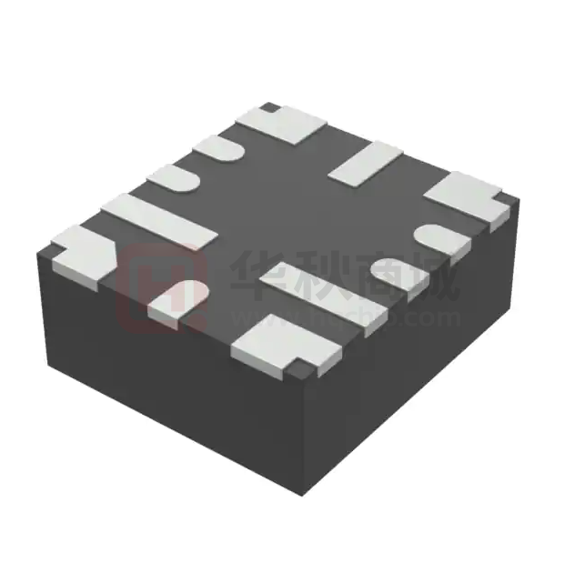


 工商网监
湘ICP备2023018690号
工商网监
湘ICP备2023018690号